US6204159B1 - Method of forming select gate to improve reliability and performance for NAND type flash memory devices - Google Patents
Method of forming select gate to improve reliability and performance for NAND type flash memory devices Download PDFInfo
- Publication number
- US6204159B1 US6204159B1 US09/349,603 US34960399A US6204159B1 US 6204159 B1 US6204159 B1 US 6204159B1 US 34960399 A US34960399 A US 34960399A US 6204159 B1 US6204159 B1 US 6204159B1
- Authority
- US
- United States
- Prior art keywords
- area
- oxide layer
- voltage transistor
- amorphous silicon
- select gate
- Prior art date
- Legal status (The legal status is an assumption and is not a legal conclusion. Google has not performed a legal analysis and makes no representation as to the accuracy of the status listed.)
- Expired - Lifetime
Links
- 238000000034 method Methods 0.000 title claims abstract description 61
- 229910021417 amorphous silicon Inorganic materials 0.000 claims abstract description 74
- 239000000758 substrate Substances 0.000 claims abstract description 50
- 238000000151 deposition Methods 0.000 claims abstract description 28
- OAICVXFJPJFONN-UHFFFAOYSA-N Phosphorus Chemical compound [P] OAICVXFJPJFONN-UHFFFAOYSA-N 0.000 claims description 15
- 229910052698 phosphorus Inorganic materials 0.000 claims description 15
- 239000011574 phosphorus Substances 0.000 claims description 15
- XUIMIQQOPSSXEZ-UHFFFAOYSA-N Silicon Chemical compound [Si] XUIMIQQOPSSXEZ-UHFFFAOYSA-N 0.000 claims description 14
- 229910052710 silicon Inorganic materials 0.000 claims description 14
- 239000010703 silicon Substances 0.000 claims description 14
- WQJQOUPTWCFRMM-UHFFFAOYSA-N tungsten disilicide Chemical compound [Si]#[W]#[Si] WQJQOUPTWCFRMM-UHFFFAOYSA-N 0.000 claims description 12
- 229910021342 tungsten silicide Inorganic materials 0.000 claims description 12
- 150000004767 nitrides Chemical class 0.000 claims description 10
- 229910003818 SiH2Cl2 Inorganic materials 0.000 claims description 3
- 238000011065 in-situ storage Methods 0.000 claims description 3
- 239000000203 mixture Substances 0.000 claims description 3
- 238000004519 manufacturing process Methods 0.000 description 16
- 230000008569 process Effects 0.000 description 15
- 230000003647 oxidation Effects 0.000 description 7
- 238000007254 oxidation reaction Methods 0.000 description 7
- 238000012545 processing Methods 0.000 description 6
- 238000009279 wet oxidation reaction Methods 0.000 description 5
- IJGRMHOSHXDMSA-UHFFFAOYSA-N Atomic nitrogen Chemical compound N#N IJGRMHOSHXDMSA-UHFFFAOYSA-N 0.000 description 4
- QVGXLLKOCUKJST-UHFFFAOYSA-N atomic oxygen Chemical compound [O] QVGXLLKOCUKJST-UHFFFAOYSA-N 0.000 description 4
- 238000005229 chemical vapour deposition Methods 0.000 description 4
- 230000008021 deposition Effects 0.000 description 4
- 238000010586 diagram Methods 0.000 description 4
- 238000005530 etching Methods 0.000 description 4
- 230000006870 function Effects 0.000 description 4
- 239000001301 oxygen Substances 0.000 description 4
- 229910052760 oxygen Inorganic materials 0.000 description 4
- 229920002120 photoresistant polymer Polymers 0.000 description 4
- BLRPTPMANUNPDV-UHFFFAOYSA-N Silane Chemical compound [SiH4] BLRPTPMANUNPDV-UHFFFAOYSA-N 0.000 description 3
- 230000007547 defect Effects 0.000 description 3
- 230000002093 peripheral effect Effects 0.000 description 3
- 229910021420 polycrystalline silicon Inorganic materials 0.000 description 3
- 229920005591 polysilicon Polymers 0.000 description 3
- 239000004065 semiconductor Substances 0.000 description 3
- XKRFYHLGVUSROY-UHFFFAOYSA-N Argon Chemical compound [Ar] XKRFYHLGVUSROY-UHFFFAOYSA-N 0.000 description 2
- BOTDANWDWHJENH-UHFFFAOYSA-N Tetraethyl orthosilicate Chemical compound CCO[Si](OCC)(OCC)OCC BOTDANWDWHJENH-UHFFFAOYSA-N 0.000 description 2
- 238000000137 annealing Methods 0.000 description 2
- 239000005380 borophosphosilicate glass Substances 0.000 description 2
- 230000015556 catabolic process Effects 0.000 description 2
- 238000004140 cleaning Methods 0.000 description 2
- 238000006731 degradation reaction Methods 0.000 description 2
- 238000011161 development Methods 0.000 description 2
- 238000011156 evaluation Methods 0.000 description 2
- 239000007789 gas Substances 0.000 description 2
- 239000001307 helium Substances 0.000 description 2
- 229910052734 helium Inorganic materials 0.000 description 2
- SWQJXJOGLNCZEY-UHFFFAOYSA-N helium atom Chemical compound [He] SWQJXJOGLNCZEY-UHFFFAOYSA-N 0.000 description 2
- 239000001257 hydrogen Substances 0.000 description 2
- 229910052739 hydrogen Inorganic materials 0.000 description 2
- 125000004435 hydrogen atom Chemical class [H]* 0.000 description 2
- 238000007689 inspection Methods 0.000 description 2
- 238000004518 low pressure chemical vapour deposition Methods 0.000 description 2
- 239000000463 material Substances 0.000 description 2
- 229910052757 nitrogen Inorganic materials 0.000 description 2
- 239000005360 phosphosilicate glass Substances 0.000 description 2
- 238000005240 physical vapour deposition Methods 0.000 description 2
- 206010010144 Completed suicide Diseases 0.000 description 1
- 230000004075 alteration Effects 0.000 description 1
- 229910052786 argon Inorganic materials 0.000 description 1
- 238000000429 assembly Methods 0.000 description 1
- 230000000712 assembly Effects 0.000 description 1
- 230000004888 barrier function Effects 0.000 description 1
- 230000015572 biosynthetic process Effects 0.000 description 1
- 230000003292 diminished effect Effects 0.000 description 1
- 230000009977 dual effect Effects 0.000 description 1
- 230000000694 effects Effects 0.000 description 1
- 230000005684 electric field Effects 0.000 description 1
- 239000011261 inert gas Substances 0.000 description 1
- 239000012212 insulator Substances 0.000 description 1
- 229910052751 metal Inorganic materials 0.000 description 1
- 239000002184 metal Substances 0.000 description 1
- 238000012986 modification Methods 0.000 description 1
- 230000004048 modification Effects 0.000 description 1
- 239000012299 nitrogen atmosphere Substances 0.000 description 1
- SBEQWOXEGHQIMW-UHFFFAOYSA-N silicon Chemical compound [Si].[Si] SBEQWOXEGHQIMW-UHFFFAOYSA-N 0.000 description 1
- WFKWXMTUELFFGS-UHFFFAOYSA-N tungsten Chemical compound [W] WFKWXMTUELFFGS-UHFFFAOYSA-N 0.000 description 1
- 229910052721 tungsten Inorganic materials 0.000 description 1
- 239000010937 tungsten Substances 0.000 description 1
- 230000005641 tunneling Effects 0.000 description 1
- 238000001039 wet etching Methods 0.000 description 1
Images


Classifications
-
- H—ELECTRICITY
- H10—SEMICONDUCTOR DEVICES; ELECTRIC SOLID-STATE DEVICES NOT OTHERWISE PROVIDED FOR
- H10B—ELECTRONIC MEMORY DEVICES
- H10B41/00—Electrically erasable-and-programmable ROM [EEPROM] devices comprising floating gates
- H10B41/40—Electrically erasable-and-programmable ROM [EEPROM] devices comprising floating gates characterised by the peripheral circuit region
- H10B41/41—Electrically erasable-and-programmable ROM [EEPROM] devices comprising floating gates characterised by the peripheral circuit region of a memory region comprising a cell select transistor, e.g. NAND
-
- H—ELECTRICITY
- H10—SEMICONDUCTOR DEVICES; ELECTRIC SOLID-STATE DEVICES NOT OTHERWISE PROVIDED FOR
- H10B—ELECTRONIC MEMORY DEVICES
- H10B41/00—Electrically erasable-and-programmable ROM [EEPROM] devices comprising floating gates
- H10B41/40—Electrically erasable-and-programmable ROM [EEPROM] devices comprising floating gates characterised by the peripheral circuit region
- H10B41/42—Simultaneous manufacture of periphery and memory cells
- H10B41/49—Simultaneous manufacture of periphery and memory cells comprising different types of peripheral transistor
-
- H—ELECTRICITY
- H10—SEMICONDUCTOR DEVICES; ELECTRIC SOLID-STATE DEVICES NOT OTHERWISE PROVIDED FOR
- H10B—ELECTRONIC MEMORY DEVICES
- H10B69/00—Erasable-and-programmable ROM [EPROM] devices not provided for in groups H10B41/00 - H10B63/00, e.g. ultraviolet erasable-and-programmable ROM [UVEPROM] devices
Definitions
- the present invention generally relates to simplified methods of making flash memory devices such as EEPROMs. More particularly, the present invention relates to simplified methods of making NAND type flash memory devices characterized by improved select gate performance.
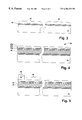
- a memory device such as a flash memory 10 comprises one or more high density core regions 11 and a low density peripheral portion 12 on a single substrate 13 .
- the high density core regions 11 typically consist of at least one M ⁇ N array of individually addressable, substantially identical floating-gate type memory cells and the low density peripheral portion 12 typically includes input/output (I/O) circuitry and circuitry for selectively addressing the individual cells (such as decoders for connecting the source, gate and drain of selected cells to predetermined voltages or impedances to effect designated operations of the cell such as programming, reading or erasing).
- I/O input/output
- Each memory cell 14 has a drain 14 a, a source 14 b and a stacked gate 14 c.
- a plurality of memory cells 14 connected together in series with a drain select transistor at one end and a source select transistor at the other end to form a NAND string as illustrated in prior art FIG. 1 b.
- Each stacked gate 14 c is coupled to a word line (WL 0 , WL 1 , . . . , WLn) while each drain of the drain select transistors are coupled to a bit line (BL 0 , BL 1 , . . . , BLn).
- each source of the source select transistors are coupled to a common source line Vss.
- each memory cell 14 can be addressed for programming, reading or erasing functions.
- FIG. 1 c represents a fragmentary cross section diagram of a typical memory cell 14 in the core region 11 of prior art FIGS. 1 a and 1 b.
- a cell 14 typically includes the source 14 b, the drain 14 a and a channel 15 in a substrate or P-well 16 ; and the stacked gate structure 14 c overlying the channel 15 .
- the stacked gate 14 c further includes a thin gate dielectric layer 17 a (commonly referred to as the tunnel oxide) formed on the surface of the P-well 16 .
- the stacked gate 14 c also includes a polysilicon floating gate 17 b which overlies the tunnel oxide 17 a and an interpoly dielectric layer 17 c overlies the floating gate 17 b.
- the interpoly dielectric layer 17 c is often a multilayer insulator such as an oxide-nitride-oxide (ONO) layer having two oxide layers sandwiching a nitride layer.
- a polysilicon control gate 17 d overlies the interpoly dielectric layer 17 c.
- the control gates 17 d of the respective cells 14 that are formed in a lateral row share a common word line (WL) associated with the row of cells (see, for example, prior art FIG. 1 b ).
- WL word line
- the drain regions 14 a of the respective cells in a vertical column are connected together by a conductive bit line (BL).
- the channel 15 of the cell 14 conducts current between the source 14 b and the drain 14 a in accordance with an electric field developed in the channel 15 by the stacked gate structure 14 c.
- the process for making such NAND type flash memory devices includes numerous individual processing steps. Each flash memory device must be fabricated in the same manner as other flash memory devices to provide consistent performance and reliability. Generally speaking, the fewer the number of processing steps, the easier it is to fabricate uniform flash memory devices.
- fabricating the select gate transistors and the flash memory cells in the core region of NAND type flash memory devices is complicated and involves numerous processing steps.
- Conventional fabrication techniques involve initially growing a select gate oxide over the entire core region or substrate, providing a tunnel oxide mask over the select gate areas, etching the exposed oxide, removing the tunnel oxide mask, cleaning the substrate, and growing a tunnel oxide layer.
- the process may further involve various inspection and evaluation steps after one or more of the numerous processing steps.
- non-volatile flash memory device fabrication is not only simplified, but devices having improved reliability are obtainable.
- simplified methods of the present invention which eliminate the use of steps associated with using a tunnel oxide mask, forming a flash memory device having a low defect density, minimized charge gain/loss concerns from high/low Poly 1 doping, and fewer select gate interconnection problems is facilitated.
- the present invention relates to a method of forming a NAND type flash memory device, involving the steps of growing a first oxide layer over at least a portion of a substrate, the substrate including a core region and a periphery region, the core region including a flash memory cell area and a select gate area and the periphery region including a high voltage transistor area and low voltage transistor area; depositing a first doped amorphous silicon layer over at least a portion of the first oxide layer; depositing a dielectric layer over at least a portion of the first doped amorphous silicon layer; removing portions of the first oxide layer, the first doped amorphous silicon layer, and the dielectric layer in the select gate area of the core region and the high voltage transistor area and the low voltage transistor area the periphery region; growing a second oxide layer over at least a portion of the substrate in the select gate area of the core region and the high voltage transistor area and the low voltage transistor area the periphery region; removing portions of the second oxide layer in the
- the present invention relates to a method of forming a flash memory cell and a select gate of a NAND type flash memory device, involving the steps of growing a first oxide layer having a thickness from about 70 ⁇ to about 110 ⁇ over at least a portion of a substrate, the substrate including a core region, the core region including a flash memory cell area and a select gate area; depositing a first doped amorphous silicon layer over at least a portion of the first oxide layer; depositing a dielectric layer over at least a portion of the first doped amorphous silicon layer; removing portions of the first oxide layer, the first doped amorphous silicon layer, and the dielectric layer in the select gate area of the core region; growing a second oxide layer having a thickness from about 150 ⁇ to about 190 ⁇ over at least a portion of the substrate in the select gate area of the core region; depositing a second doped amorphous silicon layer over at least a portion of the dielectric layer and the second oxide layer; and forming
- the present invention relates to a method of forming a NAND type flash memory device, involving the steps of growing a first oxide layer having a thickness from about 70 ⁇ to about 110 ⁇ over at least a portion of a substrate, the substrate including a core region and a periphery region, the core region including a flash memory cell area and a select gate area and the periphery region including a high voltage transistor area and low voltage transistor area; depositing a first phosphorus doped amorphous silicon layer over at least a portion of the first oxide layer; depositing a multilayer dielectric over at least a portion of the first phosphorus doped amorphous silicon layer; removing portions of the first oxide layer, the first phosphorus doped amorphous silicon layer, and the multilayer dielectric in the select gate area of the core region and the high voltage transistor area and the low voltage transistor area the periphery region; growing a second oxide layer having a thickness from about 260 ⁇ to about 300 ⁇ over at least a portion
- FIG. 1 a is a plan view illustrating a prior art layout of a flash memory chip
- FIG. 1 b is a schematic diagram illustrating a prior art NAND-type flash memory circuit configuration
- FIG. 1 c is a fragmentary cross section illustrating a prior art stacked gate flash memory cell.
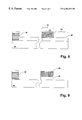
- FIG. 2 a is a schematic diagram illustrating a core portion of a NAND-type flash memory device.
- FIG. 2 b is a plan layout view of the core portion of the NAND-type flash memory device of FIG. 2 a.
- FIG. 3 is a cross sectional illustration of one aspect of a method of making a NAND type flash memory device in accordance with the present invention.
- FIG. 4 is a cross sectional illustration of one aspect of a method of making a NAND type flash memory device in accordance with the present invention.
- FIG. 5 is a cross sectional illustration of one aspect of a method of making a NAND type flash memory device in accordance with the present invention.
- FIG. 6 is a cross sectional illustration of one aspect of a method of making a NAND type flash memory device in accordance with the present invention.
- FIG. 7 is a cross sectional illustration of one aspect of a method of making a NAND type flash memory device in accordance with the present invention.
- FIG. 8 is a cross sectional illustration of one aspect of a method of making a NAND type flash memory device in accordance with the present invention.
- FIG. 9 is a cross sectional illustration of one aspect of a method of making a NAND type flash memory device in accordance with the present invention.
- FIG. 10 is a cross sectional illustration of one aspect of a method of making a NAND type flash memory device in accordance with the present invention.
- FIG. 11 is a cross sectional illustration of one aspect of a method of making a NAND type flash memory device in accordance with the present invention.
- FIG. 12 is a cross sectional illustration of a NAND type flash memory device in accordance with the present invention.
- FIG. 13 is another cross sectional illustration of a NAND type flash memory device in accordance with the present invention.
- non-volatile flash memory device fabrication is not only simplified, but devices having improved reliability are obtainable.
- simplified methods of the present invention which eliminate the use of steps associated with using a tunnel oxide mask, forming a flash memory device having a low defect density, minimized charge gain/loss concerns from high/low Poly 1 doping, and fewer select gate interconnection problems is facilitated.
- the present invention relates to a flash memory device and a method for its manufacture that, according to one aspect of the present invention, eliminates the dual core oxide processing steps. Consequently, the steps used in forming the high and low voltage gate transistor structures of the periphery region may be used to construct the select gate transistors, thereby substantially reducing the number of processing steps needed to construct the flash memory device.
- FIG. 2 a A circuit schematic diagram illustrating a core portion 11 of a NAND-type flash memory device is illustrated in FIG. 2 a.
- the core portion 11 includes a memory cell region 22 which is bounded on one side by a drain select transistor portion 24 and bounded on another side by a source select transistor portion 26 .
- Each of the select transistor portions 24 and 26 contain select gate transistors 24 a - 24 c and 26 a - 26 c, respectively, which operate to selectively activate a desired bit line (for example, BLN ⁇ 1, BLN, BLN+1) by ensuring the selectivity of each bit line and preventing the cell current from conducting current through the bit line during a programming operation as is known by those skilled in the art.
- a desired bit line for example, BLN ⁇ 1, BLN, BLN+1
- a simplified tunnel and gate oxide process is used to form the memory cell oxides and the select gate transistor oxides, respectively (since the memory cell oxides and select gate transistor oxides have different thicknesses).
- formation of the high and low voltage transistors in the periphery region 14 and in particular their corresponding oxides are incorporated into the processes (see, for example, FIG. 1 ).
- the process may further include a double doped amorphous silicon layer to generate stacked gate structures in the core region 12 .
- the core select gate transistors 24 a - 24 c and 26 a - 26 c are somewhat similar in structure to the stacked gate flash memory structures in the memory cell region 22 except that their gate oxide is approximately twice as thick as the cell oxide (also called the tunnel oxide) in the stacked gate structure of the memory cell (about 170 ⁇ compared to about 90 ⁇ ).
- the select transistors 24 a - 24 c utilize a gate oxide of about 170 ⁇ to improve the reliability of the transistors by reducing the vulnerability of the devices to band to band tunneling induced hot carrier stress during programming.
- the select gate transistors 24 a - 24 c and 26 a - 26 c further differ from the stacked gate flash memory cell structures of the region 22 because they operate as conventional MOS transistors and therefore have one doped amorphous silicon layer as a standard MOS transistor configuration.
- a plan circuit layout view of the conventional NAND-type circuit arrangement 12 is illustrated in FIG. 2 b.
- a first gate oxide is grown using any suitable means, such as dry oxidation, wet oxidation or thermal oxidation, on at least a portion of a semiconductor substrate (the core and periphery regions) typically made of silicon.
- the first gate oxide later serves as the stacked memory cell tunnel oxide.
- the first gate oxide or stacked memory cell tunnel oxide has a thickness from about 70 ⁇ to about 110 ⁇ . In another embodiment, the stacked memory cell tunnel oxide has a thickness from about 80 ⁇ to about 110 ⁇ .
- a first doped amorphous silicon layer is provided using any suitable means over at least a portion of the first gate oxide (over the core and periphery regions).
- the first doped amorphous silicon layer later serves as the floating gate of the stacked memory cell (also termed Poly 1).
- the first doped amorphous silicon layer has a thickness from about 700 ⁇ to about 1,100 ⁇ , and preferably from about 800 ⁇ to about 1,000 ⁇ .
- a dielectric layer is provided using any suitable means over at least a portion of the first doped amorphous silicon layer.
- the dielectric layer preferably contains three layers; namely two oxide layers sandwiching a nitride layer (a so-called ONO layer).
- the dielectric layer later serves as the interpoly dielectric layer of the stacked memory cell.
- the dielectric layer has a thickness from about 100 ⁇ to about 160 ⁇ , and preferably from about 120 ⁇ to about 140 ⁇ .
- a mask such as a suitable photoresist is used to cover the stacked memory cell areas of the core region and the exposed portion of the substrate is etched down to the silicon substrate (the dielectric layer, the first doped amorphous silicon layer and first gate oxide are removed in the periphery region and select gate areas of the core region). Multiple etching steps may be employed to remove the dielectric layer, the first doped amorphous silicon layer and first gate oxide.
- a second gate oxide layer is provided using any suitable means, such as dry oxidation, wet oxidation or thermal oxidation, on at least a portion of the exposed portions of the silicon substrate (over a portion of the core region and over all of the periphery region).
- the second gate oxide later serves as the gate oxide for subsequently formed high voltage transistors in the periphery region.
- the second gate oxide has a thickness from about 260 ⁇ to about 300 ⁇ .
- the second gate oxide has a thickness from about 270 ⁇ to about 290 ⁇ .
- the second gate oxide layer has a thickness that is greater than the first gate oxide layer (the second gate oxide layer also has a thickness that is greater than the third gate oxide layer discussed below).
- a mask such as a suitable photoresist is used to cover the high voltage transistor areas of the periphery region and the exposed portions of the second gate oxide layer are etched down to the silicon substrate (the second gate oxide in the low voltage transistor area of the periphery region and the select gate areas of the core region is removed) using suitable etch techniques such as wet etch techniques.
- the mask may, if necessary, cover the stacked memory cell areas of the core region to prevent degradation of the dielectric layer.
- a third gate oxide layer is provided using any suitable means, such as dry oxidation, wet oxidation or thermal oxidation, over at least a portion of the exposed portions of the silicon substrate (over the low voltage transistor area of the periphery region and the select gate areas of the core region).
- the third gate oxide later serves as the gate oxide for subsequently formed low voltage transistors in the periphery region and the select gate transistors in the core region.
- the third gate oxide has a thickness from about 150 ⁇ to about 190 ⁇ .
- the third gate oxide has a thickness from about 160 ⁇ to about 180 ⁇ .
- the third gate oxide layer has a thickness that is greater than the first gate oxide layer.
- a second doped amorphous silicon layer is provided using any suitable means over at least a portion of the substrate (over the core and periphery regions).
- the second doped amorphous silicon layer later serves as the control gate of the stacked memory cell (also termed Poly 2), the select gate, the high voltage gate and the low voltage gate.
- the second doped amorphous silicon layer has a thickness from about 1,000 ⁇ to about 1,400 ⁇ , and preferably from about 1,100 ⁇ to about 1,300 ⁇ .
- Additional layers are provided using any suitable means over portions of the second doped amorphous silicon layer. For example, a tungsten silicide layer and a silicon oxynitride layer may be provided over the second doped amorphous silicon layer.
- a series of masks and etch steps are employed to form various structures including flash memory cells, select gates, low voltage gates, high voltage gates, word lines, interconnections, and the like.
- the Poly 2 is used as a conductive layer instead of Poly 1 as in conventional configurations.
- This aspect of the present invention not only simplifies the fabrication process, but also improves the quality and reliability of the resultant flash memory devices produced thereby. That is, contact performance using a Poly 2 contact is generally more reliable and better performing than a Poly 1 contact.
- Steps associated with the use of a tunnel oxide mask may be eliminated according to the present invention. These steps include an initial growth of an oxide having a thickness approximately appropriate for a select gate but too thick for a tunnel oxide, tunnel oxide mask and etching steps, and cleaning, inspection and evaluation steps.
- the first doped amorphous silicon layer (Poly 1) is used as the floating gate region for the core memory cells and the second doped amorphous silicon silicon layer (Poly 2) is used for the core memory cell control gates, the select gates in the core region and the gate regions for the periphery transistors (both high and low voltage).
- the NAND-type process involves the fabrication of at least two types of devices including four types of devices; namely a stacked gate memory cell in the core region, a select gate transistor in the core region, a periphery low voltage transistor and a periphery high voltage transistor.
- the substrate 30 is typically a silicon substrate optionally with various elements, regions and/or layers thereover; including metal layers, barrier layers, dielectric layers, device structures, active regions such as active silicon regions or areas, active elements and passive elements including P wells, N wells, additional polysilicon gates, wordlines, source regions, drain regions, bit lines, bases, emitters, collectors, conductive lines, conductive plugs, etc.
- the substrate 30 has two main regions; namely, a core region 32 and a periphery region 34 .
- a first gate oxide 36 is provided over at least a portion of the substrate 30 or over the entire substrate 30 .
- the first gate oxide 36 which subsequently forms a memory cell tunnel oxide (see FIG. 12) has a thickness of about 87 ⁇ in this embodiment.
- the first gate oxide 36 in this embodiment is formed by a dry oxidation process at about 1050° C. under 1.33 l of oxygen, 70 cc HCl, and 12.6 l of argon.
- a first doped amorphous silicon layer 38 is provided using an in situ doping process over at least a portion of the first gate oxide 36 .
- a phosphorus doped amorphous silicon layer is deposited via chemical vapor deposition (CVD) to form a doped amorphous silicon layer 38 at 530° C., 400 mTorr, SiH 4 at 2000 sccm, and a mixture of 1% by weight PH 3 in helium at about 22 sccm.
- the first doped amorphous silicon layer 38 also termed Poly 1) subsequently forms the floating gate (see FIG. 12) of the stacked memory cell.
- the first doped amorphous silicon layer 38 has a thickness of about 900 ⁇ .
- a dielectric layer 40 is provided over at least a portion of the first doped amorphous silicon layer 38 .
- the dielectric layer 40 is an ONO multilayer dielectric containing three layers; namely an oxide layer 40 a, a nitride layer 40 b, and another oxide layer 40 c.
- the dielectric layer subsequently forms the interpoly dielectric layer (see FIG. 12) of the stacked memory cell.
- the dielectric layer has a thickness of about 130 ⁇ .
- Oxide layer 40 a is deposited at a temperature of about 750° C. under SiH 4 at 20 cc, N 2 O at 1.2 l and a pressure of 600 mTorr via low pressure CVD (LPCVD) on the first doped amorphous silicon layer 38 .
- LPCVD low pressure CVD
- Nitride is next deposited at a temperature of about 760° C. under NH 3 at 600 cc, SiH 2 Cl 2 at 100 cc and a pressure of 330 mTorr to form a nitride layer 40 b.
- the nitride layer 40 b is oxidized with wet oxygen at a temperature of about 950° C. under O 2 at 5 l and H 2 at 9 l for 40 minutes to form another oxide layer 40 c.
- a mask 42 is used to cover the stacked memory cell areas 46 of the core region 32 leaving the dielectric layer 40 exposed in the select gate area 44 of the core region 32 and in the periphery region 34 .
- the core region 32 contains select gate areas 44 and stacked memory cell areas 46 .
- the mask 42 contains a suitable photoresist material and is formed using suitable photolithographic techniques including spin on deposition, selective irradiation, and development.
- the exposed portion of the structure is etched down to the substrate 30 .
- portions of the dielectric layer 40 , the first doped amorphous silicon layer 38 and first gate oxide 36 are removed in the periphery region 34 and select gate areas 44 of the core region 32 using suitable etching techniques, including wet etching techniques.
- second gate oxide layer 48 is provided on at least a portion of the exposed portions of the substrate 30 (over the select gate area 44 of the core region 32 and over the periphery region 34 ).
- the second gate oxide layer 48 is formed by wet oxidation at about 800° C. under 6.4 l oxygen, 2.133 l of hydrogen, and 75 cc of HCl, and optionally annealing at about 900° C. under nitrogen.
- the second gate oxide 48 subsequently forms the gate oxide for the high voltage transistors in the periphery region (see FIG. 12 ).
- the second gate oxide layer 48 has a thickness of about 285 ⁇ .
- a mask 50 is positioned to cover the high voltage transistor areas 52 of the periphery region 34 .
- the periphery region 34 contains high voltage transistor areas 52 and low voltage transistor areas 54 .
- the mask 50 contains a suitable photoresist material and is formed using suitable photolithographic techniques including spin on deposition, selective irradiation, and development. Although not shown, the mask 50 may also cover the stacked memory cell areas 46 of the core region 32 to prevent degradation of the dielectric layer 40 .
- the exposed portions of the second gate oxide layer 48 are etched down to the silicon substrate (the second gate oxide in the low voltage transistor area 54 of the periphery region 34 and the select gate areas 44 of the core region 32 is removed). Any suitable oxide selective etchant may be employed.
- a third gate oxide layer 56 and 58 is provided on at least a portion of the exposed portions of the substrate 30 (over the select gate area 44 of the core region 32 ( 56 ) and over the low voltage transistor area 54 the periphery region 34 ( 58 )).
- the third gate oxide layer 56 and 58 is formed by wet oxidation at about 800° C. under 6.4 l oxygen, 2.133 l of hydrogen, and 75 cc of HCl, and optionally annealing at about 900° C. under nitrogen.
- the third gate oxide layer 56 and 58 subsequently forms the gate oxides for the select gate transistors in the core region and the low voltage transistors in the periphery region (see FIG. 12 ).
- the third gate oxide layer 56 and 58 has a thickness of about 168 ⁇ .
- a second doped amorphous silicon layer 60 is provided over at least a portion of the substrate (over the core region 32 and periphery region 34 ).
- the phosphorus doped amorphous silicon layer is deposited via CVD to form a doped amorphous silicon layer 60 at 530° C., 400 mTorr, SiH 4 at 2000 sccm, and a mixture of 1% by weight PH 3 in helium at about 22 sccm.
- the second doped amorphous silicon layer 60 has a thickness of about 1,200 ⁇ .
- the second doped amorphous silicon layer 60 subsequently forms the control gate of the stacked memory cell (also termed Poly 2), the select gate, the high voltage gate and the low voltage gate (see FIG. 12 ).
- a tungsten silicide layer 62 is provided over at least a portion of the second doped amorphous silicon layer 60 .
- the tungsten silicide layer 62 may be formed by suitable means.
- the tungsten silicide is deposited via CVD techniques at a temperature of about 565° C. and a pressure of about 93 Pa.
- the gas flow includes SiH 2 Cl 2 and WF 6 .
- the gas flow may further contain an inert gas, such as Ar.
- RTA rapid thermal anneal
- the tungsten silicide layer 62 has a thickness from about 1,000 ⁇ to about 1,800 ⁇ , but in this embodiment, the thickness is about 1,400 ⁇ .
- a silicon oxynitride layer 64 is provided over at least a portion of the tungsten silicide layer 62 .
- the silicon oxynitride layer 64 is formed via suitable techniques including via physical vapor deposition (PVD) techniques. Methods of forming silicon oxynitride are known in the art.
- the silicon oxynitride layer 64 has a thickness from about 800 ⁇ to about 1,200 ⁇ , but in this embodiment, the thickness is about 1,000 ⁇ .
- a series of masks and etch steps are employed to form various structures including a stacked flash memory cell 66 , a select gate transistor 68 , a high voltage gate transistor 70 , and a low voltage gate transistor 72 .
- various contacts and interconnects may be formed, as well as the deposition of an encapsulating oxide film, such as tetraethylorthosilicate (TEOS), borophosphotetraethylorthosilicate (BPTEOS), phosphosilicate glass (PSG), or borophosphosilicate glass (BPSG).
- TEOS tetraethylorthosilicate
- BPTEOS borophosphotetraethylorthosilicate
- PSG phosphosilicate glass
- BPSG borophosphosilicate glass
- FIG. 13 an illustration of a flash memory device made in accordance with the present invention is shown along a word line.
- substrate 30 On substrate 30 , are field oxide regions 74 (not shown in FIG. 3 - 12 ), first gate oxide 36 (tunnel oxide), a first doped amorphous silicon layer 38 (Poly 1), dielectric layer 40 (such as an ONO multilayer dielectric), and a second doped amorphous silicon layer 60 (Poly 2).
Abstract
Description
Claims (20)
Priority Applications (6)
| Application Number | Priority Date | Filing Date | Title |
|---|---|---|---|
| US09/349,603 US6204159B1 (en) | 1999-07-09 | 1999-07-09 | Method of forming select gate to improve reliability and performance for NAND type flash memory devices |
| JP2001509080A JP2003504872A (en) | 1999-07-09 | 2000-06-29 | New method of forming select gates to improve reliability and performance for NAND flash memory devices |
| PCT/US2000/017912 WO2001004948A1 (en) | 1999-07-09 | 2000-06-29 | New method of forming select gate to improve reliability and performance for nand type flash memory devices |
| EP00943282A EP1198834A1 (en) | 1999-07-09 | 2000-06-29 | New method of forming select gate to improve reliability and performance for nand type flash memory devices |
| KR1020027000333A KR100724153B1 (en) | 1999-07-09 | 2000-06-29 | New method of forming select gate to improve reliability and performance for nand type flash memory devices |
| TW089113511A TW530414B (en) | 1999-07-09 | 2000-07-07 | Method of forming select gate to improve reliability and performance for NAND type flash memory devices |
Applications Claiming Priority (1)
| Application Number | Priority Date | Filing Date | Title |
|---|---|---|---|
| US09/349,603 US6204159B1 (en) | 1999-07-09 | 1999-07-09 | Method of forming select gate to improve reliability and performance for NAND type flash memory devices |
Publications (1)
| Publication Number | Publication Date |
|---|---|
| US6204159B1 true US6204159B1 (en) | 2001-03-20 |
Family
ID=23373162
Family Applications (1)
| Application Number | Title | Priority Date | Filing Date |
|---|---|---|---|
| US09/349,603 Expired - Lifetime US6204159B1 (en) | 1999-07-09 | 1999-07-09 | Method of forming select gate to improve reliability and performance for NAND type flash memory devices |
Country Status (6)
| Country | Link |
|---|---|
| US (1) | US6204159B1 (en) |
| EP (1) | EP1198834A1 (en) |
| JP (1) | JP2003504872A (en) |
| KR (1) | KR100724153B1 (en) |
| TW (1) | TW530414B (en) |
| WO (1) | WO2001004948A1 (en) |
Cited By (14)
| Publication number | Priority date | Publication date | Assignee | Title |
|---|---|---|---|---|
| US6329249B1 (en) * | 1998-06-15 | 2001-12-11 | Samsung Electronics Co., Ltd. | Method for fabricating a semiconductor device having different gate oxide layers |
| US20020127799A1 (en) * | 2001-03-12 | 2002-09-12 | Hyeon-Seag Kim | High voltage oxidation method for highly reliable flash memory devices |
| US20030030097A1 (en) * | 2001-08-09 | 2003-02-13 | Samsung Electronics Co., Ltd. | Non-volatile memory device having floating trap type memory cell and method of forming the same |
| US6611019B2 (en) * | 1999-09-01 | 2003-08-26 | Micron Technology, Inc. | Method and structure for an improved floating gate memory cell |
| US6673520B2 (en) * | 2001-08-24 | 2004-01-06 | Motorola, Inc. | Method of making an integrated circuit using a reflective mask |
| US6720133B1 (en) * | 2002-04-19 | 2004-04-13 | Advanced Micro Devices, Inc. | Memory manufacturing process using disposable ARC for wordline formation |
| US20040203204A1 (en) * | 2002-01-09 | 2004-10-14 | Chun-Lein Su | Fabrication method for a flash memory device |
| US7141480B2 (en) * | 2004-03-26 | 2006-11-28 | Texas Instruments Incorporated | Tri-gate low power device and method for manufacturing the same |
| US7179709B2 (en) | 2004-08-13 | 2007-02-20 | Samsung Electronics, Co., Ltd. | Method of fabricating non-volatile memory device having local SONOS gate structure |
| US20080248622A1 (en) * | 2007-04-02 | 2008-10-09 | George Matamis | Methods Of Fabricating Non-Volatile Memory With Integrated Peripheral Circuitry And Pre-Isolation Memory Cell Formation |
| US20080248621A1 (en) * | 2007-04-02 | 2008-10-09 | James Kai | Integrated Non-Volatile Memory And Peripheral Circuitry Fabrication |
| US20080268630A1 (en) * | 2007-04-30 | 2008-10-30 | Spansion Llc | Method to obtain multiple gate thicknesses using in-situ gate etch mask approach |
| US20080268650A1 (en) * | 2007-04-30 | 2008-10-30 | Spansion Llc | Triple poly-si replacement scheme for memory devices |
| WO2017065938A1 (en) * | 2015-10-12 | 2017-04-20 | Silicon Storage Technology, Inc. | Method of forming memory array and logic devices |
Families Citing this family (6)
| Publication number | Priority date | Publication date | Assignee | Title |
|---|---|---|---|---|
| KR100389039B1 (en) * | 2001-03-05 | 2003-06-25 | 삼성전자주식회사 | Non-volatile memory device and fabrication method thereof |
| KR100854896B1 (en) * | 2002-06-05 | 2008-08-28 | 주식회사 하이닉스반도체 | Method for manufacturing flash memory device |
| KR100647482B1 (en) * | 2004-09-16 | 2006-11-23 | 삼성전자주식회사 | Semiconductor Device and Method of Manufacturing the same |
| JP2007180482A (en) | 2005-12-28 | 2007-07-12 | Hynix Semiconductor Inc | Manufacturing method for flash memory element |
| US8464137B2 (en) | 2010-12-03 | 2013-06-11 | International Business Machines Corporation | Probabilistic multi-tier error correction in not-and (NAND) flash memory |
| US9123579B2 (en) * | 2013-03-13 | 2015-09-01 | Macronix International Co., Ltd. | 3D memory process and structures |
Citations (13)
| Publication number | Priority date | Publication date | Assignee | Title |
|---|---|---|---|---|
| US5008212A (en) * | 1988-12-12 | 1991-04-16 | Chen Teh Yi J | Selective asperity definition technique suitable for use in fabricating floating-gate transistor |
| US5278439A (en) | 1991-08-29 | 1994-01-11 | Ma Yueh Y | Self-aligned dual-bit split gate (DSG) flash EEPROM cell |
| US5427967A (en) * | 1993-03-11 | 1995-06-27 | National Semiconductor Corporation | Technique for making memory cells in a way which suppresses electrically conductive stringers |
| US5429969A (en) * | 1994-05-31 | 1995-07-04 | Motorola, Inc. | Process for forming electrically programmable read-only memory cell with a merged select/control gate |
| US5445983A (en) | 1994-10-11 | 1995-08-29 | United Microelectronics Corporation | Method of manufacturing EEPROM memory device with a select gate |
| US5498559A (en) * | 1994-06-20 | 1996-03-12 | Motorola, Inc. | Method of making a nonvolatile memory device with five transistors |
| US5637895A (en) | 1994-09-02 | 1997-06-10 | Kabushiki Kaisha Toshiba | Non-volatile semiconductor memory device |
| US5793079A (en) | 1996-07-22 | 1998-08-11 | Catalyst Semiconductor, Inc. | Single transistor non-volatile electrically alterable semiconductor memory device |
| US5805499A (en) | 1997-02-28 | 1998-09-08 | Advanced Micro Devices, Inc. | Channel hot-carrier page write for NAND applications |
| US5856943A (en) | 1996-03-18 | 1999-01-05 | Integrated Memory Technologies, Inc. | Scalable flash EEPROM memory cell and array |
| US5879990A (en) * | 1996-03-22 | 1999-03-09 | U.S. Philips Corporation | Semiconductor device having an embedded non-volatile memory and method of manufacturing such a semicondutor device |
| US5963806A (en) * | 1996-12-09 | 1999-10-05 | Mosel Vitelic, Inc. | Method of forming memory cell with built-in erasure feature |
| US6040216A (en) * | 1997-08-11 | 2000-03-21 | Mosel Vitelic, Inc. | Method (and device) for producing tunnel silicon oxynitride layer |
Family Cites Families (17)
| Publication number | Priority date | Publication date | Assignee | Title |
|---|---|---|---|---|
| JPS6273774A (en) * | 1985-09-27 | 1987-04-04 | Toshiba Corp | Manufacture of semiconductor memory |
| US4874716A (en) * | 1986-04-01 | 1989-10-17 | Texas Instrument Incorporated | Process for fabricating integrated circuit structure with extremely smooth polysilicone dielectric interface |
| JP2856811B2 (en) * | 1990-01-30 | 1999-02-10 | 株式会社東芝 | Method of manufacturing nonvolatile semiconductor memory device |
| JPH04302476A (en) * | 1991-03-29 | 1992-10-26 | Toshiba Corp | Manufacture of nonvolatile semiconductor memory |
| JPH05283710A (en) * | 1991-12-06 | 1993-10-29 | Intel Corp | High-voltage mos transistor and manufacture thereof |
| JPH05275707A (en) * | 1992-03-30 | 1993-10-22 | Toshiba Corp | Manufacture of nonvolatile semiconductor memory device |
| KR960012303B1 (en) * | 1992-08-18 | 1996-09-18 | 삼성전자 주식회사 | Non-volatile semiconductor memory device and manufacturing thereof |
| JP3600326B2 (en) * | 1994-09-29 | 2004-12-15 | 旺宏電子股▲ふん▼有限公司 | Nonvolatile semiconductor memory device and manufacturing method thereof |
| US5622881A (en) * | 1994-10-06 | 1997-04-22 | International Business Machines Corporation | Packing density for flash memories |
| JPH08306889A (en) * | 1995-05-08 | 1996-11-22 | Toshiba Corp | Non-volatile semiconductor memory device and its fabrication method |
| JPH09260513A (en) * | 1996-03-25 | 1997-10-03 | Fujitsu Ltd | Semiconductor device and its manufacture |
| EP0811983A1 (en) * | 1996-06-06 | 1997-12-10 | STMicroelectronics S.r.l. | Flash memory cell, electronic device comprising such a cell, and relative fabrication method |
| JP3442596B2 (en) * | 1996-11-28 | 2003-09-02 | 富士通株式会社 | Method for manufacturing semiconductor device |
| EP0877416A1 (en) * | 1997-05-08 | 1998-11-11 | STMicroelectronics S.r.l. | Integrated structure comprising a polysilicon element with large grain size |
| US5861347A (en) * | 1997-07-03 | 1999-01-19 | Motorola Inc. | Method for forming a high voltage gate dielectric for use in integrated circuit |
| JP3586072B2 (en) * | 1997-07-10 | 2004-11-10 | 株式会社東芝 | Nonvolatile semiconductor memory device |
| JPH11126834A (en) * | 1997-10-24 | 1999-05-11 | Denso Corp | Semiconductor device and manufacture thereof |
-
1999
- 1999-07-09 US US09/349,603 patent/US6204159B1/en not_active Expired - Lifetime
-
2000
- 2000-06-29 WO PCT/US2000/017912 patent/WO2001004948A1/en active Application Filing
- 2000-06-29 KR KR1020027000333A patent/KR100724153B1/en not_active IP Right Cessation
- 2000-06-29 EP EP00943282A patent/EP1198834A1/en not_active Withdrawn
- 2000-06-29 JP JP2001509080A patent/JP2003504872A/en active Pending
- 2000-07-07 TW TW089113511A patent/TW530414B/en not_active IP Right Cessation
Patent Citations (13)
| Publication number | Priority date | Publication date | Assignee | Title |
|---|---|---|---|---|
| US5008212A (en) * | 1988-12-12 | 1991-04-16 | Chen Teh Yi J | Selective asperity definition technique suitable for use in fabricating floating-gate transistor |
| US5278439A (en) | 1991-08-29 | 1994-01-11 | Ma Yueh Y | Self-aligned dual-bit split gate (DSG) flash EEPROM cell |
| US5427967A (en) * | 1993-03-11 | 1995-06-27 | National Semiconductor Corporation | Technique for making memory cells in a way which suppresses electrically conductive stringers |
| US5429969A (en) * | 1994-05-31 | 1995-07-04 | Motorola, Inc. | Process for forming electrically programmable read-only memory cell with a merged select/control gate |
| US5498559A (en) * | 1994-06-20 | 1996-03-12 | Motorola, Inc. | Method of making a nonvolatile memory device with five transistors |
| US5637895A (en) | 1994-09-02 | 1997-06-10 | Kabushiki Kaisha Toshiba | Non-volatile semiconductor memory device |
| US5445983A (en) | 1994-10-11 | 1995-08-29 | United Microelectronics Corporation | Method of manufacturing EEPROM memory device with a select gate |
| US5856943A (en) | 1996-03-18 | 1999-01-05 | Integrated Memory Technologies, Inc. | Scalable flash EEPROM memory cell and array |
| US5879990A (en) * | 1996-03-22 | 1999-03-09 | U.S. Philips Corporation | Semiconductor device having an embedded non-volatile memory and method of manufacturing such a semicondutor device |
| US5793079A (en) | 1996-07-22 | 1998-08-11 | Catalyst Semiconductor, Inc. | Single transistor non-volatile electrically alterable semiconductor memory device |
| US5963806A (en) * | 1996-12-09 | 1999-10-05 | Mosel Vitelic, Inc. | Method of forming memory cell with built-in erasure feature |
| US5805499A (en) | 1997-02-28 | 1998-09-08 | Advanced Micro Devices, Inc. | Channel hot-carrier page write for NAND applications |
| US6040216A (en) * | 1997-08-11 | 2000-03-21 | Mosel Vitelic, Inc. | Method (and device) for producing tunnel silicon oxynitride layer |
Cited By (37)
| Publication number | Priority date | Publication date | Assignee | Title |
|---|---|---|---|---|
| US6329249B1 (en) * | 1998-06-15 | 2001-12-11 | Samsung Electronics Co., Ltd. | Method for fabricating a semiconductor device having different gate oxide layers |
| US20050009276A1 (en) * | 1999-09-01 | 2005-01-13 | Micron Technology, Inc. | Methods and structure for an improved floating gate memory cell |
| US6611019B2 (en) * | 1999-09-01 | 2003-08-26 | Micron Technology, Inc. | Method and structure for an improved floating gate memory cell |
| US7015098B2 (en) | 1999-09-01 | 2006-03-21 | Micron Technology, Inc. | Methods and structure for an improved floating gate memory cell |
| US6849501B2 (en) | 1999-09-01 | 2005-02-01 | Micron Technology, Inc. | Methods for fabricating an improved floating gate memory cell |
| US20030203557A1 (en) * | 1999-09-01 | 2003-10-30 | Micron Technology, Inc. | Method and structure for an improved floating gate memory cell |
| US6534363B2 (en) * | 2001-03-12 | 2003-03-18 | Advanced Micro Devices, Inc. | High voltage oxidation method for highly reliable flash memory devices |
| US20020127799A1 (en) * | 2001-03-12 | 2002-09-12 | Hyeon-Seag Kim | High voltage oxidation method for highly reliable flash memory devices |
| US20040023451A1 (en) * | 2001-08-09 | 2004-02-05 | Chang-Hyun Lee | Non-volatile memory device having floating trap type memory cell and method of forming the same |
| US20030030097A1 (en) * | 2001-08-09 | 2003-02-13 | Samsung Electronics Co., Ltd. | Non-volatile memory device having floating trap type memory cell and method of forming the same |
| DE10235986B4 (en) * | 2001-08-09 | 2010-11-25 | Samsung Electronics Co., Ltd., Suwon | A non-volatile memory device having a floating trap memory cell and method of making the same |
| US7084030B2 (en) | 2001-08-09 | 2006-08-01 | Samsung Electronics Co., Ltd. | Method of forming a non-volatile memory device having floating trap type memory cell |
| US6781193B2 (en) | 2001-08-09 | 2004-08-24 | Samsung Electronics Co., Ltd. | Non-volatile memory device having floating trap type memory cell and method of forming the same |
| US6673520B2 (en) * | 2001-08-24 | 2004-01-06 | Motorola, Inc. | Method of making an integrated circuit using a reflective mask |
| US6841446B2 (en) * | 2002-01-09 | 2005-01-11 | Macronix International Co., Ltd. | Fabrication method for a flash memory device |
| US20040203204A1 (en) * | 2002-01-09 | 2004-10-14 | Chun-Lein Su | Fabrication method for a flash memory device |
| US6720133B1 (en) * | 2002-04-19 | 2004-04-13 | Advanced Micro Devices, Inc. | Memory manufacturing process using disposable ARC for wordline formation |
| US7141480B2 (en) * | 2004-03-26 | 2006-11-28 | Texas Instruments Incorporated | Tri-gate low power device and method for manufacturing the same |
| US7179709B2 (en) | 2004-08-13 | 2007-02-20 | Samsung Electronics, Co., Ltd. | Method of fabricating non-volatile memory device having local SONOS gate structure |
| US20080248622A1 (en) * | 2007-04-02 | 2008-10-09 | George Matamis | Methods Of Fabricating Non-Volatile Memory With Integrated Peripheral Circuitry And Pre-Isolation Memory Cell Formation |
| WO2008122012A2 (en) * | 2007-04-02 | 2008-10-09 | Sandisk Corporation | Integrated non-volatile memory and peripheral circuitry fabrication |
| US20080268596A1 (en) * | 2007-04-02 | 2008-10-30 | Tuan Pham | Methods Of Fabricating Non-Volatile Memory With Integrated Select And Peripheral Circuitry And Post-Isolation Memory Cell Formation |
| TWI387059B (en) * | 2007-04-02 | 2013-02-21 | Sandisk Technologies Inc | Integrated non-volatile memory and peripheral circuitry fabrication |
| US20080248621A1 (en) * | 2007-04-02 | 2008-10-09 | James Kai | Integrated Non-Volatile Memory And Peripheral Circuitry Fabrication |
| WO2008122012A3 (en) * | 2007-04-02 | 2008-11-20 | Sandisk Corp | Integrated non-volatile memory and peripheral circuitry fabrication |
| US7582529B2 (en) | 2007-04-02 | 2009-09-01 | Sandisk Corporation | Methods of fabricating non-volatile memory with integrated peripheral circuitry and pre-isolation memory cell formation |
| US7592223B2 (en) | 2007-04-02 | 2009-09-22 | Sandisk Corporation | Methods of fabricating non-volatile memory with integrated select and peripheral circuitry and post-isolation memory cell formation |
| US7704832B2 (en) | 2007-04-02 | 2010-04-27 | Sandisk Corporation | Integrated non-volatile memory and peripheral circuitry fabrication |
| US7776696B2 (en) * | 2007-04-30 | 2010-08-17 | Spansion Llc | Method to obtain multiple gate thicknesses using in-situ gate etch mask approach |
| US7807580B2 (en) * | 2007-04-30 | 2010-10-05 | Spansion Llc | Triple poly-si replacement scheme for memory devices |
| US20080268650A1 (en) * | 2007-04-30 | 2008-10-30 | Spansion Llc | Triple poly-si replacement scheme for memory devices |
| US20080268630A1 (en) * | 2007-04-30 | 2008-10-30 | Spansion Llc | Method to obtain multiple gate thicknesses using in-situ gate etch mask approach |
| WO2017065938A1 (en) * | 2015-10-12 | 2017-04-20 | Silicon Storage Technology, Inc. | Method of forming memory array and logic devices |
| US9673208B2 (en) | 2015-10-12 | 2017-06-06 | Silicon Storage Technology, Inc. | Method of forming memory array and logic devices |
| TWI613796B (en) * | 2015-10-12 | 2018-02-01 | 超捷公司 | Method of forming memory array and logic devices |
| CN108140554A (en) * | 2015-10-12 | 2018-06-08 | 硅存储技术公司 | Form memory array and the method for logical device |
| CN108140554B (en) * | 2015-10-12 | 2019-06-18 | 硅存储技术公司 | The method for forming memory array and logical device |
Also Published As
| Publication number | Publication date |
|---|---|
| EP1198834A1 (en) | 2002-04-24 |
| KR100724153B1 (en) | 2007-06-04 |
| WO2001004948A1 (en) | 2001-01-18 |
| TW530414B (en) | 2003-05-01 |
| JP2003504872A (en) | 2003-02-04 |
| KR20020020934A (en) | 2002-03-16 |
Similar Documents
| Publication | Publication Date | Title |
|---|---|---|
| US6235586B1 (en) | Thin floating gate and conductive select gate in situ doped amorphous silicon material for NAND type flash memory device applications | |
| US6380033B1 (en) | Process to improve read disturb for NAND flash memory devices | |
| US6204159B1 (en) | Method of forming select gate to improve reliability and performance for NAND type flash memory devices | |
| US6180454B1 (en) | Method for forming flash memory devices | |
| US7364951B2 (en) | Nonvolatile semiconductor memory device and method for manufacturing the same | |
| JP4065310B2 (en) | Method for manufacturing nonvolatile memory device using self-align source process | |
| US5656527A (en) | Method for fabricating a non-volatile semiconductor memory device having storage cell array and peripheral circuit, and a structure therefore | |
| US6271087B1 (en) | Method for forming self-aligned contacts and local interconnects using self-aligned local interconnects | |
| US6316293B1 (en) | Method of forming a nand-type flash memory device having a non-stacked gate transistor structure | |
| JP5289650B2 (en) | Method for manufacturing NAND flash memory device in which poly-1 contact can be easily obtained by removing polycap | |
| KR20080003863A (en) | Array source line in nand flash memory | |
| US6475847B1 (en) | Method for forming a semiconductor device with self-aligned contacts using a liner oxide layer | |
| JP3389112B2 (en) | Nonvolatile semiconductor memory device and method of manufacturing the same | |
| US20010028080A1 (en) | Semiconductor device and method of fabricating the same | |
| US6482699B1 (en) | Method for forming self-aligned contacts and local interconnects using decoupled local interconnect process | |
| US6455890B1 (en) | Structure of fabricating high gate performance for NROM technology | |
| US6306713B1 (en) | Method for forming self-aligned contacts and local interconnects for salicided gates using a secondary spacer | |
| US6524914B1 (en) | Source side boron implanting and diffusing device architecture for deep sub 0.18 micron flash memory | |
| US6284602B1 (en) | Process to reduce post cycling program VT dispersion for NAND flash memory devices | |
| US6653189B1 (en) | Source side boron implant and drain side MDD implant for deep sub 0.18 micron flash memory | |
| EP0841693A1 (en) | An erasable programmable read only memory and method of manufacture thereof |
Legal Events
| Date | Code | Title | Description |
|---|---|---|---|
| AS | Assignment |
Owner name: ADVANCED MICRO DEVICES, INC., CALIFORNIA Free format text: ASSIGNMENT OF ASSIGNORS INTEREST;ASSIGNORS:CHANG, KENT KUOHUA;AU, KENNETH WO-WAI;HE, YUESONG;REEL/FRAME:010114/0608;SIGNING DATES FROM 19990629 TO 19990707 |
|
| STCF | Information on status: patent grant |
Free format text: PATENTED CASE |
|
| FEPP | Fee payment procedure |
Free format text: PAYOR NUMBER ASSIGNED (ORIGINAL EVENT CODE: ASPN); ENTITY STATUS OF PATENT OWNER: LARGE ENTITY |
|
| FPAY | Fee payment |
Year of fee payment: 4 |
|
| AS | Assignment |
Owner name: SPANSION INC., CALIFORNIA Free format text: ASSIGNMENT OF ASSIGNORS INTEREST;ASSIGNOR:ADVANCED MICRO DEVICES, INC.;REEL/FRAME:019028/0674 Effective date: 20070131 |
|
| AS | Assignment |
Owner name: SPANSION LLC, CALIFORNIA Free format text: ASSIGNMENT OF ASSIGNORS INTEREST;ASSIGNOR:SPANSION INC.;REEL/FRAME:019069/0131 Effective date: 20070131 |
|
| FPAY | Fee payment |
Year of fee payment: 8 |
|
| AS | Assignment |
Owner name: BARCLAYS BANK PLC,NEW YORK Free format text: SECURITY AGREEMENT;ASSIGNORS:SPANSION LLC;SPANSION INC.;SPANSION TECHNOLOGY INC.;AND OTHERS;REEL/FRAME:024522/0338 Effective date: 20100510 Owner name: BARCLAYS BANK PLC, NEW YORK Free format text: SECURITY AGREEMENT;ASSIGNORS:SPANSION LLC;SPANSION INC.;SPANSION TECHNOLOGY INC.;AND OTHERS;REEL/FRAME:024522/0338 Effective date: 20100510 |
|
| FPAY | Fee payment |
Year of fee payment: 12 |
|
| AS | Assignment |
Owner name: SPANSION TECHNOLOGY LLC, CALIFORNIA Free format text: RELEASE BY SECURED PARTY;ASSIGNOR:BARCLAYS BANK PLC;REEL/FRAME:035201/0159 Effective date: 20150312 Owner name: SPANSION LLC, CALIFORNIA Free format text: RELEASE BY SECURED PARTY;ASSIGNOR:BARCLAYS BANK PLC;REEL/FRAME:035201/0159 Effective date: 20150312 Owner name: SPANSION INC., CALIFORNIA Free format text: RELEASE BY SECURED PARTY;ASSIGNOR:BARCLAYS BANK PLC;REEL/FRAME:035201/0159 Effective date: 20150312 |
|
| AS | Assignment |
Owner name: MORGAN STANLEY SENIOR FUNDING, INC., NEW YORK Free format text: SECURITY INTEREST;ASSIGNORS:CYPRESS SEMICONDUCTOR CORPORATION;SPANSION LLC;REEL/FRAME:035240/0429 Effective date: 20150312 |
|
| AS | Assignment |
Owner name: CYPRESS SEMICONDUCTOR CORPORATION, CALIFORNIA Free format text: ASSIGNMENT OF ASSIGNORS INTEREST;ASSIGNOR:SPANSION, LLC;REEL/FRAME:036029/0370 Effective date: 20150601 |
|
| AS | Assignment |
Owner name: SPANSION LLC, CALIFORNIA Free format text: PARTIAL RELEASE OF SECURITY INTEREST IN PATENTS;ASSIGNOR:MORGAN STANLEY SENIOR FUNDING, INC., AS COLLATERAL AGENT;REEL/FRAME:039708/0001 Effective date: 20160811 Owner name: CYPRESS SEMICONDUCTOR CORPORATION, CALIFORNIA Free format text: PARTIAL RELEASE OF SECURITY INTEREST IN PATENTS;ASSIGNOR:MORGAN STANLEY SENIOR FUNDING, INC., AS COLLATERAL AGENT;REEL/FRAME:039708/0001 Effective date: 20160811 |
|
| AS | Assignment |
Owner name: MONTEREY RESEARCH, LLC, CALIFORNIA Free format text: ASSIGNMENT OF ASSIGNORS INTEREST;ASSIGNOR:CYPRESS SEMICONDUCTOR CORPORATION;REEL/FRAME:040911/0238 Effective date: 20160811 |
|
| AS | Assignment |
Owner name: MORGAN STANLEY SENIOR FUNDING, INC., NEW YORK Free format text: CORRECTIVE ASSIGNMENT TO CORRECT THE 8647899 PREVIOUSLY RECORDED ON REEL 035240 FRAME 0429. ASSIGNOR(S) HEREBY CONFIRMS THE SECURITY INTERST;ASSIGNORS:CYPRESS SEMICONDUCTOR CORPORATION;SPANSION LLC;REEL/FRAME:058002/0470 Effective date: 20150312 |