US6183563B1 - Apparatus for depositing thin films on semiconductor wafers - Google Patents
Apparatus for depositing thin films on semiconductor wafers Download PDFInfo
- Publication number
- US6183563B1 US6183563B1 US09/313,765 US31376599A US6183563B1 US 6183563 B1 US6183563 B1 US 6183563B1 US 31376599 A US31376599 A US 31376599A US 6183563 B1 US6183563 B1 US 6183563B1
- Authority
- US
- United States
- Prior art keywords
- reactor block
- inert gas
- shower head
- exhaust
- wall
- Prior art date
- Legal status (The legal status is an assumption and is not a legal conclusion. Google has not performed a legal analysis and makes no representation as to the accuracy of the status listed.)
- Expired - Lifetime
Links
- 239000004065 semiconductor Substances 0.000 title claims abstract description 12
- 238000000151 deposition Methods 0.000 title claims abstract description 10
- 239000010409 thin film Substances 0.000 title claims abstract description 8
- 235000012431 wafers Nutrition 0.000 title 1
- 239000007789 gas Substances 0.000 claims abstract description 36
- 239000011261 inert gas Substances 0.000 claims abstract description 31
- 238000009792 diffusion process Methods 0.000 claims abstract description 17
- 239000007921 spray Substances 0.000 claims abstract description 9
- 239000012495 reaction gas Substances 0.000 claims abstract description 8
- XAGFODPZIPBFFR-UHFFFAOYSA-N aluminium Chemical compound [Al] XAGFODPZIPBFFR-UHFFFAOYSA-N 0.000 claims description 3
- 229910052782 aluminium Inorganic materials 0.000 claims description 3
- PNEYBMLMFCGWSK-UHFFFAOYSA-N aluminium oxide Inorganic materials [O-2].[O-2].[O-2].[Al+3].[Al+3] PNEYBMLMFCGWSK-UHFFFAOYSA-N 0.000 claims description 3
- 229910001220 stainless steel Inorganic materials 0.000 claims description 3
- 239000010935 stainless steel Substances 0.000 claims description 3
- 230000008021 deposition Effects 0.000 claims description 2
- 239000000463 material Substances 0.000 claims 1
- 238000000427 thin-film deposition Methods 0.000 abstract description 8
- 238000004140 cleaning Methods 0.000 description 4
- 230000002452 interceptive effect Effects 0.000 description 1
- 238000000926 separation method Methods 0.000 description 1
Images


Classifications
-
- H—ELECTRICITY
- H01—ELECTRIC ELEMENTS
- H01L—SEMICONDUCTOR DEVICES NOT COVERED BY CLASS H10
- H01L21/00—Processes or apparatus adapted for the manufacture or treatment of semiconductor or solid state devices or of parts thereof
- H01L21/02—Manufacture or treatment of semiconductor devices or of parts thereof
- H01L21/04—Manufacture or treatment of semiconductor devices or of parts thereof the devices having at least one potential-jump barrier or surface barrier, e.g. PN junction, depletion layer or carrier concentration layer
- H01L21/18—Manufacture or treatment of semiconductor devices or of parts thereof the devices having at least one potential-jump barrier or surface barrier, e.g. PN junction, depletion layer or carrier concentration layer the devices having semiconductor bodies comprising elements of Group IV of the Periodic System or AIIIBV compounds with or without impurities, e.g. doping materials
- H01L21/20—Deposition of semiconductor materials on a substrate, e.g. epitaxial growth solid phase epitaxy
-
- C—CHEMISTRY; METALLURGY
- C23—COATING METALLIC MATERIAL; COATING MATERIAL WITH METALLIC MATERIAL; CHEMICAL SURFACE TREATMENT; DIFFUSION TREATMENT OF METALLIC MATERIAL; COATING BY VACUUM EVAPORATION, BY SPUTTERING, BY ION IMPLANTATION OR BY CHEMICAL VAPOUR DEPOSITION, IN GENERAL; INHIBITING CORROSION OF METALLIC MATERIAL OR INCRUSTATION IN GENERAL
- C23C—COATING METALLIC MATERIAL; COATING MATERIAL WITH METALLIC MATERIAL; SURFACE TREATMENT OF METALLIC MATERIAL BY DIFFUSION INTO THE SURFACE, BY CHEMICAL CONVERSION OR SUBSTITUTION; COATING BY VACUUM EVAPORATION, BY SPUTTERING, BY ION IMPLANTATION OR BY CHEMICAL VAPOUR DEPOSITION, IN GENERAL
- C23C16/00—Chemical coating by decomposition of gaseous compounds, without leaving reaction products of surface material in the coating, i.e. chemical vapour deposition [CVD] processes
- C23C16/44—Chemical coating by decomposition of gaseous compounds, without leaving reaction products of surface material in the coating, i.e. chemical vapour deposition [CVD] processes characterised by the method of coating
- C23C16/455—Chemical coating by decomposition of gaseous compounds, without leaving reaction products of surface material in the coating, i.e. chemical vapour deposition [CVD] processes characterised by the method of coating characterised by the method used for introducing gases into reaction chamber or for modifying gas flows in reaction chamber
- C23C16/45563—Gas nozzles
- C23C16/45565—Shower nozzles
-
- C—CHEMISTRY; METALLURGY
- C23—COATING METALLIC MATERIAL; COATING MATERIAL WITH METALLIC MATERIAL; CHEMICAL SURFACE TREATMENT; DIFFUSION TREATMENT OF METALLIC MATERIAL; COATING BY VACUUM EVAPORATION, BY SPUTTERING, BY ION IMPLANTATION OR BY CHEMICAL VAPOUR DEPOSITION, IN GENERAL; INHIBITING CORROSION OF METALLIC MATERIAL OR INCRUSTATION IN GENERAL
- C23C—COATING METALLIC MATERIAL; COATING MATERIAL WITH METALLIC MATERIAL; SURFACE TREATMENT OF METALLIC MATERIAL BY DIFFUSION INTO THE SURFACE, BY CHEMICAL CONVERSION OR SUBSTITUTION; COATING BY VACUUM EVAPORATION, BY SPUTTERING, BY ION IMPLANTATION OR BY CHEMICAL VAPOUR DEPOSITION, IN GENERAL
- C23C16/00—Chemical coating by decomposition of gaseous compounds, without leaving reaction products of surface material in the coating, i.e. chemical vapour deposition [CVD] processes
- C23C16/44—Chemical coating by decomposition of gaseous compounds, without leaving reaction products of surface material in the coating, i.e. chemical vapour deposition [CVD] processes characterised by the method of coating
- C23C16/4412—Details relating to the exhausts, e.g. pumps, filters, scrubbers, particle traps
-
- C—CHEMISTRY; METALLURGY
- C23—COATING METALLIC MATERIAL; COATING MATERIAL WITH METALLIC MATERIAL; CHEMICAL SURFACE TREATMENT; DIFFUSION TREATMENT OF METALLIC MATERIAL; COATING BY VACUUM EVAPORATION, BY SPUTTERING, BY ION IMPLANTATION OR BY CHEMICAL VAPOUR DEPOSITION, IN GENERAL; INHIBITING CORROSION OF METALLIC MATERIAL OR INCRUSTATION IN GENERAL
- C23C—COATING METALLIC MATERIAL; COATING MATERIAL WITH METALLIC MATERIAL; SURFACE TREATMENT OF METALLIC MATERIAL BY DIFFUSION INTO THE SURFACE, BY CHEMICAL CONVERSION OR SUBSTITUTION; COATING BY VACUUM EVAPORATION, BY SPUTTERING, BY ION IMPLANTATION OR BY CHEMICAL VAPOUR DEPOSITION, IN GENERAL
- C23C16/00—Chemical coating by decomposition of gaseous compounds, without leaving reaction products of surface material in the coating, i.e. chemical vapour deposition [CVD] processes
- C23C16/44—Chemical coating by decomposition of gaseous compounds, without leaving reaction products of surface material in the coating, i.e. chemical vapour deposition [CVD] processes characterised by the method of coating
- C23C16/455—Chemical coating by decomposition of gaseous compounds, without leaving reaction products of surface material in the coating, i.e. chemical vapour deposition [CVD] processes characterised by the method of coating characterised by the method used for introducing gases into reaction chamber or for modifying gas flows in reaction chamber
- C23C16/45502—Flow conditions in reaction chamber
- C23C16/45504—Laminar flow
-
- C—CHEMISTRY; METALLURGY
- C23—COATING METALLIC MATERIAL; COATING MATERIAL WITH METALLIC MATERIAL; CHEMICAL SURFACE TREATMENT; DIFFUSION TREATMENT OF METALLIC MATERIAL; COATING BY VACUUM EVAPORATION, BY SPUTTERING, BY ION IMPLANTATION OR BY CHEMICAL VAPOUR DEPOSITION, IN GENERAL; INHIBITING CORROSION OF METALLIC MATERIAL OR INCRUSTATION IN GENERAL
- C23C—COATING METALLIC MATERIAL; COATING MATERIAL WITH METALLIC MATERIAL; SURFACE TREATMENT OF METALLIC MATERIAL BY DIFFUSION INTO THE SURFACE, BY CHEMICAL CONVERSION OR SUBSTITUTION; COATING BY VACUUM EVAPORATION, BY SPUTTERING, BY ION IMPLANTATION OR BY CHEMICAL VAPOUR DEPOSITION, IN GENERAL
- C23C16/00—Chemical coating by decomposition of gaseous compounds, without leaving reaction products of surface material in the coating, i.e. chemical vapour deposition [CVD] processes
- C23C16/44—Chemical coating by decomposition of gaseous compounds, without leaving reaction products of surface material in the coating, i.e. chemical vapour deposition [CVD] processes characterised by the method of coating
- C23C16/455—Chemical coating by decomposition of gaseous compounds, without leaving reaction products of surface material in the coating, i.e. chemical vapour deposition [CVD] processes characterised by the method of coating characterised by the method used for introducing gases into reaction chamber or for modifying gas flows in reaction chamber
- C23C16/45519—Inert gas curtains
-
- C—CHEMISTRY; METALLURGY
- C23—COATING METALLIC MATERIAL; COATING MATERIAL WITH METALLIC MATERIAL; CHEMICAL SURFACE TREATMENT; DIFFUSION TREATMENT OF METALLIC MATERIAL; COATING BY VACUUM EVAPORATION, BY SPUTTERING, BY ION IMPLANTATION OR BY CHEMICAL VAPOUR DEPOSITION, IN GENERAL; INHIBITING CORROSION OF METALLIC MATERIAL OR INCRUSTATION IN GENERAL
- C23C—COATING METALLIC MATERIAL; COATING MATERIAL WITH METALLIC MATERIAL; SURFACE TREATMENT OF METALLIC MATERIAL BY DIFFUSION INTO THE SURFACE, BY CHEMICAL CONVERSION OR SUBSTITUTION; COATING BY VACUUM EVAPORATION, BY SPUTTERING, BY ION IMPLANTATION OR BY CHEMICAL VAPOUR DEPOSITION, IN GENERAL
- C23C16/00—Chemical coating by decomposition of gaseous compounds, without leaving reaction products of surface material in the coating, i.e. chemical vapour deposition [CVD] processes
- C23C16/44—Chemical coating by decomposition of gaseous compounds, without leaving reaction products of surface material in the coating, i.e. chemical vapour deposition [CVD] processes characterised by the method of coating
- C23C16/455—Chemical coating by decomposition of gaseous compounds, without leaving reaction products of surface material in the coating, i.e. chemical vapour deposition [CVD] processes characterised by the method of coating characterised by the method used for introducing gases into reaction chamber or for modifying gas flows in reaction chamber
- C23C16/45563—Gas nozzles
- C23C16/4558—Perforated rings
-
- H—ELECTRICITY
- H01—ELECTRIC ELEMENTS
- H01L—SEMICONDUCTOR DEVICES NOT COVERED BY CLASS H10
- H01L21/00—Processes or apparatus adapted for the manufacture or treatment of semiconductor or solid state devices or of parts thereof
- H01L21/67—Apparatus specially adapted for handling semiconductor or electric solid state devices during manufacture or treatment thereof; Apparatus specially adapted for handling wafers during manufacture or treatment of semiconductor or electric solid state devices or components ; Apparatus not specifically provided for elsewhere
- H01L21/67005—Apparatus not specifically provided for elsewhere
- H01L21/67011—Apparatus for manufacture or treatment
- H01L21/67017—Apparatus for fluid treatment
-
- H—ELECTRICITY
- H01—ELECTRIC ELEMENTS
- H01L—SEMICONDUCTOR DEVICES NOT COVERED BY CLASS H10
- H01L21/00—Processes or apparatus adapted for the manufacture or treatment of semiconductor or solid state devices or of parts thereof
- H01L21/67—Apparatus specially adapted for handling semiconductor or electric solid state devices during manufacture or treatment thereof; Apparatus specially adapted for handling wafers during manufacture or treatment of semiconductor or electric solid state devices or components ; Apparatus not specifically provided for elsewhere
- H01L21/67005—Apparatus not specifically provided for elsewhere
- H01L21/67011—Apparatus for manufacture or treatment
- H01L21/6715—Apparatus for applying a liquid, a resin, an ink or the like
Definitions
- the present invention relates to an apparatus for depositing thin films on a semiconductor wafer.
- a conventional thin film deposition apparatus comprises a reactor 1 , first and second pipes 2 and 3 through which first and second reaction gases are injected into the reactor 1 , and an exhaust pipe 4 for exhausting the reaction gases from the reactor 1 . Also, first and second valves 5 and 6 which are opened or closed by a controller (not shown) are connected to the fist and second pipes 2 and 3 , respectively, and a pump 7 is installed in the exhaust pipe 4 .
- the controller closes the second valve 6 and opens the first valve 5 , the first reaction gas is provided through the first valve 5 to the reactor 1 , and then exhausted through the exhaust pipe 4 and the pump 7 . Then, the controller closes the first valve 5 and opens the second valve 6 , the second reaction gas is provided through the second valve 6 to the reactor 1 , and then exhausted through the exhaust pipe 4 and the pump 7 .
- the reaction gases provided to the reactor are deposited over the entire inner wall of the reactor exposed to the reaction gases in addition to the wafer.
- a cleaning step for cleaning the inner wall of the reactor must be performed periodically.
- the distribution of the reaction gases in the reactor 1 that is, between a part near the exhaust pipe 4 and another part far away from the exhaust pipe 4 , is different.
- Such difference in distribution of the reaction gases in the reactor causes uneven distribution of the reaction gases on the wafer, thereby interfering with the laminar flow of the reaction gases over the wafer.
- an apparatus for depositing thin films on a semiconductor wafer comprising: a reactor block receiving a semiconductor wafer; a shower head plate covering the reactor block to maintain the internal pressure of the reactor block at a predetermined level; a reaction gas supply for supplying reaction gases, the reaction gas supply connected to the shower head plate; an inert gas supply for supplying an inert gas, the inert gas supply connected to the shower head plate; an exhaust portion for exhausting the gases out of the reactor block, the exhaust portion connected to the reactor block; and a diffusion plate having a plurality of passages connected to the source of inert gas supply, a plurality of nozzles connected to the passages, the inert gas sprayed through the nozzles lowering a wall of inert gas along the inner wall of the reactor block, and a plurality of spray holes, the reaction gases spread over the wafer through the spray holes, the diffusion plate installed in the shower head plate.
- the passages are radially formed from the center of the diffusion plate, and the nozzles are formed along the outer circumference of the diffusion plate, being slanted toward the inner wall of the reactor block.
- the apparatus for depositing thin films on a semiconductor wafer further comprises a shield installed in the reactor block, such that the gas of inert gas is lowered along the inner wall of the shield.
- the apparatus for depositing thin films on a semiconductor wafer further comprises an exhaust means having an anti-flow cylinder, the wafer positioned above the anti-flow cylinder and an exhaust plate formed in the anti-flow cylinder, and the exhaust plate having at least three or more exhaust holes symmetrically arranged to be connected to the exhaust portion.
- FIG. 1 is a schematic view of a conventional thin film deposition apparatus
- FIG. 2 is a perspective view of the reactor shown in FIG. 1;
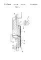
- FIG. 3 is an exploded perspective view of a thin film deposition apparatus according to the present invention.
- FIG. 4 is a perspective view of the shower head plate and the diffusion plate of FIG. 3;
- FIG. 5 is a vertical sectional view of the shower head plate shown in FIG. 3;
- a thin film deposition apparatus comprises a reactor block 10 for receiving a semiconductor wafer (not shown), and a shower head plate 20 hinged by hinges 29 a and 29 b .
- the shower head plate 20 covers the reactor block 10 to maintain the internal pressure of the reactor block 10 to a predetermined level.
- a diffusion plate 30 through which reaction gases are sprayed is installed in the shower head plate 20 , and the diffusion plate 30 is placed in the reactor block 10 when the reactor block 10 is covered by the shower head plate 20 .
- a shield 25 serving to minimize the area exposed to the reaction gases is detachably installed in the reactor block 10 .
- the shield 25 is formed of alumina, aluminum or stainless steel, and is installed very closely to the inner wall of the reactor block 10 .
- a wall of inert gas is lowered along the inner wall of the shield 25 .
- the reaction gases flow through the first pipe 11 and the first connection pipe 21 , or the second pipe 12 and the second connection pipe 22 , and are finally sprayed into the reactor block 10 through spray holes 33 of the diffusion plate 30 .
- the inert gas flows through the third pipe 13 , the third connection pipe 23 and the passages 32 in sequence and is then sprayed into the reactor block 10 through the nozzles 31 , lowering a wall of inert gas along the inner wall of the shield 25 .
- the wall of inert gas prevents the reaction gases from contacting the shield 25 .
- the anti-flow cylinder 27 a and the evenly distributed spray holes 33 allow a laminar flow of reaction gases over a wafer, and the reaction gases and the inert gas sprayed by the diffusion plate 30 into the reactor block 10 are discharged through the symmetrically placed exhaust holes 28 and the reactor exhaust holes 18 .
- reaction gases and the inert gas are evenly discharged through the symmetrically arranged discharge holes, thereby allowing different gas to continuously flow in.
Abstract
Description
Claims (7)
Applications Claiming Priority (2)
| Application Number | Priority Date | Filing Date | Title |
|---|---|---|---|
| KR98-17858 | 1998-05-18 | ||
| KR1019980017858A KR100267885B1 (en) | 1998-05-18 | 1998-05-18 | Deposition apparatus |
Publications (1)
| Publication Number | Publication Date |
|---|---|
| US6183563B1 true US6183563B1 (en) | 2001-02-06 |
Family
ID=36580479
Family Applications (1)
| Application Number | Title | Priority Date | Filing Date |
|---|---|---|---|
| US09/313,765 Expired - Lifetime US6183563B1 (en) | 1998-05-18 | 1999-05-18 | Apparatus for depositing thin films on semiconductor wafers |
Country Status (6)
| Country | Link |
|---|---|
| US (1) | US6183563B1 (en) |
| EP (1) | EP0959150B8 (en) |
| JP (1) | JP3073489B2 (en) |
| KR (1) | KR100267885B1 (en) |
| DE (1) | DE69927548T2 (en) |
| TW (1) | TW483051B (en) |
Cited By (103)
| Publication number | Priority date | Publication date | Assignee | Title |
|---|---|---|---|---|
| US20020007790A1 (en) * | 2000-07-22 | 2002-01-24 | Park Young-Hoon | Atomic layer deposition (ALD) thin film deposition equipment having cleaning apparatus and cleaning method |
| US20030079686A1 (en) * | 2001-10-26 | 2003-05-01 | Ling Chen | Gas delivery apparatus and method for atomic layer deposition |
| US20030106490A1 (en) * | 2001-12-06 | 2003-06-12 | Applied Materials, Inc. | Apparatus and method for fast-cycle atomic layer deposition |
| US6579373B2 (en) * | 2001-10-23 | 2003-06-17 | Tokyo Electron Limited | Substrate processing apparatus and substrate processing method |
| US20030121608A1 (en) * | 2001-10-26 | 2003-07-03 | Applied Materials, Inc. | Gas delivery apparatus for atomic layer deposition |
| US20030143841A1 (en) * | 2002-01-26 | 2003-07-31 | Yang Michael X. | Integration of titanium and titanium nitride layers |
| US20030198740A1 (en) * | 2001-10-05 | 2003-10-23 | Applied Materials, Inc. | Apparatus and method for evenly flowing processing gas onto a semiconductor wafer |
| US20030198754A1 (en) * | 2001-07-16 | 2003-10-23 | Ming Xi | Aluminum oxide chamber and process |
| US20030224600A1 (en) * | 2002-03-04 | 2003-12-04 | Wei Cao | Sequential deposition of tantalum nitride using a tantalum-containing precursor and a nitrogen-containing precursor |
| US20030221780A1 (en) * | 2002-01-26 | 2003-12-04 | Lei Lawrence C. | Clamshell and small volume chamber with fixed substrate support |
| US6660126B2 (en) * | 2001-03-02 | 2003-12-09 | Applied Materials, Inc. | Lid assembly for a processing system to facilitate sequential deposition techniques |
| US20040011404A1 (en) * | 2002-07-19 | 2004-01-22 | Ku Vincent W | Valve design and configuration for fast delivery system |
| US20040062865A1 (en) * | 2001-12-20 | 2004-04-01 | Wheat Gary E. | Gas distributor for vapor coating method and container |
| US6718126B2 (en) | 2001-09-14 | 2004-04-06 | Applied Materials, Inc. | Apparatus and method for vaporizing solid precursor for CVD or atomic layer deposition |
| US20040065255A1 (en) * | 2002-10-02 | 2004-04-08 | Applied Materials, Inc. | Cyclical layer deposition system |
| US20040071897A1 (en) * | 2002-10-11 | 2004-04-15 | Applied Materials, Inc. | Activated species generator for rapid cycle deposition processes |
| US20040069227A1 (en) * | 2002-10-09 | 2004-04-15 | Applied Materials, Inc. | Processing chamber configured for uniform gas flow |
| US6729824B2 (en) | 2001-12-14 | 2004-05-04 | Applied Materials, Inc. | Dual robot processing system |
| US6765178B2 (en) | 2000-12-29 | 2004-07-20 | Applied Materials, Inc. | Chamber for uniform substrate heating |
| US20040144431A1 (en) * | 2003-01-29 | 2004-07-29 | Joseph Yudovsky | Rotary gas valve for pulsing a gas |
| US20040144311A1 (en) * | 2002-11-14 | 2004-07-29 | Ling Chen | Apparatus and method for hybrid chemical processing |
| US20040144308A1 (en) * | 2003-01-29 | 2004-07-29 | Applied Materials, Inc. | Membrane gas valve for pulsing a gas |
| US6772072B2 (en) | 2002-07-22 | 2004-08-03 | Applied Materials, Inc. | Method and apparatus for monitoring solid precursor delivery |
| US20040187779A1 (en) * | 2003-03-27 | 2004-09-30 | Park Young Hoon | Thin film deposition reactor |
| US20040187780A1 (en) * | 2003-03-31 | 2004-09-30 | Park Young Hoon | Thin film deposition reactor |
| US20040211665A1 (en) * | 2001-07-25 | 2004-10-28 | Yoon Ki Hwan | Barrier formation using novel sputter-deposition method |
| US20040226507A1 (en) * | 2003-04-24 | 2004-11-18 | Carpenter Craig M. | Methods for controlling mass flow rates and pressures in passageways coupled to reaction chambers and systems for depositing material onto microfeature workpieces in reaction chambers |
| US6821563B2 (en) | 2002-10-02 | 2004-11-23 | Applied Materials, Inc. | Gas distribution system for cyclical layer deposition |
| US6825447B2 (en) | 2000-12-29 | 2004-11-30 | Applied Materials, Inc. | Apparatus and method for uniform substrate heating and contaminate collection |
| US20050000423A1 (en) * | 2001-02-09 | 2005-01-06 | Shigeru Kasai | Film forming device |
| US20050014382A1 (en) * | 2003-07-16 | 2005-01-20 | Samsung Electronics Co., Ltd. | Etching apparatus and method |
| US20050016984A1 (en) * | 2002-08-15 | 2005-01-27 | Dando Ross S. | Reactors with isolated gas connectors and methods for depositing materials onto micro-device workpieces |
| US6849545B2 (en) | 2001-06-20 | 2005-02-01 | Applied Materials, Inc. | System and method to form a composite film stack utilizing sequential deposition techniques |
| US20050022739A1 (en) * | 2002-07-08 | 2005-02-03 | Carpenter Craig M. | Apparatus and method for depositing materials onto microelectronic workpieces |
| US20050028734A1 (en) * | 2003-02-11 | 2005-02-10 | Carpenter Craig M. | Reactors with isolated gas connectors and methods for depositing materials onto micro-device workpieces |
| US20050039680A1 (en) * | 2003-08-21 | 2005-02-24 | Beaman Kevin L. | Methods and apparatus for processing microfeature workpieces; methods for conditioning ALD reaction chambers |
| US20050045102A1 (en) * | 2003-08-28 | 2005-03-03 | Zheng Lingyi A. | Methods and apparatus for processing microfeature workpieces, e.g., for depositing materials on microfeature workpieces |
| US20050067103A1 (en) * | 2003-09-26 | 2005-03-31 | Applied Materials, Inc. | Interferometer endpoint monitoring device |
| US20050087302A1 (en) * | 2003-10-10 | 2005-04-28 | Mardian Allen P. | Apparatus and methods for manufacturing microfeatures on workpieces using plasma vapor processes |
| US20050087130A1 (en) * | 2003-10-09 | 2005-04-28 | Derderian Garo J. | Apparatus and methods for plasma vapor deposition processes |
| US20050095859A1 (en) * | 2003-11-03 | 2005-05-05 | Applied Materials, Inc. | Precursor delivery system with rate control |
| US20050115675A1 (en) * | 2001-07-16 | 2005-06-02 | Gwo-Chuan Tzu | Lid assembly for a processing system to facilitate sequential deposition techniques |
| US20050139948A1 (en) * | 2001-09-26 | 2005-06-30 | Applied Materials, Inc. | Integration of barrier layer and seed layer |
| US6915592B2 (en) | 2002-07-29 | 2005-07-12 | Applied Materials, Inc. | Method and apparatus for generating gas to a processing chamber |
| US20050175789A1 (en) * | 2002-06-23 | 2005-08-11 | Helms Jr Aubrey L. | Method for energy-assisted atomic layer deposition and removal |
| US20050183827A1 (en) * | 2004-02-24 | 2005-08-25 | Applied Materials, Inc. | Showerhead mounting to accommodate thermal expansion |
| US20050189072A1 (en) * | 2002-07-17 | 2005-09-01 | Applied Materials, Inc. | Method and apparatus of generating PDMAT precursor |
| US20050209783A1 (en) * | 1996-12-20 | 2005-09-22 | Bittleston Simon H | Control devices for controlling the position of a marine seismic streamer |
| US6955211B2 (en) | 2002-07-17 | 2005-10-18 | Applied Materials, Inc. | Method and apparatus for gas temperature control in a semiconductor processing system |
| US20050249887A1 (en) * | 2004-05-06 | 2005-11-10 | Dando Ross S | Methods for depositing material onto microfeature workpieces in reaction chambers and systems for depositing materials onto microfeature workpieces |
| US20050249873A1 (en) * | 2004-05-05 | 2005-11-10 | Demetrius Sarigiannis | Apparatuses and methods for producing chemically reactive vapors used in manufacturing microelectronic devices |
| US20050252449A1 (en) * | 2004-05-12 | 2005-11-17 | Nguyen Son T | Control of gas flow and delivery to suppress the formation of particles in an MOCVD/ALD system |
| US20050260357A1 (en) * | 2004-05-21 | 2005-11-24 | Applied Materials, Inc. | Stabilization of high-k dielectric materials |
| US20050260347A1 (en) * | 2004-05-21 | 2005-11-24 | Narwankar Pravin K | Formation of a silicon oxynitride layer on a high-k dielectric material |
| US20060019033A1 (en) * | 2004-05-21 | 2006-01-26 | Applied Materials, Inc. | Plasma treatment of hafnium-containing materials |
| US20060075966A1 (en) * | 2002-01-26 | 2006-04-13 | Applied Materials, Inc. | Apparatus and method for plasma assisted deposition |
| US20060148253A1 (en) * | 2001-09-26 | 2006-07-06 | Applied Materials, Inc. | Integration of ALD tantalum nitride for copper metallization |
| US20060153995A1 (en) * | 2004-05-21 | 2006-07-13 | Applied Materials, Inc. | Method for fabricating a dielectric stack |
| US20060223286A1 (en) * | 2001-07-27 | 2006-10-05 | Chin Barry L | Atomic layer deposition apparatus |
| US7175713B2 (en) | 2002-01-25 | 2007-02-13 | Applied Materials, Inc. | Apparatus for cyclical deposition of thin films |
| US20070049053A1 (en) * | 2005-08-26 | 2007-03-01 | Applied Materials, Inc. | Pretreatment processes within a batch ALD reactor |
| US20070049043A1 (en) * | 2005-08-23 | 2007-03-01 | Applied Materials, Inc. | Nitrogen profile engineering in HI-K nitridation for device performance enhancement and reliability improvement |
| US20070065578A1 (en) * | 2005-09-21 | 2007-03-22 | Applied Materials, Inc. | Treatment processes for a batch ALD reactor |
| US20070079759A1 (en) * | 2005-10-07 | 2007-04-12 | Applied Materials, Inc. | Ampoule splash guard apparatus |
| US20070119371A1 (en) * | 2005-11-04 | 2007-05-31 | Paul Ma | Apparatus and process for plasma-enhanced atomic layer deposition |
| US20070169373A1 (en) * | 2006-01-25 | 2007-07-26 | Tokyo Electron Limited | Heat processing apparatus and heat processing method |
| US20070202254A1 (en) * | 2001-07-25 | 2007-08-30 | Seshadri Ganguli | Process for forming cobalt-containing materials |
| US20070252299A1 (en) * | 2006-04-27 | 2007-11-01 | Applied Materials, Inc. | Synchronization of precursor pulsing and wafer rotation |
| US20070259110A1 (en) * | 2006-05-05 | 2007-11-08 | Applied Materials, Inc. | Plasma, uv and ion/neutral assisted ald or cvd in a batch tool |
| US20070259111A1 (en) * | 2006-05-05 | 2007-11-08 | Singh Kaushal K | Method and apparatus for photo-excitation of chemicals for atomic layer deposition of dielectric film |
| US20080044595A1 (en) * | 2005-07-19 | 2008-02-21 | Randhir Thakur | Method for semiconductor processing |
| US7342984B1 (en) | 2003-04-03 | 2008-03-11 | Zilog, Inc. | Counting clock cycles over the duration of a first character and using a remainder value to determine when to sample a bit of a second character |
| US20080099933A1 (en) * | 2006-10-31 | 2008-05-01 | Choi Kenric T | Ampoule for liquid draw and vapor draw with a continous level sensor |
| US20080099145A1 (en) * | 2005-09-02 | 2008-05-01 | Applied Materials, Inc. | Gas sealing skirt for suspended showerhead in process chamber |
| US20080099436A1 (en) * | 2006-10-30 | 2008-05-01 | Michael Grimbergen | Endpoint detection for photomask etching |
| US20080099146A1 (en) * | 2006-10-25 | 2008-05-01 | Applied Materials, Inc. | Suspension for showerhead in process chamber |
| US20080176149A1 (en) * | 2006-10-30 | 2008-07-24 | Applied Materials, Inc. | Endpoint detection for photomask etching |
| US20080202425A1 (en) * | 2007-01-29 | 2008-08-28 | Applied Materials, Inc. | Temperature controlled lid assembly for tungsten nitride deposition |
| US20080268636A1 (en) * | 2001-07-25 | 2008-10-30 | Ki Hwan Yoon | Deposition methods for barrier and tungsten materials |
| US20080268635A1 (en) * | 2001-07-25 | 2008-10-30 | Sang-Ho Yu | Process for forming cobalt and cobalt silicide materials in copper contact applications |
| US20090053426A1 (en) * | 2001-07-25 | 2009-02-26 | Jiang Lu | Cobalt deposition on barrier surfaces |
| US20090101069A1 (en) * | 2007-10-12 | 2009-04-23 | Suhail Anwar | Rf return plates for backing plate support |
| US7547952B2 (en) | 2003-04-04 | 2009-06-16 | Applied Materials, Inc. | Method for hafnium nitride deposition |
| US7601648B2 (en) | 2006-07-31 | 2009-10-13 | Applied Materials, Inc. | Method for fabricating an integrated gate dielectric layer for field effect transistors |
| US7699932B2 (en) | 2004-06-02 | 2010-04-20 | Micron Technology, Inc. | Reactors, systems and methods for depositing thin films onto microfeature workpieces |
| US20100112215A1 (en) * | 2008-10-31 | 2010-05-06 | Applied Materials, Inc. | Chemical precursor ampoule for vapor deposition processes |
| US7871470B2 (en) | 2003-03-12 | 2011-01-18 | Applied Materials, Inc. | Substrate support lift mechanism |
| US20110086509A1 (en) * | 2001-07-25 | 2011-04-14 | Seshadri Ganguli | Process for forming cobalt and cobalt silicide materials in tungsten contact applications |
| US20130344245A1 (en) * | 2012-06-25 | 2013-12-26 | Novellus Systems, Inc. | Suppression of parasitic deposition in a substrate processing system by suppressing precursor flow and plasma outside of substrate region |
| US20140090599A1 (en) * | 2012-09-28 | 2014-04-03 | Tokyo Electron Limited | Film forming apparatus |
| US8778574B2 (en) | 2012-11-30 | 2014-07-15 | Applied Materials, Inc. | Method for etching EUV material layers utilized to form a photomask |
| US8778204B2 (en) | 2010-10-29 | 2014-07-15 | Applied Materials, Inc. | Methods for reducing photoresist interference when monitoring a target layer in a plasma process |
| US8808559B2 (en) | 2011-11-22 | 2014-08-19 | Applied Materials, Inc. | Etch rate detection for reflective multi-material layers etching |
| JP2014192473A (en) * | 2013-03-28 | 2014-10-06 | Disco Abrasive Syst Ltd | Wafer sticking device |
| US8900469B2 (en) | 2011-12-19 | 2014-12-02 | Applied Materials, Inc. | Etch rate detection for anti-reflective coating layer and absorber layer etching |
| US8961804B2 (en) | 2011-10-25 | 2015-02-24 | Applied Materials, Inc. | Etch rate detection for photomask etching |
| CN105420687A (en) * | 2016-01-04 | 2016-03-23 | 厦门市三安光电科技有限公司 | MOCVD system |
| US9399228B2 (en) | 2013-02-06 | 2016-07-26 | Novellus Systems, Inc. | Method and apparatus for purging and plasma suppression in a process chamber |
| US9758868B1 (en) | 2016-03-10 | 2017-09-12 | Lam Research Corporation | Plasma suppression behind a showerhead through the use of increased pressure |
| US9805939B2 (en) | 2012-10-12 | 2017-10-31 | Applied Materials, Inc. | Dual endpoint detection for advanced phase shift and binary photomasks |
| US9909213B2 (en) * | 2013-08-12 | 2018-03-06 | Applied Materials, Inc. | Recursive pumping for symmetrical gas exhaust to control critical dimension uniformity in plasma reactors |
| US10464092B2 (en) * | 2013-05-03 | 2019-11-05 | Oerlikon Metco Ag, Wohlen | Processing apparatus for processing a workpiece surface with fluid flow shielding |
| CN113832448A (en) * | 2020-06-23 | 2021-12-24 | 拓荆科技股份有限公司 | Semiconductor film deposition equipment and semiconductor film coating method |
Families Citing this family (9)
| Publication number | Priority date | Publication date | Assignee | Title |
|---|---|---|---|---|
| DE19959603A1 (en) * | 1999-12-10 | 2001-06-13 | Volkswagen Ag | Process for coating the inner surface and/or the components of a reactor vessel comprises introducing a gas mixture containing a titanium dispenser and a nitrogen dispenser and depositing titanium nitride onto the surface and/or components |
| DE19959604A1 (en) * | 1999-12-10 | 2001-06-13 | Volkswagen Ag | Reactor for plasma deposition and plasma diffusion processes comprises a closed or closable reactor vessel whose inner side is coated with a titanium nitride layer |
| KR100332314B1 (en) * | 2000-06-24 | 2002-04-12 | 서성기 | Reactor for depositing thin film on wafer |
| KR100423953B1 (en) * | 2001-03-19 | 2004-03-24 | 디지웨이브 테크놀러지스 주식회사 | Chemical Vapor Deposition Apparatus |
| WO2003038145A2 (en) * | 2001-10-29 | 2003-05-08 | Genus, Inc. | Chemical vapor deposition system |
| JP2003197532A (en) * | 2001-12-21 | 2003-07-11 | Sumitomo Mitsubishi Silicon Corp | Epitaxial growth method and epitaxial growth suscepter |
| US20050000449A1 (en) | 2001-12-21 | 2005-01-06 | Masayuki Ishibashi | Susceptor for epitaxial growth and epitaxial growth method |
| US7118781B1 (en) * | 2003-04-16 | 2006-10-10 | Cree, Inc. | Methods for controlling formation of deposits in a deposition system and deposition methods including the same |
| GB2415707A (en) | 2004-06-30 | 2006-01-04 | Arima Optoelectronic | Vertical hydride vapour phase epitaxy deposition using a homogenising diaphragm |
Citations (9)
| Publication number | Priority date | Publication date | Assignee | Title |
|---|---|---|---|---|
| JPH0246723A (en) * | 1988-08-09 | 1990-02-16 | Fujitsu Ltd | Device for thin film formation |
| US5000113A (en) * | 1986-12-19 | 1991-03-19 | Applied Materials, Inc. | Thermal CVD/PECVD reactor and use for thermal chemical vapor deposition of silicon dioxide and in-situ multi-step planarized process |
| US5010842A (en) * | 1988-10-25 | 1991-04-30 | Mitsubishi Denki Kabushiki Kaisha | Apparatus for forming thin film |
| US5522932A (en) * | 1993-05-14 | 1996-06-04 | Applied Materials, Inc. | Corrosion-resistant apparatus |
| US5558717A (en) * | 1994-11-30 | 1996-09-24 | Applied Materials | CVD Processing chamber |
| US5788747A (en) * | 1996-01-24 | 1998-08-04 | Tokyo Electron Limited | Exhaust system for film forming apparatus |
| US5900103A (en) * | 1994-04-20 | 1999-05-04 | Tokyo Electron Limited | Plasma treatment method and apparatus |
| US5906683A (en) * | 1996-04-16 | 1999-05-25 | Applied Materials, Inc. | Lid assembly for semiconductor processing chamber |
| US5968276A (en) * | 1997-07-11 | 1999-10-19 | Applied Materials, Inc. | Heat exchange passage connection |
Family Cites Families (3)
| Publication number | Priority date | Publication date | Assignee | Title |
|---|---|---|---|---|
| JP2701363B2 (en) * | 1988-09-12 | 1998-01-21 | 三菱電機株式会社 | Semiconductor device manufacturing method and thin film forming apparatus used therefor |
| JP2763222B2 (en) * | 1991-12-13 | 1998-06-11 | 三菱電機株式会社 | Chemical vapor deposition method, chemical vapor deposition processing system and chemical vapor deposition apparatus therefor |
| EP0854210B1 (en) * | 1996-12-19 | 2002-03-27 | Toshiba Ceramics Co., Ltd. | Vapor deposition apparatus for forming thin film |
-
1998
- 1998-05-18 KR KR1019980017858A patent/KR100267885B1/en not_active IP Right Cessation
-
1999
- 1999-05-17 TW TW088107958A patent/TW483051B/en not_active IP Right Cessation
- 1999-05-18 JP JP11136866A patent/JP3073489B2/en not_active Expired - Lifetime
- 1999-05-18 US US09/313,765 patent/US6183563B1/en not_active Expired - Lifetime
- 1999-05-18 DE DE69927548T patent/DE69927548T2/en not_active Expired - Fee Related
- 1999-05-18 EP EP99303880A patent/EP0959150B8/en not_active Expired - Lifetime
Patent Citations (9)
| Publication number | Priority date | Publication date | Assignee | Title |
|---|---|---|---|---|
| US5000113A (en) * | 1986-12-19 | 1991-03-19 | Applied Materials, Inc. | Thermal CVD/PECVD reactor and use for thermal chemical vapor deposition of silicon dioxide and in-situ multi-step planarized process |
| JPH0246723A (en) * | 1988-08-09 | 1990-02-16 | Fujitsu Ltd | Device for thin film formation |
| US5010842A (en) * | 1988-10-25 | 1991-04-30 | Mitsubishi Denki Kabushiki Kaisha | Apparatus for forming thin film |
| US5522932A (en) * | 1993-05-14 | 1996-06-04 | Applied Materials, Inc. | Corrosion-resistant apparatus |
| US5900103A (en) * | 1994-04-20 | 1999-05-04 | Tokyo Electron Limited | Plasma treatment method and apparatus |
| US5558717A (en) * | 1994-11-30 | 1996-09-24 | Applied Materials | CVD Processing chamber |
| US5788747A (en) * | 1996-01-24 | 1998-08-04 | Tokyo Electron Limited | Exhaust system for film forming apparatus |
| US5906683A (en) * | 1996-04-16 | 1999-05-25 | Applied Materials, Inc. | Lid assembly for semiconductor processing chamber |
| US5968276A (en) * | 1997-07-11 | 1999-10-19 | Applied Materials, Inc. | Heat exchange passage connection |
Cited By (222)
| Publication number | Priority date | Publication date | Assignee | Title |
|---|---|---|---|---|
| US20050209783A1 (en) * | 1996-12-20 | 2005-09-22 | Bittleston Simon H | Control devices for controlling the position of a marine seismic streamer |
| US6796316B2 (en) * | 2000-07-22 | 2004-09-28 | Ips Ltd. | Atomic layer deposition (ALD) thin film deposition equipment having cleaning apparatus and cleaning method |
| US20020007790A1 (en) * | 2000-07-22 | 2002-01-24 | Park Young-Hoon | Atomic layer deposition (ALD) thin film deposition equipment having cleaning apparatus and cleaning method |
| US6825447B2 (en) | 2000-12-29 | 2004-11-30 | Applied Materials, Inc. | Apparatus and method for uniform substrate heating and contaminate collection |
| US6765178B2 (en) | 2000-12-29 | 2004-07-20 | Applied Materials, Inc. | Chamber for uniform substrate heating |
| US8128751B2 (en) | 2001-02-09 | 2012-03-06 | Tokyo Electron Limited | Film-forming apparatus |
| US20050000423A1 (en) * | 2001-02-09 | 2005-01-06 | Shigeru Kasai | Film forming device |
| US20100107977A1 (en) * | 2001-02-09 | 2010-05-06 | Tokyo Electron Limited | Film forming apparatus |
| US7661386B2 (en) | 2001-02-09 | 2010-02-16 | Tokyo Electron Limited | Film forming device |
| US20090178614A1 (en) * | 2001-02-09 | 2009-07-16 | Tokyo Electron Limited | Film-forming apparatus |
| US9587310B2 (en) | 2001-03-02 | 2017-03-07 | Applied Materials, Inc. | Lid assembly for a processing system to facilitate sequential deposition techniques |
| US6660126B2 (en) * | 2001-03-02 | 2003-12-09 | Applied Materials, Inc. | Lid assembly for a processing system to facilitate sequential deposition techniques |
| US6849545B2 (en) | 2001-06-20 | 2005-02-01 | Applied Materials, Inc. | System and method to form a composite film stack utilizing sequential deposition techniques |
| US20110114020A1 (en) * | 2001-07-16 | 2011-05-19 | Gwo-Chuan Tzu | Lid assembly for a processing system to facilitate sequential deposition techniques |
| US10280509B2 (en) | 2001-07-16 | 2019-05-07 | Applied Materials, Inc. | Lid assembly for a processing system to facilitate sequential deposition techniques |
| US7905959B2 (en) | 2001-07-16 | 2011-03-15 | Applied Materials, Inc. | Lid assembly for a processing system to facilitate sequential deposition techniques |
| US20030198754A1 (en) * | 2001-07-16 | 2003-10-23 | Ming Xi | Aluminum oxide chamber and process |
| US20050115675A1 (en) * | 2001-07-16 | 2005-06-02 | Gwo-Chuan Tzu | Lid assembly for a processing system to facilitate sequential deposition techniques |
| US20080268636A1 (en) * | 2001-07-25 | 2008-10-30 | Ki Hwan Yoon | Deposition methods for barrier and tungsten materials |
| US20110086509A1 (en) * | 2001-07-25 | 2011-04-14 | Seshadri Ganguli | Process for forming cobalt and cobalt silicide materials in tungsten contact applications |
| US9051641B2 (en) | 2001-07-25 | 2015-06-09 | Applied Materials, Inc. | Cobalt deposition on barrier surfaces |
| US20090053426A1 (en) * | 2001-07-25 | 2009-02-26 | Jiang Lu | Cobalt deposition on barrier surfaces |
| US20070202254A1 (en) * | 2001-07-25 | 2007-08-30 | Seshadri Ganguli | Process for forming cobalt-containing materials |
| US8110489B2 (en) | 2001-07-25 | 2012-02-07 | Applied Materials, Inc. | Process for forming cobalt-containing materials |
| US8563424B2 (en) | 2001-07-25 | 2013-10-22 | Applied Materials, Inc. | Process for forming cobalt and cobalt silicide materials in tungsten contact applications |
| US20080268635A1 (en) * | 2001-07-25 | 2008-10-30 | Sang-Ho Yu | Process for forming cobalt and cobalt silicide materials in copper contact applications |
| US20040211665A1 (en) * | 2001-07-25 | 2004-10-28 | Yoon Ki Hwan | Barrier formation using novel sputter-deposition method |
| US7416979B2 (en) | 2001-07-25 | 2008-08-26 | Applied Materials, Inc. | Deposition methods for barrier and tungsten materials |
| US9209074B2 (en) | 2001-07-25 | 2015-12-08 | Applied Materials, Inc. | Cobalt deposition on barrier surfaces |
| US8187970B2 (en) | 2001-07-25 | 2012-05-29 | Applied Materials, Inc. | Process for forming cobalt and cobalt silicide materials in tungsten contact applications |
| US9031685B2 (en) | 2001-07-27 | 2015-05-12 | Applied Materials, Inc. | Atomic layer deposition apparatus |
| US7860597B2 (en) | 2001-07-27 | 2010-12-28 | Applied Materials, Inc. | Atomic layer deposition apparatus |
| US20100099270A1 (en) * | 2001-07-27 | 2010-04-22 | Chin Barry L | Atomic layer deposition apparatus |
| US8626330B2 (en) | 2001-07-27 | 2014-01-07 | Applied Materials, Inc. | Atomic layer deposition apparatus |
| US7660644B2 (en) | 2001-07-27 | 2010-02-09 | Applied Materials, Inc. | Atomic layer deposition apparatus |
| US20110111603A1 (en) * | 2001-07-27 | 2011-05-12 | Chin Barry L | Atomic layer deposition apparatus |
| US8027746B2 (en) | 2001-07-27 | 2011-09-27 | Applied Materials, Inc. | Atomic layer deposition apparatus |
| US20060223286A1 (en) * | 2001-07-27 | 2006-10-05 | Chin Barry L | Atomic layer deposition apparatus |
| US6718126B2 (en) | 2001-09-14 | 2004-04-06 | Applied Materials, Inc. | Apparatus and method for vaporizing solid precursor for CVD or atomic layer deposition |
| US20040170403A1 (en) * | 2001-09-14 | 2004-09-02 | Applied Materials, Inc. | Apparatus and method for vaporizing solid precursor for CVD or atomic layer deposition |
| US20060148253A1 (en) * | 2001-09-26 | 2006-07-06 | Applied Materials, Inc. | Integration of ALD tantalum nitride for copper metallization |
| US20070283886A1 (en) * | 2001-09-26 | 2007-12-13 | Hua Chung | Apparatus for integration of barrier layer and seed layer |
| US20050139948A1 (en) * | 2001-09-26 | 2005-06-30 | Applied Materials, Inc. | Integration of barrier layer and seed layer |
| US20030198740A1 (en) * | 2001-10-05 | 2003-10-23 | Applied Materials, Inc. | Apparatus and method for evenly flowing processing gas onto a semiconductor wafer |
| US6797108B2 (en) | 2001-10-05 | 2004-09-28 | Applied Materials, Inc. | Apparatus and method for evenly flowing processing gas onto a semiconductor wafer |
| US6713405B2 (en) | 2001-10-23 | 2004-03-30 | Tokyo Electron Limited | Substrate processing apparatus and substrate processing method |
| US6579373B2 (en) * | 2001-10-23 | 2003-06-17 | Tokyo Electron Limited | Substrate processing apparatus and substrate processing method |
| US20100247767A1 (en) * | 2001-10-26 | 2010-09-30 | Ling Chen | Gas delivery apparatus and method for atomic layer deposition |
| US7780788B2 (en) | 2001-10-26 | 2010-08-24 | Applied Materials, Inc. | Gas delivery apparatus for atomic layer deposition |
| US7780785B2 (en) | 2001-10-26 | 2010-08-24 | Applied Materials, Inc. | Gas delivery apparatus for atomic layer deposition |
| US8668776B2 (en) | 2001-10-26 | 2014-03-11 | Applied Materials, Inc. | Gas delivery apparatus and method for atomic layer deposition |
| US20030121608A1 (en) * | 2001-10-26 | 2003-07-03 | Applied Materials, Inc. | Gas delivery apparatus for atomic layer deposition |
| US20050173068A1 (en) * | 2001-10-26 | 2005-08-11 | Ling Chen | Gas delivery apparatus and method for atomic layer deposition |
| US20030124262A1 (en) * | 2001-10-26 | 2003-07-03 | Ling Chen | Integration of ALD tantalum nitride and alpha-phase tantalum for copper metallization application |
| US20030079686A1 (en) * | 2001-10-26 | 2003-05-01 | Ling Chen | Gas delivery apparatus and method for atomic layer deposition |
| US20030106490A1 (en) * | 2001-12-06 | 2003-06-12 | Applied Materials, Inc. | Apparatus and method for fast-cycle atomic layer deposition |
| US6773507B2 (en) | 2001-12-06 | 2004-08-10 | Applied Materials, Inc. | Apparatus and method for fast-cycle atomic layer deposition |
| US6729824B2 (en) | 2001-12-14 | 2004-05-04 | Applied Materials, Inc. | Dual robot processing system |
| US6986814B2 (en) * | 2001-12-20 | 2006-01-17 | General Electric Company | Gas distributor for vapor coating method and container |
| US20040062865A1 (en) * | 2001-12-20 | 2004-04-01 | Wheat Gary E. | Gas distributor for vapor coating method and container |
| US8123860B2 (en) | 2002-01-25 | 2012-02-28 | Applied Materials, Inc. | Apparatus for cyclical depositing of thin films |
| US7175713B2 (en) | 2002-01-25 | 2007-02-13 | Applied Materials, Inc. | Apparatus for cyclical deposition of thin films |
| US20090056626A1 (en) * | 2002-01-25 | 2009-03-05 | Applied Materials, Inc. | Apparatus for cyclical depositing of thin films |
| US20070095285A1 (en) * | 2002-01-25 | 2007-05-03 | Thakur Randhir P | Apparatus for cyclical depositing of thin films |
| US7732325B2 (en) | 2002-01-26 | 2010-06-08 | Applied Materials, Inc. | Plasma-enhanced cyclic layer deposition process for barrier layers |
| US20030143841A1 (en) * | 2002-01-26 | 2003-07-31 | Yang Michael X. | Integration of titanium and titanium nitride layers |
| US20060292864A1 (en) * | 2002-01-26 | 2006-12-28 | Yang Michael X | Plasma-enhanced cyclic layer deposition process for barrier layers |
| US20060075966A1 (en) * | 2002-01-26 | 2006-04-13 | Applied Materials, Inc. | Apparatus and method for plasma assisted deposition |
| US6866746B2 (en) | 2002-01-26 | 2005-03-15 | Applied Materials, Inc. | Clamshell and small volume chamber with fixed substrate support |
| US20030221780A1 (en) * | 2002-01-26 | 2003-12-04 | Lei Lawrence C. | Clamshell and small volume chamber with fixed substrate support |
| US7779784B2 (en) | 2002-01-26 | 2010-08-24 | Applied Materials, Inc. | Apparatus and method for plasma assisted deposition |
| US20050139160A1 (en) * | 2002-01-26 | 2005-06-30 | Applied Materials, Inc. | Clamshell and small volume chamber with fixed substrate support |
| US6972267B2 (en) | 2002-03-04 | 2005-12-06 | Applied Materials, Inc. | Sequential deposition of tantalum nitride using a tantalum-containing precursor and a nitrogen-containing precursor |
| US20060019494A1 (en) * | 2002-03-04 | 2006-01-26 | Wei Cao | Sequential deposition of tantalum nitride using a tantalum-containing precursor and a nitrogen-containing precursor |
| US20030224600A1 (en) * | 2002-03-04 | 2003-12-04 | Wei Cao | Sequential deposition of tantalum nitride using a tantalum-containing precursor and a nitrogen-containing precursor |
| US7514358B2 (en) | 2002-03-04 | 2009-04-07 | Applied Materials, Inc. | Sequential deposition of tantalum nitride using a tantalum-containing precursor and a nitrogen-containing precursor |
| US7867896B2 (en) | 2002-03-04 | 2011-01-11 | Applied Materials, Inc. | Sequential deposition of tantalum nitride using a tantalum-containing precursor and a nitrogen-containing precursor |
| US20110070730A1 (en) * | 2002-03-04 | 2011-03-24 | Wei Cao | Sequential deposition of tantalum nitride using a tantalum-containing precursor and a nitrogen-containing precursor |
| US20050175789A1 (en) * | 2002-06-23 | 2005-08-11 | Helms Jr Aubrey L. | Method for energy-assisted atomic layer deposition and removal |
| US20050022739A1 (en) * | 2002-07-08 | 2005-02-03 | Carpenter Craig M. | Apparatus and method for depositing materials onto microelectronic workpieces |
| US20050189072A1 (en) * | 2002-07-17 | 2005-09-01 | Applied Materials, Inc. | Method and apparatus of generating PDMAT precursor |
| US20090011129A1 (en) * | 2002-07-17 | 2009-01-08 | Seshadri Ganguli | Method and apparatus for providing precursor gas to a processing chamber |
| US7588736B2 (en) | 2002-07-17 | 2009-09-15 | Applied Materials, Inc. | Apparatus and method for generating a chemical precursor |
| US7678194B2 (en) | 2002-07-17 | 2010-03-16 | Applied Materials, Inc. | Method for providing gas to a processing chamber |
| US6955211B2 (en) | 2002-07-17 | 2005-10-18 | Applied Materials, Inc. | Method and apparatus for gas temperature control in a semiconductor processing system |
| US7569191B2 (en) | 2002-07-17 | 2009-08-04 | Applied Materials, Inc. | Method and apparatus for providing precursor gas to a processing chamber |
| US20070110898A1 (en) * | 2002-07-17 | 2007-05-17 | Seshadri Ganguli | Method and apparatus for providing precursor gas to a processing chamber |
| US7270709B2 (en) | 2002-07-17 | 2007-09-18 | Applied Materials, Inc. | Method and apparatus of generating PDMAT precursor |
| US7597758B2 (en) | 2002-07-17 | 2009-10-06 | Applied Materials, Inc. | Chemical precursor ampoule for vapor deposition processes |
| US20060257295A1 (en) * | 2002-07-17 | 2006-11-16 | Ling Chen | Apparatus and method for generating a chemical precursor |
| US7429361B2 (en) | 2002-07-17 | 2008-09-30 | Applied Materials, Inc. | Method and apparatus for providing precursor gas to a processing chamber |
| US20040011404A1 (en) * | 2002-07-19 | 2004-01-22 | Ku Vincent W | Valve design and configuration for fast delivery system |
| US20060213557A1 (en) * | 2002-07-19 | 2006-09-28 | Ku Vincent W | Valve design and configuration for fast delivery system |
| US7228873B2 (en) | 2002-07-19 | 2007-06-12 | Applied Materials, Inc. | Valve design and configuration for fast delivery system |
| US7066194B2 (en) | 2002-07-19 | 2006-06-27 | Applied Materials, Inc. | Valve design and configuration for fast delivery system |
| US20060213558A1 (en) * | 2002-07-19 | 2006-09-28 | Applied Materials, Inc. | Valve design and configuration for fast delivery system |
| US6772072B2 (en) | 2002-07-22 | 2004-08-03 | Applied Materials, Inc. | Method and apparatus for monitoring solid precursor delivery |
| US7294208B2 (en) | 2002-07-29 | 2007-11-13 | Applied Materials, Inc. | Apparatus for providing gas to a processing chamber |
| US6915592B2 (en) | 2002-07-29 | 2005-07-12 | Applied Materials, Inc. | Method and apparatus for generating gas to a processing chamber |
| US20050257735A1 (en) * | 2002-07-29 | 2005-11-24 | Guenther Rolf A | Method and apparatus for providing gas to a processing chamber |
| US20050016984A1 (en) * | 2002-08-15 | 2005-01-27 | Dando Ross S. | Reactors with isolated gas connectors and methods for depositing materials onto micro-device workpieces |
| US7588804B2 (en) * | 2002-08-15 | 2009-09-15 | Micron Technology, Inc. | Reactors with isolated gas connectors and methods for depositing materials onto micro-device workpieces |
| US6821563B2 (en) | 2002-10-02 | 2004-11-23 | Applied Materials, Inc. | Gas distribution system for cyclical layer deposition |
| US20040065255A1 (en) * | 2002-10-02 | 2004-04-08 | Applied Materials, Inc. | Cyclical layer deposition system |
| US7422637B2 (en) | 2002-10-09 | 2008-09-09 | Applied Materials, Inc. | Processing chamber configured for uniform gas flow |
| US20040069227A1 (en) * | 2002-10-09 | 2004-04-15 | Applied Materials, Inc. | Processing chamber configured for uniform gas flow |
| US20070044719A1 (en) * | 2002-10-09 | 2007-03-01 | Applied Materials, Inc. | Processing chamber configured for uniform gas flow |
| US6905737B2 (en) | 2002-10-11 | 2005-06-14 | Applied Materials, Inc. | Method of delivering activated species for rapid cyclical deposition |
| US20060035025A1 (en) * | 2002-10-11 | 2006-02-16 | Applied Materials, Inc. | Activated species generator for rapid cycle deposition processes |
| US20040071897A1 (en) * | 2002-10-11 | 2004-04-15 | Applied Materials, Inc. | Activated species generator for rapid cycle deposition processes |
| US20070151514A1 (en) * | 2002-11-14 | 2007-07-05 | Ling Chen | Apparatus and method for hybrid chemical processing |
| US7204886B2 (en) | 2002-11-14 | 2007-04-17 | Applied Materials, Inc. | Apparatus and method for hybrid chemical processing |
| US20040144311A1 (en) * | 2002-11-14 | 2004-07-29 | Ling Chen | Apparatus and method for hybrid chemical processing |
| US7591907B2 (en) | 2002-11-14 | 2009-09-22 | Applied Materials, Inc. | Apparatus for hybrid chemical processing |
| US7402210B2 (en) | 2002-11-14 | 2008-07-22 | Applied Materials, Inc. | Apparatus and method for hybrid chemical processing |
| US20040144308A1 (en) * | 2003-01-29 | 2004-07-29 | Applied Materials, Inc. | Membrane gas valve for pulsing a gas |
| US6868859B2 (en) | 2003-01-29 | 2005-03-22 | Applied Materials, Inc. | Rotary gas valve for pulsing a gas |
| US20040144431A1 (en) * | 2003-01-29 | 2004-07-29 | Joseph Yudovsky | Rotary gas valve for pulsing a gas |
| US6994319B2 (en) | 2003-01-29 | 2006-02-07 | Applied Materials, Inc. | Membrane gas valve for pulsing a gas |
| US20050028734A1 (en) * | 2003-02-11 | 2005-02-10 | Carpenter Craig M. | Reactors with isolated gas connectors and methods for depositing materials onto micro-device workpieces |
| US7427425B2 (en) | 2003-02-11 | 2008-09-23 | Micron Technology, Inc. | Reactors with isolated gas connectors and methods for depositing materials onto micro-device workpieces |
| US7871470B2 (en) | 2003-03-12 | 2011-01-18 | Applied Materials, Inc. | Substrate support lift mechanism |
| US20040187779A1 (en) * | 2003-03-27 | 2004-09-30 | Park Young Hoon | Thin film deposition reactor |
| US20040187780A1 (en) * | 2003-03-31 | 2004-09-30 | Park Young Hoon | Thin film deposition reactor |
| US6884297B2 (en) * | 2003-03-31 | 2005-04-26 | Ips Ltd. | Thin film deposition reactor |
| US7342984B1 (en) | 2003-04-03 | 2008-03-11 | Zilog, Inc. | Counting clock cycles over the duration of a first character and using a remainder value to determine when to sample a bit of a second character |
| US7547952B2 (en) | 2003-04-04 | 2009-06-16 | Applied Materials, Inc. | Method for hafnium nitride deposition |
| US20040226507A1 (en) * | 2003-04-24 | 2004-11-18 | Carpenter Craig M. | Methods for controlling mass flow rates and pressures in passageways coupled to reaction chambers and systems for depositing material onto microfeature workpieces in reaction chambers |
| US20050014382A1 (en) * | 2003-07-16 | 2005-01-20 | Samsung Electronics Co., Ltd. | Etching apparatus and method |
| US20050039680A1 (en) * | 2003-08-21 | 2005-02-24 | Beaman Kevin L. | Methods and apparatus for processing microfeature workpieces; methods for conditioning ALD reaction chambers |
| US20050045102A1 (en) * | 2003-08-28 | 2005-03-03 | Zheng Lingyi A. | Methods and apparatus for processing microfeature workpieces, e.g., for depositing materials on microfeature workpieces |
| US7682984B2 (en) | 2003-09-26 | 2010-03-23 | Applied Materials, Inc. | Interferometer endpoint monitoring device |
| US20070023393A1 (en) * | 2003-09-26 | 2007-02-01 | Nguyen Khiem K | Interferometer endpoint monitoring device |
| US20050067103A1 (en) * | 2003-09-26 | 2005-03-31 | Applied Materials, Inc. | Interferometer endpoint monitoring device |
| US20050087130A1 (en) * | 2003-10-09 | 2005-04-28 | Derderian Garo J. | Apparatus and methods for plasma vapor deposition processes |
| US20050087302A1 (en) * | 2003-10-10 | 2005-04-28 | Mardian Allen P. | Apparatus and methods for manufacturing microfeatures on workpieces using plasma vapor processes |
| US20050095859A1 (en) * | 2003-11-03 | 2005-05-05 | Applied Materials, Inc. | Precursor delivery system with rate control |
| US20050183827A1 (en) * | 2004-02-24 | 2005-08-25 | Applied Materials, Inc. | Showerhead mounting to accommodate thermal expansion |
| US7722925B2 (en) | 2004-02-24 | 2010-05-25 | Applied Materials, Inc. | Showerhead mounting to accommodate thermal expansion |
| US20050249873A1 (en) * | 2004-05-05 | 2005-11-10 | Demetrius Sarigiannis | Apparatuses and methods for producing chemically reactive vapors used in manufacturing microelectronic devices |
| US8133554B2 (en) | 2004-05-06 | 2012-03-13 | Micron Technology, Inc. | Methods for depositing material onto microfeature workpieces in reaction chambers and systems for depositing materials onto microfeature workpieces |
| US9023436B2 (en) | 2004-05-06 | 2015-05-05 | Micron Technology, Inc. | Methods for depositing material onto microfeature workpieces in reaction chambers and systems for depositing materials onto microfeature workpieces |
| US20050249887A1 (en) * | 2004-05-06 | 2005-11-10 | Dando Ross S | Methods for depositing material onto microfeature workpieces in reaction chambers and systems for depositing materials onto microfeature workpieces |
| US8282992B2 (en) | 2004-05-12 | 2012-10-09 | Applied Materials, Inc. | Methods for atomic layer deposition of hafnium-containing high-K dielectric materials |
| US7794544B2 (en) | 2004-05-12 | 2010-09-14 | Applied Materials, Inc. | Control of gas flow and delivery to suppress the formation of particles in an MOCVD/ALD system |
| US20080044569A1 (en) * | 2004-05-12 | 2008-02-21 | Myo Nyi O | Methods for atomic layer deposition of hafnium-containing high-k dielectric materials |
| US20050271813A1 (en) * | 2004-05-12 | 2005-12-08 | Shreyas Kher | Apparatuses and methods for atomic layer deposition of hafnium-containing high-k dielectric materials |
| US20050252449A1 (en) * | 2004-05-12 | 2005-11-17 | Nguyen Son T | Control of gas flow and delivery to suppress the formation of particles in an MOCVD/ALD system |
| US8343279B2 (en) | 2004-05-12 | 2013-01-01 | Applied Materials, Inc. | Apparatuses for atomic layer deposition |
| US20050260357A1 (en) * | 2004-05-21 | 2005-11-24 | Applied Materials, Inc. | Stabilization of high-k dielectric materials |
| US8119210B2 (en) | 2004-05-21 | 2012-02-21 | Applied Materials, Inc. | Formation of a silicon oxynitride layer on a high-k dielectric material |
| US20060019033A1 (en) * | 2004-05-21 | 2006-01-26 | Applied Materials, Inc. | Plasma treatment of hafnium-containing materials |
| US20050260347A1 (en) * | 2004-05-21 | 2005-11-24 | Narwankar Pravin K | Formation of a silicon oxynitride layer on a high-k dielectric material |
| US8323754B2 (en) | 2004-05-21 | 2012-12-04 | Applied Materials, Inc. | Stabilization of high-k dielectric materials |
| US20060153995A1 (en) * | 2004-05-21 | 2006-07-13 | Applied Materials, Inc. | Method for fabricating a dielectric stack |
| US7699932B2 (en) | 2004-06-02 | 2010-04-20 | Micron Technology, Inc. | Reactors, systems and methods for depositing thin films onto microfeature workpieces |
| US20080044595A1 (en) * | 2005-07-19 | 2008-02-21 | Randhir Thakur | Method for semiconductor processing |
| US20070049043A1 (en) * | 2005-08-23 | 2007-03-01 | Applied Materials, Inc. | Nitrogen profile engineering in HI-K nitridation for device performance enhancement and reliability improvement |
| US20070049053A1 (en) * | 2005-08-26 | 2007-03-01 | Applied Materials, Inc. | Pretreatment processes within a batch ALD reactor |
| US20080261413A1 (en) * | 2005-08-26 | 2008-10-23 | Maitreyee Mahajani | Pretreatment processes within a batch ald reactor |
| US7972978B2 (en) | 2005-08-26 | 2011-07-05 | Applied Materials, Inc. | Pretreatment processes within a batch ALD reactor |
| US7402534B2 (en) | 2005-08-26 | 2008-07-22 | Applied Materials, Inc. | Pretreatment processes within a batch ALD reactor |
| US20080099145A1 (en) * | 2005-09-02 | 2008-05-01 | Applied Materials, Inc. | Gas sealing skirt for suspended showerhead in process chamber |
| US7641762B2 (en) | 2005-09-02 | 2010-01-05 | Applied Materials, Inc. | Gas sealing skirt for suspended showerhead in process chamber |
| US20070065578A1 (en) * | 2005-09-21 | 2007-03-22 | Applied Materials, Inc. | Treatment processes for a batch ALD reactor |
| US7464917B2 (en) | 2005-10-07 | 2008-12-16 | Appiled Materials, Inc. | Ampoule splash guard apparatus |
| US20070079759A1 (en) * | 2005-10-07 | 2007-04-12 | Applied Materials, Inc. | Ampoule splash guard apparatus |
| US20090114157A1 (en) * | 2005-10-07 | 2009-05-07 | Wei Ti Lee | Ampoule splash guard apparatus |
| US7699295B2 (en) | 2005-10-07 | 2010-04-20 | Applied Materials, Inc. | Ampoule splash guard apparatus |
| US20080268171A1 (en) * | 2005-11-04 | 2008-10-30 | Paul Ma | Apparatus and process for plasma-enhanced atomic layer deposition |
| US20070128864A1 (en) * | 2005-11-04 | 2007-06-07 | Paul Ma | Apparatus and process for plasma-enhanced atomic layer deposition |
| US20070128862A1 (en) * | 2005-11-04 | 2007-06-07 | Paul Ma | Apparatus and process for plasma-enhanced atomic layer deposition |
| US20070128863A1 (en) * | 2005-11-04 | 2007-06-07 | Paul Ma | Apparatus and process for plasma-enhanced atomic layer deposition |
| US7850779B2 (en) | 2005-11-04 | 2010-12-14 | Applied Materisals, Inc. | Apparatus and process for plasma-enhanced atomic layer deposition |
| US9032906B2 (en) | 2005-11-04 | 2015-05-19 | Applied Materials, Inc. | Apparatus and process for plasma-enhanced atomic layer deposition |
| US20070119370A1 (en) * | 2005-11-04 | 2007-05-31 | Paul Ma | Apparatus and process for plasma-enhanced atomic layer deposition |
| US7682946B2 (en) | 2005-11-04 | 2010-03-23 | Applied Materials, Inc. | Apparatus and process for plasma-enhanced atomic layer deposition |
| US20070119371A1 (en) * | 2005-11-04 | 2007-05-31 | Paul Ma | Apparatus and process for plasma-enhanced atomic layer deposition |
| US20070169373A1 (en) * | 2006-01-25 | 2007-07-26 | Tokyo Electron Limited | Heat processing apparatus and heat processing method |
| US8782918B2 (en) | 2006-01-25 | 2014-07-22 | Tokyo Electron Limited | Heat processing apparatus and heat processing method |
| US20110236845A1 (en) * | 2006-01-25 | 2011-09-29 | Tokyo Electron Limited | Heat processing apparatus and heat processing method |
| US7980003B2 (en) * | 2006-01-25 | 2011-07-19 | Tokyo Electron Limited | Heat processing apparatus and heat processing method |
| US20070252299A1 (en) * | 2006-04-27 | 2007-11-01 | Applied Materials, Inc. | Synchronization of precursor pulsing and wafer rotation |
| US7798096B2 (en) | 2006-05-05 | 2010-09-21 | Applied Materials, Inc. | Plasma, UV and ion/neutral assisted ALD or CVD in a batch tool |
| US20070259111A1 (en) * | 2006-05-05 | 2007-11-08 | Singh Kaushal K | Method and apparatus for photo-excitation of chemicals for atomic layer deposition of dielectric film |
| US20070259110A1 (en) * | 2006-05-05 | 2007-11-08 | Applied Materials, Inc. | Plasma, uv and ion/neutral assisted ald or cvd in a batch tool |
| US7601648B2 (en) | 2006-07-31 | 2009-10-13 | Applied Materials, Inc. | Method for fabricating an integrated gate dielectric layer for field effect transistors |
| US20080099146A1 (en) * | 2006-10-25 | 2008-05-01 | Applied Materials, Inc. | Suspension for showerhead in process chamber |
| US7776178B2 (en) | 2006-10-25 | 2010-08-17 | Applied Materials, Inc. | Suspension for showerhead in process chamber |
| US20090014409A1 (en) * | 2006-10-30 | 2009-01-15 | Michael Grimbergen | Endpoint detection for photomask etching |
| US20080176149A1 (en) * | 2006-10-30 | 2008-07-24 | Applied Materials, Inc. | Endpoint detection for photomask etching |
| US8092695B2 (en) | 2006-10-30 | 2012-01-10 | Applied Materials, Inc. | Endpoint detection for photomask etching |
| US20080099436A1 (en) * | 2006-10-30 | 2008-05-01 | Michael Grimbergen | Endpoint detection for photomask etching |
| US8158526B2 (en) | 2006-10-30 | 2012-04-17 | Applied Materials, Inc. | Endpoint detection for photomask etching |
| US20080099933A1 (en) * | 2006-10-31 | 2008-05-01 | Choi Kenric T | Ampoule for liquid draw and vapor draw with a continous level sensor |
| US7775508B2 (en) | 2006-10-31 | 2010-08-17 | Applied Materials, Inc. | Ampoule for liquid draw and vapor draw with a continuous level sensor |
| US8821637B2 (en) | 2007-01-29 | 2014-09-02 | Applied Materials, Inc. | Temperature controlled lid assembly for tungsten nitride deposition |
| US20080202425A1 (en) * | 2007-01-29 | 2008-08-28 | Applied Materials, Inc. | Temperature controlled lid assembly for tungsten nitride deposition |
| US20090101069A1 (en) * | 2007-10-12 | 2009-04-23 | Suhail Anwar | Rf return plates for backing plate support |
| US8146896B2 (en) | 2008-10-31 | 2012-04-03 | Applied Materials, Inc. | Chemical precursor ampoule for vapor deposition processes |
| US20100112215A1 (en) * | 2008-10-31 | 2010-05-06 | Applied Materials, Inc. | Chemical precursor ampoule for vapor deposition processes |
| US8778204B2 (en) | 2010-10-29 | 2014-07-15 | Applied Materials, Inc. | Methods for reducing photoresist interference when monitoring a target layer in a plasma process |
| US8961804B2 (en) | 2011-10-25 | 2015-02-24 | Applied Materials, Inc. | Etch rate detection for photomask etching |
| US8808559B2 (en) | 2011-11-22 | 2014-08-19 | Applied Materials, Inc. | Etch rate detection for reflective multi-material layers etching |
| US8900469B2 (en) | 2011-12-19 | 2014-12-02 | Applied Materials, Inc. | Etch rate detection for anti-reflective coating layer and absorber layer etching |
| US10287683B2 (en) | 2012-06-25 | 2019-05-14 | Lam Research Corporation | Suppression of parasitic deposition in a substrate processing system by suppressing precursor flow and plasma outside of substrate region |
| US20130344245A1 (en) * | 2012-06-25 | 2013-12-26 | Novellus Systems, Inc. | Suppression of parasitic deposition in a substrate processing system by suppressing precursor flow and plasma outside of substrate region |
| US11725282B2 (en) | 2012-06-25 | 2023-08-15 | Novellus Systems, Inc. | Suppression of parasitic deposition in a substrate processing system by suppressing precursor flow and plasma outside of substrate region |
| US9388494B2 (en) * | 2012-06-25 | 2016-07-12 | Novellus Systems, Inc. | Suppression of parasitic deposition in a substrate processing system by suppressing precursor flow and plasma outside of substrate region |
| US11111581B2 (en) | 2012-06-25 | 2021-09-07 | Lam Research Corporation | Suppression of parasitic deposition in a substrate processing system by suppressing precursor flow and plasma outside of substrate region |
| US20140090599A1 (en) * | 2012-09-28 | 2014-04-03 | Tokyo Electron Limited | Film forming apparatus |
| US9805939B2 (en) | 2012-10-12 | 2017-10-31 | Applied Materials, Inc. | Dual endpoint detection for advanced phase shift and binary photomasks |
| US10453696B2 (en) | 2012-10-12 | 2019-10-22 | Applied Materials, Inc. | Dual endpoint detection for advanced phase shift and binary photomasks |
| US8778574B2 (en) | 2012-11-30 | 2014-07-15 | Applied Materials, Inc. | Method for etching EUV material layers utilized to form a photomask |
| US9399228B2 (en) | 2013-02-06 | 2016-07-26 | Novellus Systems, Inc. | Method and apparatus for purging and plasma suppression in a process chamber |
| JP2014192473A (en) * | 2013-03-28 | 2014-10-06 | Disco Abrasive Syst Ltd | Wafer sticking device |
| US10464092B2 (en) * | 2013-05-03 | 2019-11-05 | Oerlikon Metco Ag, Wohlen | Processing apparatus for processing a workpiece surface with fluid flow shielding |
| US9909213B2 (en) * | 2013-08-12 | 2018-03-06 | Applied Materials, Inc. | Recursive pumping for symmetrical gas exhaust to control critical dimension uniformity in plasma reactors |
| CN105420687A (en) * | 2016-01-04 | 2016-03-23 | 厦门市三安光电科技有限公司 | MOCVD system |
| US9758868B1 (en) | 2016-03-10 | 2017-09-12 | Lam Research Corporation | Plasma suppression behind a showerhead through the use of increased pressure |
| CN113832448A (en) * | 2020-06-23 | 2021-12-24 | 拓荆科技股份有限公司 | Semiconductor film deposition equipment and semiconductor film coating method |
| CN113832448B (en) * | 2020-06-23 | 2023-06-09 | 拓荆科技股份有限公司 | Semiconductor film deposition equipment and semiconductor film coating method |
Also Published As
| Publication number | Publication date |
|---|---|
| EP0959150B8 (en) | 2006-01-18 |
| JP2000031061A (en) | 2000-01-28 |
| DE69927548D1 (en) | 2006-02-16 |
| TW483051B (en) | 2002-04-11 |
| KR19990085443A (en) | 1999-12-06 |
| JP3073489B2 (en) | 2000-08-07 |
| EP0959150B1 (en) | 2005-10-05 |
| KR100267885B1 (en) | 2000-11-01 |
| EP0959150A3 (en) | 2002-07-24 |
| EP0959150A2 (en) | 1999-11-24 |
| DE69927548T2 (en) | 2006-06-29 |
Similar Documents
| Publication | Publication Date | Title |
|---|---|---|
| US6183563B1 (en) | Apparatus for depositing thin films on semiconductor wafers | |
| KR100332314B1 (en) | Reactor for depositing thin film on wafer | |
| KR100747735B1 (en) | Semiconductor manufacturing apparatus | |
| US7718930B2 (en) | Loading table and heat treating apparatus having the loading table | |
| US5895530A (en) | Method and apparatus for directing fluid through a semiconductor processing chamber | |
| EP1170777B1 (en) | Multi-purpose processing chamber with removable chamber liner | |
| KR100509231B1 (en) | Apparatus for depositing thin film on wafer | |
| JPH07172985A (en) | Process and apparatus for forming tungsten silicide on semiconductor wafer by using dichlorosilane gas | |
| JP2009111359A (en) | Atomic layer deposition chamber and component | |
| KR20160094867A (en) | Method and device for depositing a iii-v-semiconductor layer | |
| KR100522727B1 (en) | Reactor for depositing thin film on wafer | |
| KR20040024408A (en) | Flow type thin film deposition apparatus and injector assembly applied in the same | |
| KR20010092757A (en) | Device and method for processing substrates | |
| KR100364571B1 (en) | Reactor for depositing thin film on wafer | |
| KR20090104573A (en) | Apparatus for depositing thin film on a wafer | |
| KR20040014760A (en) | Semiconductor device fabrication apparatus having multi-hole angled gas injection system and semiconductor device fabrication method using the same | |
| KR100697267B1 (en) | A chemical vapor deposition apparatus | |
| US7347900B2 (en) | Chemical vapor deposition apparatus and method | |
| KR20130048520A (en) | Gas distribution system of vertical diffusion furnace for manufacturing semiconductor | |
| KR200379906Y1 (en) | A showerhead having a cooling apparatus and a chamber using thereof | |
| CN116770265A (en) | Gas injection device | |
| KR100275747B1 (en) | Pedestal of vertical vapor deposition device | |
| KR200148616Y1 (en) | Gas-exhausting apparatus for cvd | |
| KR20050008580A (en) | A showerhead having a cooling apparatus and a chamber using thereof | |
| JPS62163332A (en) | Semiconductor manufacturing equipment |
Legal Events
| Date | Code | Title | Description |
|---|---|---|---|
| AS | Assignment |
Owner name: IPS LTD., KOREA, REPUBLIC OF Free format text: ASSIGNMENT OF ASSIGNORS INTEREST;ASSIGNORS:CHOI, WON-SUNG;OH, KYU-UN;REEL/FRAME:009977/0372 Effective date: 19990514 |
|
| STCF | Information on status: patent grant |
Free format text: PATENTED CASE |
|
| FEPP | Fee payment procedure |
Free format text: PAYOR NUMBER ASSIGNED (ORIGINAL EVENT CODE: ASPN); ENTITY STATUS OF PATENT OWNER: SMALL ENTITY |
|
| FPAY | Fee payment |
Year of fee payment: 4 |
|
| FEPP | Fee payment procedure |
Free format text: PAYOR NUMBER ASSIGNED (ORIGINAL EVENT CODE: ASPN); ENTITY STATUS OF PATENT OWNER: SMALL ENTITY Free format text: PAYER NUMBER DE-ASSIGNED (ORIGINAL EVENT CODE: RMPN); ENTITY STATUS OF PATENT OWNER: SMALL ENTITY |
|
| FPAY | Fee payment |
Year of fee payment: 8 |
|
| AS | Assignment |
Owner name: ATTO CO., LTD., KOREA, REPUBLIC OF Free format text: MERGER;ASSIGNOR:IPS LTD.;REEL/FRAME:027218/0383 Effective date: 20101230 |
|
| AS | Assignment |
Owner name: WONIK IPS CO., LTD., KOREA, REPUBLIC OF Free format text: CHANGE OF NAME;ASSIGNOR:ATTO CO., LTD.;REEL/FRAME:027231/0896 Effective date: 20110324 |
|
| FPAY | Fee payment |
Year of fee payment: 12 |
|
| AS | Assignment |
Owner name: WONIK IPS CO., LTD., KOREA, REPUBLIC OF Free format text: ASSIGNMENT OF ASSIGNORS INTEREST;ASSIGNOR:WONIK IPS CO., LTD.;REEL/FRAME:038523/0270 Effective date: 20160421 |