US6153486A - Method for establishing shallow junction in semiconductor device to minimize junction capacitance - Google Patents
Method for establishing shallow junction in semiconductor device to minimize junction capacitance Download PDFInfo
- Publication number
- US6153486A US6153486A US09/479,504 US47950400A US6153486A US 6153486 A US6153486 A US 6153486A US 47950400 A US47950400 A US 47950400A US 6153486 A US6153486 A US 6153486A
- Authority
- US
- United States
- Prior art keywords
- substrate
- nitrogen
- dopant
- annealing
- act
- Prior art date
- Legal status (The legal status is an assumption and is not a legal conclusion. Google has not performed a legal analysis and makes no representation as to the accuracy of the status listed.)
- Expired - Lifetime
Links
- 238000000034 method Methods 0.000 title claims abstract description 35
- 239000004065 semiconductor Substances 0.000 title claims abstract description 23
- IJGRMHOSHXDMSA-UHFFFAOYSA-N Atomic nitrogen Chemical compound N#N IJGRMHOSHXDMSA-UHFFFAOYSA-N 0.000 claims abstract description 66
- 239000000758 substrate Substances 0.000 claims abstract description 48
- 229910052757 nitrogen Inorganic materials 0.000 claims abstract description 33
- 239000002019 doping agent Substances 0.000 claims abstract description 29
- 238000000137 annealing Methods 0.000 claims description 23
- QVGXLLKOCUKJST-UHFFFAOYSA-N atomic oxygen Chemical compound [O] QVGXLLKOCUKJST-UHFFFAOYSA-N 0.000 claims description 5
- 238000009792 diffusion process Methods 0.000 claims description 5
- 239000001301 oxygen Substances 0.000 claims description 5
- 229910052760 oxygen Inorganic materials 0.000 claims description 5
- 230000004044 response Effects 0.000 claims description 3
- 230000002401 inhibitory effect Effects 0.000 claims 1
- 238000002513 implantation Methods 0.000 abstract description 5
- XUIMIQQOPSSXEZ-UHFFFAOYSA-N Silicon Chemical compound [Si] XUIMIQQOPSSXEZ-UHFFFAOYSA-N 0.000 abstract description 4
- 229910052710 silicon Inorganic materials 0.000 abstract description 4
- 239000010703 silicon Substances 0.000 abstract description 4
- 238000005054 agglomeration Methods 0.000 abstract 1
- 230000002776 aggregation Effects 0.000 abstract 1
- 230000015572 biosynthetic process Effects 0.000 abstract 1
- 239000007943 implant Substances 0.000 description 7
- 238000004519 manufacturing process Methods 0.000 description 4
- 238000005516 engineering process Methods 0.000 description 3
- 238000004151 rapid thermal annealing Methods 0.000 description 3
- 239000012212 insulator Substances 0.000 description 2
- 230000008569 process Effects 0.000 description 2
- 230000003213 activating effect Effects 0.000 description 1
- 230000008901 benefit Effects 0.000 description 1
- 230000008878 coupling Effects 0.000 description 1
- 238000010168 coupling process Methods 0.000 description 1
- 238000005859 coupling reaction Methods 0.000 description 1
- 230000008021 deposition Effects 0.000 description 1
- 238000005265 energy consumption Methods 0.000 description 1
- 238000005530 etching Methods 0.000 description 1
- 230000000873 masking effect Effects 0.000 description 1
- 238000012986 modification Methods 0.000 description 1
- 230000004048 modification Effects 0.000 description 1
- 230000003647 oxidation Effects 0.000 description 1
- 238000007254 oxidation reaction Methods 0.000 description 1
- 238000002161 passivation Methods 0.000 description 1
- 229920002120 photoresistant polymer Polymers 0.000 description 1
- 235000012431 wafers Nutrition 0.000 description 1
Images
Classifications
-
- H—ELECTRICITY
- H01—ELECTRIC ELEMENTS
- H01L—SEMICONDUCTOR DEVICES NOT COVERED BY CLASS H10
- H01L21/00—Processes or apparatus adapted for the manufacture or treatment of semiconductor or solid state devices or of parts thereof
- H01L21/02—Manufacture or treatment of semiconductor devices or of parts thereof
- H01L21/04—Manufacture or treatment of semiconductor devices or of parts thereof the devices having at least one potential-jump barrier or surface barrier, e.g. PN junction, depletion layer or carrier concentration layer
- H01L21/18—Manufacture or treatment of semiconductor devices or of parts thereof the devices having at least one potential-jump barrier or surface barrier, e.g. PN junction, depletion layer or carrier concentration layer the devices having semiconductor bodies comprising elements of Group IV of the Periodic System or AIIIBV compounds with or without impurities, e.g. doping materials
- H01L21/26—Bombardment with radiation
- H01L21/263—Bombardment with radiation with high-energy radiation
- H01L21/265—Bombardment with radiation with high-energy radiation producing ion implantation
- H01L21/26506—Bombardment with radiation with high-energy radiation producing ion implantation in group IV semiconductors
- H01L21/26513—Bombardment with radiation with high-energy radiation producing ion implantation in group IV semiconductors of electrically active species
-
- H—ELECTRICITY
- H01—ELECTRIC ELEMENTS
- H01L—SEMICONDUCTOR DEVICES NOT COVERED BY CLASS H10
- H01L21/00—Processes or apparatus adapted for the manufacture or treatment of semiconductor or solid state devices or of parts thereof
- H01L21/02—Manufacture or treatment of semiconductor devices or of parts thereof
- H01L21/04—Manufacture or treatment of semiconductor devices or of parts thereof the devices having at least one potential-jump barrier or surface barrier, e.g. PN junction, depletion layer or carrier concentration layer
- H01L21/18—Manufacture or treatment of semiconductor devices or of parts thereof the devices having at least one potential-jump barrier or surface barrier, e.g. PN junction, depletion layer or carrier concentration layer the devices having semiconductor bodies comprising elements of Group IV of the Periodic System or AIIIBV compounds with or without impurities, e.g. doping materials
- H01L21/26—Bombardment with radiation
- H01L21/263—Bombardment with radiation with high-energy radiation
- H01L21/265—Bombardment with radiation with high-energy radiation producing ion implantation
- H01L21/26506—Bombardment with radiation with high-energy radiation producing ion implantation in group IV semiconductors
-
- H—ELECTRICITY
- H01—ELECTRIC ELEMENTS
- H01L—SEMICONDUCTOR DEVICES NOT COVERED BY CLASS H10
- H01L29/00—Semiconductor devices adapted for rectifying, amplifying, oscillating or switching, or capacitors or resistors with at least one potential-jump barrier or surface barrier, e.g. PN junction depletion layer or carrier concentration layer; Details of semiconductor bodies or of electrodes thereof ; Multistep manufacturing processes therefor
- H01L29/66—Types of semiconductor device ; Multistep manufacturing processes therefor
- H01L29/66007—Multistep manufacturing processes
- H01L29/66075—Multistep manufacturing processes of devices having semiconductor bodies comprising group 14 or group 13/15 materials
- H01L29/66227—Multistep manufacturing processes of devices having semiconductor bodies comprising group 14 or group 13/15 materials the devices being controllable only by the electric current supplied or the electric potential applied, to an electrode which does not carry the current to be rectified, amplified or switched, e.g. three-terminal devices
- H01L29/66409—Unipolar field-effect transistors
- H01L29/66477—Unipolar field-effect transistors with an insulated gate, i.e. MISFET
- H01L29/66742—Thin film unipolar transistors
- H01L29/66772—Monocristalline silicon transistors on insulating substrates, e.g. quartz substrates
Definitions
- the present invention relates to the fabrication of semiconductor devices, and more particularly to reducing transistor capacitances in semiconductor devices.
- Semiconductor chips or wafers are used in many applications, including as integrated circuits and as flash memory for hand held computing devices, wireless telephones, and digital cameras. Regardless of the application, it is desirable that a semiconductor chip hold as many circuits or memory cells as possible per unit area. In this way, the size, weight, and energy consumption of devices that use semiconductor chips advantageously is minimized, while nevertheless improving the memory capacity and computing power of the devices. Moreover, it is desirable that the devices operate at very fast speeds.
- undesired electrical capacitance can arise from the portions of the source and drain regions that overlap the gate region, as well as from the source and drain junctions.
- the present invention understands that the thickness of the source/drain junctions preferably is minimized.
- the present invention further recognizes that the junctions can be made shallow by using very low source/drain dopant implant energies and very low thermal budgets, i.e., by subsequently activating the dopant using as little thermal energy as possible.
- very low source/drain dopant implant energies and very low thermal budgets i.e., by subsequently activating the dopant using as little thermal energy as possible.
- such techniques while effective, are limited by current manufacturing constraints.
- junction capacitance Another way to limit junction depth and, hence, to decrease junction capacitance is to use so-called "silicon on insulator", or “SOI”, technology, in which a layer of oxide is buried in the silicon substrate to act as a stop to dopant diffusion (and, hence, to act as a stop to source/drain junction depth).
- SOI silicon on insulator
- current buried oxide layers can typically be disposed in a substrate no closer than about 1000 ⁇ to the surface of the substrate.
- source/drain junctions even in SOI devices, can still be sufficiently deep to cause speed-limiting junction capacitances.
- the present invention makes the critical observation that it is possible to limit the depth of the source/drain junctions in semiconductor devices (and, hence, decrease the junction capacitances) using the novel approach set forth herein.
- a method for making a semiconductor device including a substrate having a surface includes establishing transistor gate stacks on the substrate such that at least one prospective junction region is defined in the substrate between two adjacent stacks. The method further includes disposing Oxygen in the prospective junction region, with the Oxygen defining a concentration profile having a peak spaced from the surface of the substrate by a predetermined distance, preferably by no more than 500 ⁇ . Also, the method includes disposing Nitrogen into the prospective junction region such that the Nitrogen agglomerates at the peak to define a diffusion boundary. Dopant is then implanted into the prospective junction region, with the Nitrogen impeding the dopant from diffusing past the boundary.
- the substrate is annealed after disposing the Nitrogen and before implanting the dopant, to establish the boundary.
- the substrate is likewise annealed after implanting the dopant.
- a desired minimal overlap region under the gate stacks is determined.
- the present method contemplates establishing an annealing time and temperature for annealing the substrate with Nitrogen in response to the determining act, such that the Nitrogen diffuses and thereby establishes the minimal overlap regions, whereby overlap capacitance is minimized.
- a method for making a semiconductor device includes providing a semiconductor substrate defining a depth dimension, and disposing oxide in the substrate.
- the oxide has a concentration profile relative to the depth dimension that defines a peak spaced from the surface by no more than a predetermined distance.
- the method further includes agglomerating Nitrogen along the peak to establish a boundary of a prospective junction region, and then implanting dopant into the prospective junction region. The boundary inhibits diffusion of the dopant past the boundary.
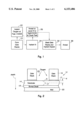
- FIG. 1 a flow chart of the present process
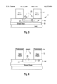
- FIG. 2 is a side view of a portion of a semiconductor device made in accordance with the present invention, during oxide implantation, schematically showing the oxide profile;
- FIG. 3 is a side view of a portion of a semiconductor device made in accordance with the present invention, after Nitrogen implantation and annealing;
- FIG. 4 is a side view of a portion of a semiconductor device made in accordance with the present invention, after source/drain dopant implantation and annealing.
- a semiconductor device 12 (FIG. 2) which includes a silicon substrate 14 having plural gate stacks 16 formed thereon in accordance with conventional principles.
- a respective gate insulator layer 17 is established between the gate stacks 16 and the substrate 14.
- the device 10 is an SOI device. Accordingly, a buried oxide layer 18 is disposed in the substrate 14, with a portion of the substrate 14 below the buried oxide layer 18 establishing a well 20.
- oxide is implanted into the substrate 14 as indicated by the arrows 23 using oxidation or Oxygen implantation principles known in the art.
- the oxide is implanted such that it establishes a concentration profile (relative to the depth dimension "depth” defined the substrate) that has a peak "P" which is spaced from the surface "S" of the substrate 14 by a distance "d” of preferably no more than five hundred Angstroms (500 ⁇ ).
- the profile of the oxide diminishes from the peak "P" until it merges with the buried oxide layer 18.
- the oxide can be implanted at an energy of thirty thousand volts (30 KeV) at a dose of up to 10 16 /cm 2 and annealed at a temperature up to 1000° C. in a furnace or using rapid thermal annealing (RTA).
- GTA rapid thermal annealing
- Nitrogen is implanted into the substrate 14, as indicated by the arrows 25 in FIG. 3, and is then annealed at block 26.
- the Nitrogen can be implanted using Nitrogen beam techniques.
- the Nitrogen is annealed, it agglomerates in the substrate 14 along the peak "P" of the oxide concentration profile to establish a boundary 27 of prospective junction regions 28.
- the boundary 27 of the prospective junction regions 28 are spaced the distance "d" from the surface "S" of the substrate 14.
- the regions 28, as shown in FIG. 3, are defined in the substrate 14 between two adjacent stacks 16.
- the implant energy of the Nitrogen and subsequent annealing are established such that the Nitrogen agglomerates along the boundary 27 at the end of the annealing process.
- the implant energy and/or annealing time and temperature is established after first determining a minimal source/drain overlap with the gate stacks 16. Some amount of junction/gate overlap is necessary for gate coupling, but the overlap should be minimized to minimize overlap capacitance. Accordingly, the Nitrogen implant energy and/or annealing is established as appropriate such that Nitrogen, after diffusing during annealing, forms a boundary of overlap regions 30. In a preferred embodiment, the distance ⁇ of overlap is no more than 400 Angstroms, and more preferably is no more than 300 Angstroms.
- the Nitrogen implant energy can be relatively low, e.g., between one thousand electron volts and ten thousand electron volts (1 KeV-10 KeV).
- the annealing can be undertaken at, e.g., seven hundred fifty degrees Celsius (750° C.) for an hour, or at 1000° C. or below for 30 seconds using rapid thermal annealing.
- the gate stacks 16 are covered with, e.g., photoresist 34 (FIG. 4), and then source/drain dopant 36 is implanted into the prospective junction regions 28 using conventional dopant implant techniques. Then, at block 38 the substrate with implanted dopant is annealed to activate the dopant. As recognized herein, the Nitrogen stops the dopant at the boundary 27 after annealing, thereby limiting the depth of the junction regions and size of the overlap regions of the device 10 and, hence, the junction and overlap capacitances.
Abstract
Description
Claims (16)
Priority Applications (1)
| Application Number | Priority Date | Filing Date | Title |
|---|---|---|---|
| US09/479,504 US6153486A (en) | 1999-12-07 | 2000-01-07 | Method for establishing shallow junction in semiconductor device to minimize junction capacitance |
Applications Claiming Priority (2)
| Application Number | Priority Date | Filing Date | Title |
|---|---|---|---|
| US16969399P | 1999-12-07 | 1999-12-07 | |
| US09/479,504 US6153486A (en) | 1999-12-07 | 2000-01-07 | Method for establishing shallow junction in semiconductor device to minimize junction capacitance |
Publications (1)
| Publication Number | Publication Date |
|---|---|
| US6153486A true US6153486A (en) | 2000-11-28 |
Family
ID=26865287
Family Applications (1)
| Application Number | Title | Priority Date | Filing Date |
|---|---|---|---|
| US09/479,504 Expired - Lifetime US6153486A (en) | 1999-12-07 | 2000-01-07 | Method for establishing shallow junction in semiconductor device to minimize junction capacitance |
Country Status (1)
| Country | Link |
|---|---|
| US (1) | US6153486A (en) |
Cited By (4)
| Publication number | Priority date | Publication date | Assignee | Title |
|---|---|---|---|---|
| US6432787B1 (en) * | 1999-06-04 | 2002-08-13 | International Business Machines Corporation | Method and apparatus for providing low-GIDL dual workfunction gate doping with borderless diffusion contact |
| US6475868B1 (en) * | 1999-08-18 | 2002-11-05 | Advanced Micro Devices, Inc. | Oxygen implantation for reduction of junction capacitance in MOS transistors |
| KR100490293B1 (en) * | 2000-12-08 | 2005-05-17 | 주식회사 하이닉스반도체 | Method of manufacturing a flash memory cell |
| US20080316828A1 (en) * | 2007-06-21 | 2008-12-25 | Hanafi Hussein I | Memory in logic cell |
Citations (3)
| Publication number | Priority date | Publication date | Assignee | Title |
|---|---|---|---|---|
| US5514902A (en) * | 1993-09-16 | 1996-05-07 | Mitsubishi Denki Kabushiki Kaisha | Semiconductor device having MOS transistor |
| US5674760A (en) * | 1996-02-26 | 1997-10-07 | United Microelectronics Corporation | Method of forming isolation regions in a MOS transistor device |
| US5908313A (en) * | 1996-12-31 | 1999-06-01 | Intel Corporation | Method of forming a transistor |
-
2000
- 2000-01-07 US US09/479,504 patent/US6153486A/en not_active Expired - Lifetime
Patent Citations (3)
| Publication number | Priority date | Publication date | Assignee | Title |
|---|---|---|---|---|
| US5514902A (en) * | 1993-09-16 | 1996-05-07 | Mitsubishi Denki Kabushiki Kaisha | Semiconductor device having MOS transistor |
| US5674760A (en) * | 1996-02-26 | 1997-10-07 | United Microelectronics Corporation | Method of forming isolation regions in a MOS transistor device |
| US5908313A (en) * | 1996-12-31 | 1999-06-01 | Intel Corporation | Method of forming a transistor |
Cited By (6)
| Publication number | Priority date | Publication date | Assignee | Title |
|---|---|---|---|---|
| US6432787B1 (en) * | 1999-06-04 | 2002-08-13 | International Business Machines Corporation | Method and apparatus for providing low-GIDL dual workfunction gate doping with borderless diffusion contact |
| US6475868B1 (en) * | 1999-08-18 | 2002-11-05 | Advanced Micro Devices, Inc. | Oxygen implantation for reduction of junction capacitance in MOS transistors |
| KR100490293B1 (en) * | 2000-12-08 | 2005-05-17 | 주식회사 하이닉스반도체 | Method of manufacturing a flash memory cell |
| US20080316828A1 (en) * | 2007-06-21 | 2008-12-25 | Hanafi Hussein I | Memory in logic cell |
| US7633801B2 (en) | 2007-06-21 | 2009-12-15 | Micron Technology, Inc. | Memory in logic cell |
| US20100055871A1 (en) * | 2007-06-21 | 2010-03-04 | Micron Technology, Inc. | Memory in logic cell |
Similar Documents
| Publication | Publication Date | Title |
|---|---|---|
| US6214654B1 (en) | Method for forming super-steep retrograded channel (SSRC) for CMOS transistor using rapid laser annealing to reduce thermal budget | |
| JP3944367B2 (en) | Method for forming insulating film and method for manufacturing semiconductor device | |
| US6873030B2 (en) | Metal gate electrode using silicidation and method of formation thereof | |
| US5963803A (en) | Method of making N-channel and P-channel IGFETs with different gate thicknesses and spacer widths | |
| US6165849A (en) | Method of manufacturing mosfet with differential gate oxide thickness on the same IC chip | |
| US6448613B1 (en) | Fabrication of a field effect transistor with minimized parasitic Miller capacitance | |
| US6291302B1 (en) | Selective laser anneal process using highly reflective aluminum mask | |
| TWI279000B (en) | Reduction of negative bias temperature instability in narrow width PMOS using F2 implantation | |
| US6468888B1 (en) | Method for forming polysilicon-germanium gate in CMOS transistor and device made thereby | |
| US4895520A (en) | Method of fabricating a submicron silicon gate MOSFETg21 which has a self-aligned threshold implant | |
| US5885887A (en) | Method of making an igfet with selectively doped multilevel polysilicon gate | |
| US6229184B1 (en) | Semiconductor device with a modulated gate oxide thickness | |
| US5677213A (en) | Method for forming a semiconductor device having a shallow junction and a low sheet resistance | |
| US6051459A (en) | Method of making N-channel and P-channel IGFETs using selective doping and activation for the N-channel gate | |
| KR100397370B1 (en) | Method for fabricating a integrated circuit having a shallow junction | |
| US6593637B1 (en) | Method for establishing component isolation regions in SOI semiconductor device | |
| US6362062B1 (en) | Disposable sidewall spacer process for integrated circuits | |
| US6313505B2 (en) | Method for forming shallow source/drain extension for MOS transistor | |
| US6153486A (en) | Method for establishing shallow junction in semiconductor device to minimize junction capacitance | |
| US6767794B2 (en) | Method of making ultra thin oxide formation using selective etchback technique integrated with thin nitride layer for high performance MOSFET | |
| KR0139773B1 (en) | Semiconductor integrated circuit device and method of manufacturing the same | |
| US6524919B2 (en) | Method for manufacturing a metal oxide semiconductor with a sharp corner spacer | |
| US6410393B1 (en) | Semiconductor device with asymmetric channel dopant profile | |
| US6204157B1 (en) | Method for establishing shallow junction in semiconductor device to minimize junction capacitance | |
| US6165877A (en) | Method for establishing shallow junction in semiconductor device to minimize junction capacitance |
Legal Events
| Date | Code | Title | Description |
|---|---|---|---|
| AS | Assignment |
Owner name: ADVANCED MICRO DEVICES, CALIFORNIA Free format text: ASSIGNMENT OF ASSIGNORS INTEREST;ASSIGNOR:IBOK, EFFIONG;REEL/FRAME:010535/0969 Effective date: 19991207 |
|
| STCF | Information on status: patent grant |
Free format text: PATENTED CASE |
|
| FPAY | Fee payment |
Year of fee payment: 4 |
|
| FPAY | Fee payment |
Year of fee payment: 8 |
|
| AS | Assignment |
Owner name: GLOBALFOUNDRIES INC., CAYMAN ISLANDS Free format text: AFFIRMATION OF PATENT ASSIGNMENT;ASSIGNOR:ADVANCED MICRO DEVICES, INC.;REEL/FRAME:023119/0083 Effective date: 20090630 |
|
| FPAY | Fee payment |
Year of fee payment: 12 |
|
| AS | Assignment |
Owner name: WILMINGTON TRUST, NATIONAL ASSOCIATION, DELAWARE Free format text: SECURITY AGREEMENT;ASSIGNOR:GLOBALFOUNDRIES INC.;REEL/FRAME:049490/0001 Effective date: 20181127 |
|
| AS | Assignment |
Owner name: GLOBALFOUNDRIES INC., CAYMAN ISLANDS Free format text: RELEASE BY SECURED PARTY;ASSIGNOR:WILMINGTON TRUST, NATIONAL ASSOCIATION;REEL/FRAME:054636/0001 Effective date: 20201117 |
|
| AS | Assignment |
Owner name: GLOBALFOUNDRIES U.S. INC., NEW YORK Free format text: RELEASE BY SECURED PARTY;ASSIGNOR:WILMINGTON TRUST, NATIONAL ASSOCIATION;REEL/FRAME:056987/0001 Effective date: 20201117 |