US6150687A - Memory cell having a vertical transistor with buried source/drain and dual gates - Google Patents
Memory cell having a vertical transistor with buried source/drain and dual gates Download PDFInfo
- Publication number
- US6150687A US6150687A US08/889,462 US88946297A US6150687A US 6150687 A US6150687 A US 6150687A US 88946297 A US88946297 A US 88946297A US 6150687 A US6150687 A US 6150687A
- Authority
- US
- United States
- Prior art keywords
- word line
- source
- bit lines
- pillar
- semiconductor
- Prior art date
- Legal status (The legal status is an assumption and is not a legal conclusion. Google has not performed a legal analysis and makes no representation as to the accuracy of the status listed.)
- Expired - Lifetime
Links
Images
Classifications
-
- H—ELECTRICITY
- H10—SEMICONDUCTOR DEVICES; ELECTRIC SOLID-STATE DEVICES NOT OTHERWISE PROVIDED FOR
- H10B—ELECTRONIC MEMORY DEVICES
- H10B12/00—Dynamic random access memory [DRAM] devices
- H10B12/01—Manufacture or treatment
- H10B12/02—Manufacture or treatment for one transistor one-capacitor [1T-1C] memory cells
- H10B12/05—Making the transistor
- H10B12/053—Making the transistor the transistor being at least partially in a trench in the substrate
-
- H—ELECTRICITY
- H10—SEMICONDUCTOR DEVICES; ELECTRIC SOLID-STATE DEVICES NOT OTHERWISE PROVIDED FOR
- H10B—ELECTRONIC MEMORY DEVICES
- H10B12/00—Dynamic random access memory [DRAM] devices
- H10B12/30—DRAM devices comprising one-transistor - one-capacitor [1T-1C] memory cells
- H10B12/48—Data lines or contacts therefor
- H10B12/488—Word lines
Definitions
- the present invention relates generally to integrated circuits, and particularly, but not by way of limitation, to a dynamic random access memory (DRAM) having a memory cell with a vertical access transistor with buried dual gates, and having buried bit and word lines.
- DRAM dynamic random access memory
- DRAMs dynamic random access memories
- a DRAM memory cell typically includes an access field-effect transistor (FET) and a storage capacitor.
- FET access field-effect transistor
- the access FET allows the transfer of data charges to and from the storage capacitor during reading and writing operations.
- the data charges on the storage capacitor are periodically refreshed during a refresh operation.
- Memory density is typically limited by a minimum lithographic feature size (F) that is imposed by lithographic processes used during fabrication.
- F lithographic feature size
- DRAMs dynamic random access memories
- Increasing the data storage capacity of semiconductor memories requires a reduction in the size of the access FET and storage capacitor of each memory cell.
- other factors such as subthreshold leakage currents and alpha-particle induced soft errors, require that larger storage capacitors be used.
- the present invention provides an integrated circuit including a pillar of semiconductor material that extends outwardly from a working surface of a substrate.
- the pillar has a number of sides.
- a transistor is formed having a body region and first and second source/drain regions within the pillar.
- the transistor includes first and second gates that are each associated with a side of the pillar.
- the invention also provides a memory device including an array of memory cells.
- Each cell includes a transistor.
- Each transistor includes a semiconductor pillar forming body and first and second source/drain regions.
- the transistor also includes first and second gates disposed adjacent to opposing sides of the pillar.
- the memory device also includes a plurality of substantially parallel first word lines. Each first word line is disposed orthogonally to the bit lines in a trench between columns of the memory cells. Each first word line allows addressing of first gates of the transistors of the memory cells that are adjacent to the trench in which the first word line is disposed.
- the memory device also includes a plurality of substantially parallel second word lines. The second word lines are interdigitated with the first word lines.
- Each second word line is disposed orthogonally to the bit lines in a trench between columns of the memory cells. Each second word line allows addressing of second gates of the transistors of the memory cells that are adjacent to the trench in which the second word line is disposed.
- a plurality of bit lines is provided, proximal to the substrate. The bit lines interconnect ones of the first source/drain regions of ones of the memory cells.
- the pillars extend outwardly from an insulating portion of the substrate. In another embodiment, the pillars extend outwardly from a semiconductor portion of the substrate.
- the invention also provides a method of fabricating an integrated circuit.
- a substrate is provided, and a plurality of bit lines are formed on the substrate.
- a plurality of access transistors are formed on each of the bit lines.
- Each access transistor includes a first source/drain region shared by at least a portion of the bit line.
- Each access transistor also includes a body region and second source/drain region formed vertically on the first source/drain region.
- a plurality of isolation trenches are formed in the substrate, orthogonal to the bit lines. Each trench is located between access transistors on the orthogonal bit lines.
- a first word line is formed in a first one of the trenches.
- the first word line controls conduction between first and second source/drain regions of access transistors that are adjacent to a first side of the first trench.
- a second word line is formed in a second one of the trenches. The second word line controls conduction between first and second source/drain regions of access transistors that are adjacent to a first side of the second trench.
- the first word line also controls conduction between first and second source/drain regions of access transistors that are adjacent to a second side of the first trench.
- the second word line also controls conduction between first and second source/drain regions of access transistors that are adjacent to a second side of the second trench.
- first word line is formed in the first trench, for controlling conduction between first and second source/drain regions of access transistors that are adjacent to a second side of the first trench.
- a second word line is formed in the second trench, for controlling conduction between first and second source/drain regions of access transistors that are adjacent to a second side of the second trench.
- the invention provides high density integrated circuit structures and fabrication methods, such as for DRAM memory cell arrays and other semiconductor devices.
- Each memory cell can be fabricated in a surface area that is approximately 4F 2 , where F is a minimum lithographic feature size.
- F is a minimum lithographic feature size.
- a common first word line is shared by all of the access FETs that are located along both sides of the trench in which the first word line is located.
- a common second word line is shared by all of the access FETs that are located along both sides of the trench in which the second word line is located.
- split word lines are provided in either or both trenches. The split word lines provide separate addressing of gate regions of access FETs on opposite sides of the trench.
- Each of the unitary and split word line embodiments can be fabricated on a bulk semiconductor substrate, or on a semiconductor-on-insulator (SOI) substrate that results from using an SOI starting material, or by forming SOI regions during fabrication.
- SOI embodiments provide greater immunity to alpha-particle induced soft errors, allowing the use of smaller storage capacitors.
- FIG. 1 is a schematic representation illustrating generally one embodiment of a semiconductor memory according to the invention.
- FIG. 2 is a perspective view illustrating generally one embodiment of a portion of a memory according to the present invention.
- FIG. 3 is a plan view illustrating generally memory cells according to one embodiment of the invention as viewed from above the structures formed on the substrate.
- FIG. 4 is a cross-sectional view taken along the cut line 4--4 of FIG. 3.
- FIGS. 5A-K describe generally various processing techniques of one embodiment of a method of fabricating memory cells according to the invention.
- FIG. 6 is a perspective view illustrating generally another embodiment of a portion of a memory according to the present invention having a semiconductor-on-insulator (SOI) substrate.
- SOI semiconductor-on-insulator
- FIGS. 7A-C illustrate generally, by way of example, additional steps used to form SOI bars according to one embodiment of the invention.
- FIG. 8 is a perspective view illustrating generally another embodiment of a portion of a memory according to the present invention in which split gates are formed.
- FIG. 9 is a plan view illustrating generally memory cells according to a split gate embodiment of the invention as viewed from above the structures formed on the substrate.
- FIG. 10 is a cross-sectional view taken along the cut line 10--10 of FIG. 9.
- FIG. 11 is a perspective view illustrating generally another embodiment of a portion of a memory according to the present invention including split gates and a bulk semiconductor substrate.
- FIG. 12 is a cross-sectional view taken along the cut line 12--12 of FIG. 11.
- wafer and substrate are interchangeably used to refer generally to any structure on which integrated circuits are formed, and also to such structures during various stages of integrated circuit fabrication. Both terms include doped and undoped semiconductors, epitaxial layers of a semiconductor on a supporting semiconductor or insulating material, combinations of such layers, as well as other such structures that are known in the art.
- doped and undoped semiconductors include doped and undoped semiconductors, epitaxial layers of a semiconductor on a supporting semiconductor or insulating material, combinations of such layers, as well as other such structures that are known in the art.
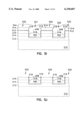
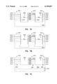
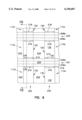
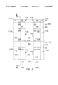
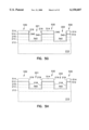
- FIG. 1 is a schematic representation illustrating generally one embodiment of an integrated circuit 100, such as a semiconductor memory device, incorporating an array of memory cells provided by the invention.
- circuit 100 illustrates, by way of example but not by way of limitation, a dynamic random access memory (DRAM), but the invention also comprises other integrated circuits including any other semiconductor memory devices.
- circuit 100 includes memory cell arrays 110, such as 110A and 110B. Each array 110 includes M rows and N columns of memory cells 112.
- each memory cell includes a transfer device, such as n-channel cell access field-effect transistor (FET) 130 or any other transistor or switching device having more than one control terminal inputs. More particularly, access FET 130 includes first and second gate terminals for controlling conduction between its first and second source/drain terminals.
- FET field-effect transistor
- Access FET 130 is coupled at a second source/drain terminal to a storage node of a storage capacitor 132.
- the other terminal of storage capacitor 132 is coupled to a reference voltage such as a ground voltage VSS.
- Each of the M rows includes one of word lines WL0, WL1 . . . WLm-1, WLm coupled to the first gate terminals of access FETs 130 or to one of the control terminals of an equivalent switching device.
- Each of the M rows also includes one of word lines R1, R2, . . . , Rm-1, Rm coupled to the second gate terminals of access FETs 130 in memory cells 112.
- word line includes any interconnection line between gate terminals of access FETs 130, or the control terminals of equivalent switching devices.
- Each of the N columns includes one of bit lines BL0, BL1 . . . BLn-1, BLn.
- Bit lines BL0-BLN are used to write to and read data from memory cells 112.
- Word lines WL0-WLm and R1-Rm are used to activate access FETs 130 to access a particular row of memory cells 112 that is to be written or read.
- Addressing circuitry is also included.
- address buffer 114 controls column decoders 118, which also include sense amplifiers and input/output circuitry that is coupled to bit lines BL0-BLn.
- Address buffer 114 also controls row decoders 116.
- Row decoders 116 and column decoders 118 selectably access memory cells 112 in response to address signals that are provided on address lines 120 during read and write operations.
- the address signals are typically provided by an external controller such as a microprocessor or other memory controller.
- Each of memory cells 112 has a substantially identical structure, and accordingly, only one memory cell 112 structure is described herein.
- circuit 100 receives an address of a particular memory cell 112 at address buffer 114.
- Address buffer 114 identifies one of the word lines WL0-WLm of the particular memory cell 112 to row decoder 116.
- Row decoder 116 selectively activates the particular word line WL0-WLm to activate access FETs 130 of each memory cell 112 that is connected to the selected word line WL0-WLm.
- Column decoder 118 selects the one of bit lines BL0-BLn of the particularly addressed memory cell 112.
- data received by input/output circuitry is coupled to the one of bit lines BL0-BLn and through the access FET 130 to charge or discharge the storage capacitor 132 of the selected memory cell 112 to represent binary data.
- data stored in the selected memory cell 112, as represented by the charge on its storage capacitor 132 is coupled to the one of bit lines BL0-BLn, amplified, and a corresponding voltage level is provided to the input/output circuits.
- each of the first and second gates of access FET 130 is capable of controlling the conduction between its first and second source/drain terminals, as described below.
- parallel switching functionality can be effected between the first and second source/drain terminals of access FET 130 by independently operating the particular ones of word lines WL0-WLm and corresponding ones of word lines R0-Rm. For example, by independently activating word line WL0 and word line R0, both of which are coupled to the same row of memory cells 112, independently controlled inversion channels can be formed in each corresponding access FET 130 by respective first and second gates for allowing conduction between the first and second source/drain regions.
- each of the first and second gates of access FET 130 is capable of controlling the conduction between its first and second source/drain terminals, but the first and second gates of particular access FETs 130 are synchronously activated, rather than independently operated.
- first and second gates of particular access FETs 130 are synchronously activated, rather than independently operated.
- word line WL0 and word line R0 both of which are coupled to the same row of memory cells 112
- synchronously activated inversion channels can be formed in each corresponding access FET 130 by respective first and second gates for allowing conduction between the first and second source/drain regions.
- synchronous activation and deactivation of the first and second gates allows better control over the potential distributions in the access FET 130 when it is in a conductive state. Synchronous activation and deactivation can be used to obtain well-controlled fully depleted operating characteristics of access FET 130.
- different activation voltages can be applied to the first and second gates of the access FET 130.
- different voltages can be provided to synchronously activated word lines WL0 and R0, thereby providing different activation voltages to the first and second gates of the access FET 130 to obtain particular desired operating characteristics.
- different deactivation voltages can be applied to the first and second gates of the access FET 130.
- different deactivation voltages can be provided to synchronously deactivated word lines WL0 and R0 and corresponding first and second gates of access FETs 130, in order to obtain particular desired operating characteristics.
- different activation and deactivation voltages can be applied to independently operated word lines such as WL0 and R0.
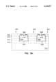
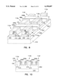
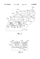
- FIG. 2 is a perspective view illustrating generally one embodiment of a portion of a memory according to the present invention.
- FIG. 2 illustrates portions of six memory cells 112a-f, including portions of vertically oriented access FETs 130 therein.
- Conductive segments of bit lines 202 represent particular ones of bit lines BL0-BLn.
- Conductive segments of first word line 206 represents any one of word lines WL0-WLm, which provide integrally formed first gates for access FETs 130 between which the particular first word line 206 is interposed.
- Conductive segments of second word line 208 represents any one of word lines R0-Rm, which provide integrally formed second gates for access FETs 130 between which the particular second word line 208 is interposed.
- word lines WL0-WLm and R0-Rm are alternatingly disposed (interdigitated) within the array 110.
- the detailed description of memory cell 112 structure refers only to memory cells 112a-f, bit lines 202, and respective first and second word lines 206 and 208 that are associated with memory cells 112a-f. However, the following description similarly applies to all memory cells 112 and similar conductive lines in array 110.
- vertically oriented access FETs 130 are formed in semiconductor pillars that extend outwardly from an underlying substrate 210.
- substrate 210 includes bulk semiconductor starting material, semiconductor-on-insulator (SOI) starting material, or SOI material that is formed from a bulk semiconductor starting material during processing.
- SOI semiconductor-on-insulator
- access FETs 130 include an n+ silicon layer formed on a bulk silicon substrate 210 to produce first source/drain regions 212 of access FETs 130 and integrally formed n++ conductively doped bit lines 202 defining a particular column of memory cells 112.
- a p- silicon layer is formed on n+ first source/drain region 212 to form the body region 214 of access FET 130, in which inversion channels may be capacitively generated at the sidewalls of the semiconductor pillar under the control of the first and second gates.
- a further n+ silicon layer is formed on p- body region 214 to produce second source/drain region 216 of access FET 130.
- Storage capacitors 132 are formed on the second/source drain regions 216.
- Word lines WL0-WLm and R0-Rm are altematingly disposed (interdigitated) within the array 110.
- first word line 206 is interposed between semiconductor pillars of memory cell pairs 112a-b and 112d-e.
- Second word line 208 is interposed between semiconductor pillars of memory cell pairs 112b-c and 112e-f.
- access FETs 130 are formed on bit lines 202 in semiconductor pillars extending outwardly from substrate 210 and including body regions 214, and first and second source drain regions 212 and 216, respectively.
- bit lines 202 contact bulk semiconductor substrate 210.
- Isolation trenches provide isolation between access FETs 130 of adjacent memory cells 112. Columns of memory cells 112 are separated by a trench 220 that is subsequently filled with a suitable insulating material such as silicon dioxide. For example, trench 220 provides isolation between memory cells 112a and 112d and between memory cells 112b and 112e. Rows of memory cells 112 are alternatingly separated by a trench 221 and 222, each of which are separated from substrate 210 by an underlying insulating layer, described below, and separated from the body region 214 of access FETs 130 by a gate oxide, also described below. For example, trench 221 provides isolation between memory cells 112a and 112b and between memory cells 112d and 112e. In addition, trench 222 provides isolation between memory cells 112b and 112c and memory cells 112e and 112f. Trenches 221 and 222 extend substantially orthogonally to bit lines 202.
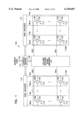
- FIG. 3 is a plan view illustrating generally memory cells 112a-f as viewed from above the structures formed on substrate 210.
- FIG. 3 illustrates subsequently formed insulator such as oxide 224, formed in trenches 220 to provide isolation between memory cells 112.
- first word line 206 is shared between first gates of access FETs 130 of memory cells 112 in adjacent rows, such as between memory cells 112a-b and 112d-e.
- First word line 206 is also shared between first gates of other access FETs 130 that are in the same adjacent rows, but coupled to different bit lines 202.
- First word line 206 is located in trench 221 that extends between the semiconductor pillars of memory cells 112a and 112b.
- First word line 206 is separated by gate oxide 218 from the vertical sidewalls 219 of the semiconductor pillars on each side of trench 221.
- Second word line 208 is shared between second gates of access FETs 130 of memory cells 112 in adjacent rows, such as between memory cells 112b-c and 112e-f. Second word line 208 is also shared between second gates of other access FETs 130 that are in the same adjacent rows, but coupled to different bit lines 202. Second word line 208 is located in trench 222 that extends between the semiconductor pillars of memory cells 112b and 112c. Second word line 208 is separated by gate oxide 218 from the vertical sidewalls 223 of the semiconductor pillars on each side of trench 222.
- FIG. 4 is a cross-sectional view taken along the cut line 4--4 of FIG. 3.
- respective first and second word lines 206 and 208 are buried below the active semiconductor surface 230 of the semiconductor pillar in the memory cells 112. Active semiconductor surface 230 represents an upper semiconductor portion of second source/drain region 216.
- First and second word lines 206 and 208 are isolated from adjacent semiconductor pillars by gate oxide 218.
- First and second word lines 206 and 208 respectively provide integrally formed first and second gate portions that are capacitively coupled to adjacent access FET 130 body regions 214, such as for forming inversion channel regions therein.
- respective first and second word lines 206 and 208 are formed of a refractory metal, such as tungsten or titanium.
- first and second word lines 206 and 208 can be formed of n+ doped polysilicon.
- other suitable conductors could also be used for first and second words lines 206 and 208, respectively.
- Burying first and second word lines 206 and 208 below semiconductor surface 230 provides additional space on the upper portion of memory cell 112 for formation of storage capacitors 132. Increasing the area available for forming storage capacitor 132 increases the possible obtainable capacitance value of storage capacitor 132.
- storage capacitor 132 is a stacked capacitor that is formed using any of the many capacitor structures and process sequences known in the art. Other techniques could also be used for implementing storage capacitor 132. Contacts to the first and second word lines 206 and 208, respectively, can be made outside of the memory array 110.
- respective first and second word lines 206 and 208 are shared between adjacent memory cells 112. As a result, only one-half the surface line width of each is allocated to each memory cell.
- the row pitch of each cell measured from the centerline of first word line 206 to the centerline of second word line 208, can be approximately 2F, where F is a minimum lithographic feature size. F corresponds to the length and width presented by the surface of a minimum-sized semiconductor pillar in each memory cell 112.
- the column pitch of each cell, measured between centerlines of bit lines 202 can be approximately 2F.
- the surface area of each memory cell 112 can be approximately 4F 2 .
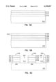
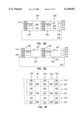
- FIGS. 5A-K describe generally various processing techniques of one embodiment of a method of fabricating memory cells 112, such as shown in FIGS. 2-4, using bulk silicon processing techniques.
- a p-bulk silicon substrate 210 starting material is used.
- An n++ and n+ silicon composite first source/drain layer 212 is formed on substrate 210, such as by ion-implantation, epitaxial growth, or a combination of such techniques.
- the more heavily conductively doped lower portion of the first/source drain layer 212 also functions as the bit line 202.
- the thickness of the n++ portion of first source/drain layer 212 is that of the desired bit line 202 thickness, which can be approximately between 0.1 to 0.25 ⁇ m.
- the overall thickness of the first source/drain layer 212 can be approximately between 0.2 to 0.5 ⁇ m.
- a body region layer 214 of p- silicon is formed, such as by epitaxial growth, to a thickness that can be about 0.4 ⁇ m.
- a second source/drain region layer 216 of n+ silicon is formed, such as by ion-implantation into body region layer 214 or by epitaxial growth on body region layer 214, to a thickness that can be approximately between 0.2 and 0.5 ⁇ m.
- an SiO 2 thin pad oxide layer 512 is formed on second source/drain region 216, such as by chemical vapor deposition (CVD).
- pad oxide layer 512 can be approximately 10 nm in thickness.
- a thin silicon nitride (Si 3 N 4 ) layer 514 is formed on pad oxide layer 512, such as by CVD.
- nitride layer 514 of can be approximately 100 nm in thickness.
- photoresist is applied and selectively exposed to provide a mask for the directional etching of trenches 220, such as by reactive ion etching (RIE).
- RIE reactive ion etching
- the directional etching results in a plurality of column bars 516 containing the stack of nitride layer 514, pad oxide layer 512, second source/drain layer 216, body region layer 214, and first source/drain layer 212.
- Trenches 220 are etched to a depth that is sufficient to reach the surface 518 of substrate 210, thereby providing separation between conductively doped bit lines 202.
- Bars 516 are oriented in the direction of bit lines 202. In one embodiment, bars 516 have a surface line width of approximately one micron or less. The depth and width of each trench 220 can be approximately equal to the line width of bars 516.
- Isolation material 224 such as SiO 2 is deposited to fill the trenches 220.
- the working surface is then planarized, such as by chemical mechanical polishing/planarization (CMP).
- FIG. 5E illustrates the view of FIG. 5D after clockwise rotation by ninety degrees.
- a photoresist material is applied and selectively exposed to provide a mask for the directional etching of trenches 221 and 222, such as by reactive ion etching (RIE) of a plurality of row bars 532 that are disposed orthogonally to bit lines 202.
- RIE reactive ion etching
- Forming trenches 221 and 222 includes etching though stacked layers in the portions of bars 516.
- Forming trenches 221 and 222 also includes etching through the isolation material 224 disposed between bars 516.
- trenches 221 and 222 are etched through nitride layer 514, pad oxide layer 512, second source/drain layer 216, body region layer 214, and partially into first source/drain layer 212.
- Trenches 221 and 222 are etched into bars 516 to a depth of about 100 nm into first source/drain layer 212, leaving intact an underlying bit line 202 portion of the first source/drain layer 212.
- Trenches 221 and 222 are also etched into the isolation material 224 between bars 516.
- a nonselective dry etch is used to remove the isolation material 224 between bars 516 and also the pad oxide layer 512, second source/drain layer 216, body region layer 214, and a portion of first source/drain layer 212 of bars 516.
- the directional etching of trenches 221 and 222 results in the formation of a plurality of row bars 532 that are orthogonal to column bars 516.
- FIG. 5F is a plan view illustrating generally the arrangement of parallel bars 516, and trenches 220 interposed therebetween. Bars 532 are arranged orthogonally to bars 516. Trenches 221 and 222 are interposed between ones of bars 532. The resulting semiconductor pillars in the intersecting portions of bars 532 and 516 provide first and second source drain regions 212 and 216, respectively, and body region 214 for access FETs 130 of memory cells 112.
- a conformal silicon nitride layer 540 is formed, such as by CVD.
- Nitride layer 540 is directionally etched, such as by RIE, to leave resulting portions of nitride layer 540 only on sidewalls 219 of the bars 532 in trenches 221 and 222.
- the thickness of nitride layer 540 is about 20 nm.
- An oxide layer 542 is formed, such as by thermal growth, at the base portions of trenches 221 and 222. Oxide layer 542 insulates the underlying bit lines 202 from structures subsequently formed in trenches 221 and 222. After forming oxide layer 542, remaining portions of nitride layer 540 are removed.
- a gate oxide 218 is formed on the exposed sidewalls 219 portions in trenches 221 and 222 of second source/drain region 216, body region 214, and first source/drain region 212.
- gate oxide 218 is a high-quality thin oxide layer that is thermally grown on the exposed sidewalls 219 of trenches 221 and 222.
- a conductive layer 544 is formed over the working surface of the wafer, including filling trenches 221 and 222 in which respective first and second word lines 206 and 208 will be formed.
- layer 544 is formed by CVD of a refractory metal, such as tungsten.
- layer 544 is formed by CVD of n+ polysilicon.
- first and second word lines 206 and 208 are formed in respective trenches 221 and 222.
- FIG. 5K illustrates one embodiment in which, an insulating layer 546, such as SiO 2 , is formed on the working surface of the wafer, such as by CVD.
- the structure thus formed is then processed to fabricate a storage capacitor 132 on the working surface of the wafer, using known techniques, followed by conventional back end of line (BEOL) procedures.
- BEOL back end of line
- FIG. 6 is a perspective view illustrating generally another embodiment of a portion of a memory according to the present invention, similar to that described with respect to FIG. 2.
- SOI substrate 210 of FIG. 6 is obtained using an SOI starting material.
- a bulk semiconductor starting material is used, and an bars of SOI are formed during fabrication of circuit 100, such that the semiconductor pillars, in which portions of access FETs 130 are formed, extend outwardly from an insulating portion 602 of substrate 210.
- FIGS. 7A-C illustrate generally, by way of example, additional steps used to form SOI bars during the fabrication steps described above with respect to FIGS. 5A-K, such that the semiconductor pillars, in which portions of access FETs 130 are formed, extend outwardly from an insulating portion 602 of substrate 210, resulting in the structure illustrated in FIG. 6.
- FIG. 7A the processing steps described above with respect to FIGS. 5A-C are carried out, forming trenches 220 that are etched to a depth that is below the original surface 518 of substrate 210, such as by approximately greater than or equal to 0.6 ⁇ m.
- a nitride layer 704 is formed, such as by CVD.
- Nitride layer 704 is directionally etched, such as by RIE, to remove nitride layer 704 from the base regions of trenches 220. Portions of nitride layer 704 remain on the sidewall of trenches 220 to protect adjacent layers during subsequent etching and oxidation.
- an isotropic chemical etch of silicon is used to partially undercut bars 516.
- hydrofluoric acid (HF) or a commercial etchant sold under the trade name CP4 a mixture of approximately 1 part (46% HF):1 part (CH 3 COOH):3 parts (HNO 3 )
- CP4 a mixture of approximately 1 part (46% HF):1 part (CH 3 COOH):3 parts (HNO 3 )
- the partial undercutting of bars 516 by isotropic etching is timed to remove a volume of silicon that is sufficient to compensate for a subsequently formed volume of oxide, described below.
- the subsequent oxidation step produces a volume of oxide that is approximately twice that of the silicon consumed during oxidation.
- substrate 210 is oxidized using a standard semiconductor processing furnace at a temperature of approximately 900 to 1,100 degrees Celsius.
- a wet oxidizing ambient is used in the furnace chamber to oxidize the exposed silicon regions in the lower portion of trenches 220.
- Substrate 210 is oxidized for a time period that is sufficient to form oxide insulating portion 602 that fully undercuts bars 516. Insulating portion 602 underlies both bars 516 and trenches 220, and isolates the bit lines 202 and access FETs 130 formed on bit lines 202 from an underlying semiconductor portion of substrate 210.
- Nitride layer 704 is removed, and processing then continues as described above with respect to FIGS. 5D-K, resulting in the structure of FIG. 6.
- bars 516 are sufficiently narrow such that the oxidation step that undercuts bars 516 produces sufficient oxide to fill trenches 220, resulting in a generally planar structure. This avoids the need for a separate step of depositing an oxide insulation material 224 described with respect to FIG. 5D.
- the oxidation time period depends on the width of bars 516 and the effective width of bars 516 after the undercut etch step. Narrower bars 516 require shorter oxidation times. For example, for sub-0.25 micron technology, oxidation time is approximately 1 hour. In another embodiment, the etch step fully undercuts bars 516 before oxidation. This further reduces oxidation time.
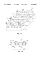
- FIGS. 8-10 illustrate generally another embodiment of a portion of a memory according to the present invention, similar to that described with respect to FIG. 6.
- first and second word lines 206 and 208 are each split into separate conductors.
- First word line 206 is split into independently operable first word lines 206a and 206b, each disposed in trench 221 and electrically isolated from each other.
- Second word line 208 is split into independently operable second word lines 208a and 208b, each disposed in trench 222 and electrically isolated from each other, such as by SiO 2 .
- gate regions need not be shared between access FETs 130 in adjacent memory cells 112 on opposing sides of trenches 221 and 222.
- First and second word lines 206 and 208 can be formed of a refractory metal or n+ polysilicon or other suitable conductor, as described above.
- first word line 206a extends in trench 221 adjacent to the vertical sidewalls 219 of the semiconductor pillars of in-line memory cells 112a and 112d, separated therefrom by gate oxide 218.
- First word line 206b extends in trench 221 adjacent to the vertical sidewalls 219 of the semiconductor pillars of in-line memory cells 112b and 112e, separated therefrom by gate oxide 218.
- Second word line 208a extends in trench 222 adjacent to the vertical sidewalls 219 of the semiconductor pillars of in-line memory cells 112b and 112e, separated therefrom by gate oxide 218.
- Second word line 208b extends in trench 222 adjacent to the vertical sidewalls 219 of the semiconductor pillars of in-line memory cells 112c and 112f.
- Operation of the access FET 130 of memory cell 112b includes operation of the first word line 206b and second word line 208a, as described above.
- a positive potential is applied to either or both of first word line 206b and second word line 208a, as described above to turn on the access FET 130 of memory cell 112b.
- first word line 206b is not shared by the access FET 130 of memory cell 112a, subthreshold leakage is not induced in the access FET 130 of memory cell 112a during activation of first word line 206b to operate the access FET 130 of memory cell 112b.
- second word line 208a is not shared by the access FET 130 of memory cell 112c, subthreshold leakage in the access FET 130 of memory cell 112c is not induced during activation of second word line 208a to operate the access FET 130 of memory cell 112b.
- split first word lines 206a-b and split second word lines 208a-b avoids the problem of sub-threshold conduction in access FETs 130 in one row while the memory cells 112 in the adjacent row are being addressed.
- Each memory cell 112 is capable of being uniquely addressed by a combination of first word line 206 and second word line 208 voltages. These voltages need not appear on the first word line 206 and second word line 208 of adjacent rows of memory cells 112.
- FIGS. 8-10 can be fabricated by process steps similar to those described with respect to FIGS. 5A-C forming bars 516 separated by trenches 220. This is followed by the process steps described with respect to FIGS. 7A-C follow, isolating bars 516 from an underlying semiconductor portion of substrate 210 by insulating portion 602. This is followed by the process steps described with respect to FIGS. 5D-J forming a planar structure including a unitary conductor first word line 206 in first trench 221 and a unitary conductor second word line 208 in second trench 222.
- Unitary conductor first word line 206 thus formed is split to form separate conductors 206a-b.
- a refractory metal, n+ polysilicon, or other conductor is deposited as a conformal film that can have a thickness of less than or equal to approximately F/3, where F is the minimum feature size.
- the conformal film is then directionally etched, thereby leaving resulting split conductor word lines 206a-b adjacent to the vertical sidewall 219, separated therefrom by gate oxide 218.
- Second word line 208 can be similarly split into separate conductors 208a-b during the same deposition and directional etch steps.
- Splitting unitary conductor first and second word lines 206 and 208, respectively provides the resulting structures illustrated in FIGS. 8-10, but is not required to practice the invention. These steps can be omitted, such as to obtain the structures illustrated in FIGS. 2-4.
- FIGS. 11-12 illustrate generally another embodiment of a portion of a memory according to the present invention, similar to that described with respect to FIGS. 8-10, but fabricating using a bulk silicon substrate 210, as described with respect to FIGS. 2-4.
- the structures of FIGS. 11-12 are fabricated by process steps similar to those described with respect to FIGS. 5A-C, forming bars 516 separated by trenches 220.
- the process steps described with respect to FIGS. 7A-C follow are omitted from this embodiment. Instead, this is followed by the process steps described with respect to FIGS. 5D-J forming a planar structure including a unitary conductor first word line 206 in first trench 221 and a unitary conductor second word line 208 in second trench 222.
- the unitary conductor first and second word lines 206 and 208, respectively, are then split as described above with respect to FIGS. 8-10.
- DRAMs dynamic random access memories
- the scope of the invention includes any other integrated circuit applications in which the above structures and fabrication methods are used.
- Each memory cell includes a vertical access FET, formed on a bit line, and first and second gates integrally formed with respective first and second word lines that are buried in trenches that extend along opposite sides of the memory cell.
- Each memory cell can be fabricated in a surface area that is approximately 4F 2 , where F is a minimum lithographic feature size.
- a common first word line is shared by all of the access FETs that are located along both sides of the trench in which the first word line is located.
- a common second word line is shared by all of the access FETs that are located along both sides of the trench in which the second word line is located.
- split word lines are provided in each trench, and the two split word lines provide separate addressing of gate regions of access FETs on opposite sides of the trench.
- Each of the unitary and split word line embodiments can be fabricated on a bulk semiconductor substrate, or on a semiconductor-on-insulator (SOI) substrate that results from using an SOI starting material, or by forming SOI regions during fabrication.
- SOI semiconductor-on-insulator
Abstract
Description
Claims (24)
Priority Applications (5)
| Application Number | Priority Date | Filing Date | Title |
|---|---|---|---|
| US08/889,462 US6150687A (en) | 1997-07-08 | 1997-07-08 | Memory cell having a vertical transistor with buried source/drain and dual gates |
| US09/139,164 US6350635B1 (en) | 1997-07-08 | 1998-08-24 | Memory cell having a vertical transistor with buried source/drain and dual gates |
| US09/596,266 US6399979B1 (en) | 1997-07-08 | 2000-06-16 | Memory cell having a vertical transistor with buried source/drain and dual gates |
| US09/651,199 US6504201B1 (en) | 1997-07-08 | 2000-08-30 | Memory cell having a vertical transistor with buried source/drain and dual gates |
| US10/162,942 US6818937B2 (en) | 1997-07-08 | 2002-06-04 | Memory cell having a vertical transistor with buried source/drain and dual gates |
Applications Claiming Priority (1)
| Application Number | Priority Date | Filing Date | Title |
|---|---|---|---|
| US08/889,462 US6150687A (en) | 1997-07-08 | 1997-07-08 | Memory cell having a vertical transistor with buried source/drain and dual gates |
Related Child Applications (3)
| Application Number | Title | Priority Date | Filing Date |
|---|---|---|---|
| US09/139,164 Division US6350635B1 (en) | 1997-07-08 | 1998-08-24 | Memory cell having a vertical transistor with buried source/drain and dual gates |
| US09/596,266 Continuation US6399979B1 (en) | 1997-07-08 | 2000-06-16 | Memory cell having a vertical transistor with buried source/drain and dual gates |
| US09/651,199 Continuation US6504201B1 (en) | 1997-07-08 | 2000-08-30 | Memory cell having a vertical transistor with buried source/drain and dual gates |
Publications (1)
| Publication Number | Publication Date |
|---|---|
| US6150687A true US6150687A (en) | 2000-11-21 |
Family
ID=25395151
Family Applications (5)
| Application Number | Title | Priority Date | Filing Date |
|---|---|---|---|
| US08/889,462 Expired - Lifetime US6150687A (en) | 1997-07-08 | 1997-07-08 | Memory cell having a vertical transistor with buried source/drain and dual gates |
| US09/139,164 Expired - Fee Related US6350635B1 (en) | 1997-07-08 | 1998-08-24 | Memory cell having a vertical transistor with buried source/drain and dual gates |
| US09/596,266 Expired - Lifetime US6399979B1 (en) | 1997-07-08 | 2000-06-16 | Memory cell having a vertical transistor with buried source/drain and dual gates |
| US09/651,199 Expired - Lifetime US6504201B1 (en) | 1997-07-08 | 2000-08-30 | Memory cell having a vertical transistor with buried source/drain and dual gates |
| US10/162,942 Expired - Fee Related US6818937B2 (en) | 1997-07-08 | 2002-06-04 | Memory cell having a vertical transistor with buried source/drain and dual gates |
Family Applications After (4)
| Application Number | Title | Priority Date | Filing Date |
|---|---|---|---|
| US09/139,164 Expired - Fee Related US6350635B1 (en) | 1997-07-08 | 1998-08-24 | Memory cell having a vertical transistor with buried source/drain and dual gates |
| US09/596,266 Expired - Lifetime US6399979B1 (en) | 1997-07-08 | 2000-06-16 | Memory cell having a vertical transistor with buried source/drain and dual gates |
| US09/651,199 Expired - Lifetime US6504201B1 (en) | 1997-07-08 | 2000-08-30 | Memory cell having a vertical transistor with buried source/drain and dual gates |
| US10/162,942 Expired - Fee Related US6818937B2 (en) | 1997-07-08 | 2002-06-04 | Memory cell having a vertical transistor with buried source/drain and dual gates |
Country Status (1)
| Country | Link |
|---|---|
| US (5) | US6150687A (en) |
Cited By (133)
| Publication number | Priority date | Publication date | Assignee | Title |
|---|---|---|---|---|
| US20010035549A1 (en) * | 1998-01-22 | 2001-11-01 | Leonard Forbes | Circuits with a trench capacitor having micro-roughened semiconductor surfaces |
| US6359804B2 (en) * | 1998-04-16 | 2002-03-19 | Mitsubishi Denki Kabushiki Kaisha | Static semiconductor memory cell formed in an n-well and p-well |
| US6377070B1 (en) | 2001-02-09 | 2002-04-23 | Micron Technology, Inc. | In-service programmable logic arrays with ultra thin vertical body transistors |
| US6395602B2 (en) | 1996-01-03 | 2002-05-28 | Micron Technology, Inc. | Method of forming a capacitor |
| US6399979B1 (en) * | 1997-07-08 | 2002-06-04 | Micron Technology, Inc. | Memory cell having a vertical transistor with buried source/drain and dual gates |
| US6424001B1 (en) | 2001-02-09 | 2002-07-23 | Micron Technology, Inc. | Flash memory with ultra thin vertical body transistors |
| US6448601B1 (en) | 2001-02-09 | 2002-09-10 | Micron Technology, Inc. | Memory address and decode circuits with ultra thin body transistors |
| US6476434B1 (en) | 1997-07-08 | 2002-11-05 | Micron Tecnology, Inc. | 4 F2 folded bit line dram cell structure having buried bit and word lines |
| US20020164853A1 (en) * | 2000-08-22 | 2002-11-07 | Micron Technology, Inc. | Vertical gate transistors in pass transistor programmable logic arrays |
| US6486027B1 (en) | 1998-02-27 | 2002-11-26 | Micron Technology, Inc. | Field programmable logic arrays with vertical transistors |
| US6486703B2 (en) | 1998-08-04 | 2002-11-26 | Micron Technology, Inc. | Programmable logic array with vertical transistors |
| US6496034B2 (en) | 2001-02-09 | 2002-12-17 | Micron Technology, Inc. | Programmable logic arrays with ultra thin body transistors |
| US6498065B1 (en) | 1998-08-04 | 2002-12-24 | Micron Technology, Inc. | Memory address decode array with vertical transistors |
| US6531727B2 (en) | 2001-02-09 | 2003-03-11 | Micron Technology, Inc. | Open bit line DRAM with ultra thin body transistors |
| US6537871B2 (en) | 1997-10-06 | 2003-03-25 | Micron Technology, Inc. | Circuit and method for an open bit line memory cell with a vertical transistor and trench plate trench capacitor |
| US6556068B2 (en) | 1998-02-26 | 2003-04-29 | Micron Technology, Inc. | Threshold voltage compensation circuits for low voltage and low power CMOS integrated circuits |
| US6559491B2 (en) | 2001-02-09 | 2003-05-06 | Micron Technology, Inc. | Folded bit line DRAM with ultra thin body transistors |
| US6566682B2 (en) | 2001-02-09 | 2003-05-20 | Micron Technology, Inc. | Programmable memory address and decode circuits with ultra thin vertical body transistors |
| US20030113970A1 (en) * | 2001-12-14 | 2003-06-19 | Fried David M. | Implanted asymmetric doped polysilicon gate FinFET |
| US6597037B1 (en) | 1998-02-27 | 2003-07-22 | Micron Technology, Inc. | Programmable memory address decode array with vertical transistors |
| US6597203B2 (en) * | 2001-03-14 | 2003-07-22 | Micron Technology, Inc. | CMOS gate array with vertical transistors |
| US20030142564A1 (en) * | 1997-10-06 | 2003-07-31 | Micron Technology, Inc. | Circuit and method for an open bit line memory cell with a vertical transistor and trench plate trench capacitor |
| US20030151077A1 (en) * | 2002-02-13 | 2003-08-14 | Leo Mathew | Method of forming a vertical double gate semiconductor device and structure thereof |
| US20030153156A1 (en) * | 2001-02-15 | 2003-08-14 | Leonard Forbes | Logic array and dynamic logic method |
| US20030235066A1 (en) * | 2002-06-21 | 2003-12-25 | Micron Technology, Inc. | Ferroelectric write once read only memory for archival storage |
| US20030235081A1 (en) * | 2002-06-21 | 2003-12-25 | Micron Technology, Inc. | Nanocrystal write once read only memory for archival storage |
| US20030235085A1 (en) * | 2002-06-21 | 2003-12-25 | Micron Technology, Inc. | Write once read only memory employing charge trapping in insulators |
| US20040004247A1 (en) * | 2002-07-08 | 2004-01-08 | Micron Technology, Inc. | Memory utilizing oxide-nitride nanolaminates |
| US20040042256A1 (en) * | 2002-08-29 | 2004-03-04 | Micron Technology, Inc. | Single transistor vertical memory gain cell |
| US20040041236A1 (en) * | 2002-08-29 | 2004-03-04 | Micron Technology, Inc. | Merged mos-bipolar capacitor memory cell |
| US6703663B1 (en) * | 1998-02-27 | 2004-03-09 | Taiwan Semiconductor Manufacturing Company | CMOS device using additional implant regions to enhance ESD performance and device manufactured thereby |
| US6744094B2 (en) | 2001-08-24 | 2004-06-01 | Micron Technology Inc. | Floating gate transistor with horizontal gate layers stacked next to vertical body |
| US20040108532A1 (en) * | 2002-12-04 | 2004-06-10 | Micron Technology, Inc. | Embedded DRAM gain memory cell |
| US6750487B2 (en) | 2002-04-11 | 2004-06-15 | International Business Machines Corporation | Dual double gate transistor |
| US6764901B2 (en) | 1997-10-06 | 2004-07-20 | Micron Technology, Inc. | Circuit and method for a folded bit line memory cell with vertical transistor and trench capacitor |
| US6777744B2 (en) | 1998-02-24 | 2004-08-17 | Micron Technology, Inc. | Circuits and methods using vertical, complementary transistors |
| US6804142B2 (en) | 2002-11-12 | 2004-10-12 | Micron Technology, Inc. | 6F2 3-transistor DRAM gain cell |
| US20040217392A1 (en) * | 2003-04-30 | 2004-11-04 | Leo Mathew | Semiconductor fabrication process with asymmetrical conductive spacers |
| US20040232471A1 (en) * | 2001-09-20 | 2004-11-25 | Shoji Shukuri | Semiconductor integrated circuit device and its manufacturing method |
| US20040235300A1 (en) * | 2003-05-22 | 2004-11-25 | Leo Mathew | Transistor with independent gate structures |
| US6831310B1 (en) | 2003-11-10 | 2004-12-14 | Freescale Semiconductor, Inc. | Integrated circuit having multiple memory types and method of formation |
| US20050024936A1 (en) * | 2003-03-04 | 2005-02-03 | Micron Technology, Inc. | Vertical gain cell |
| US20050057964A1 (en) * | 2003-05-22 | 2005-03-17 | Motorola Inc. | Memory with charge storage locations and adjacent gate structures |
| US20050074966A1 (en) * | 1999-09-02 | 2005-04-07 | Micron Technology, Inc. | Local multilayered metallization |
| US6878991B1 (en) | 2004-01-30 | 2005-04-12 | Micron Technology, Inc. | Vertical device 4F2 EEPROM memory |
| US20050098822A1 (en) * | 2003-11-10 | 2005-05-12 | Leo Mathew | Transistor having three electrically isolated electrodes and method of formation |
| US20050106795A1 (en) * | 2002-08-15 | 2005-05-19 | Tang Sanh D. | Methods of forming field effect transistors and methods of forming field effect transistor gates and gate lines |
| US20050124120A1 (en) * | 2003-12-05 | 2005-06-09 | Yang Du | Method and circuit for multiplying signals with a transistor having more than one independent gate structure |
| US20050133851A1 (en) * | 2003-12-17 | 2005-06-23 | Micron Technology, Inc. | Vertical NAND flash memory array |
| US6964903B2 (en) * | 1998-09-01 | 2005-11-15 | Micron Technology, Inc. | Method of fabricating a transistor on a substrate to operate as a fully depleted structure |
| US20050282345A1 (en) * | 2004-06-18 | 2005-12-22 | Leo Mathew | Transistor with vertical dielectric structure |
| US20060017088A1 (en) * | 2004-07-20 | 2006-01-26 | Abbott Todd R | DRAM layout with vertical FETS and method of formation |
| US6996009B2 (en) | 2002-06-21 | 2006-02-07 | Micron Technology, Inc. | NOR flash memory cell with high storage density |
| US20060028869A1 (en) * | 2004-08-03 | 2006-02-09 | Micron Technology, Inc. | High density stepped, non-planar flash memory |
| US20060038259A1 (en) * | 2004-08-19 | 2006-02-23 | Patrick Thomas | Silicon pillars for vertical transistors |
| US20060043450A1 (en) * | 2004-09-02 | 2006-03-02 | Tang Sanh D | Vertical transistors |
| US20060044872A1 (en) * | 2004-09-02 | 2006-03-02 | Nazarian Hagop A | NAND flash depletion cell structure |
| US20060043449A1 (en) * | 2004-09-01 | 2006-03-02 | Tang Sanh D | Semiconductor constructions and transistors, and methods of forming semiconductor constructions and transistors |
| US20060081884A1 (en) * | 2004-03-11 | 2006-04-20 | Micron Technology, Inc. | Semiconductor constructions |
| US7050330B2 (en) | 2003-12-16 | 2006-05-23 | Micron Technology, Inc. | Multi-state NROM device |
| US20060124967A1 (en) * | 2003-12-16 | 2006-06-15 | Micron Technology, Inc. | NROM memory cell, memory array, related devices and methods |
| US7075146B2 (en) | 2004-02-24 | 2006-07-11 | Micron Technology, Inc. | 4F2 EEPROM NROM memory arrays with vertical devices |
| US20060160323A1 (en) * | 2005-01-14 | 2006-07-20 | Wells David H | Memory array buried digit line |
| US20060172483A1 (en) * | 2005-02-03 | 2006-08-03 | Micron Technology, Inc. | DRAM arrays, vertical transistor structures and methods of forming transistor structures and DRAM arrays |
| US7095075B2 (en) | 2003-07-01 | 2006-08-22 | Micron Technology, Inc. | Apparatus and method for split transistor memory having improved endurance |
| US20060197140A1 (en) * | 2005-03-04 | 2006-09-07 | Freescale Semiconductor, Inc. | Vertical transistor NVM with body contact structure and method |
| US20060211194A1 (en) * | 2004-12-13 | 2006-09-21 | Haller Gordon A | Methods of reducing floating body effect |
| US7120046B1 (en) * | 2005-05-13 | 2006-10-10 | Micron Technology, Inc. | Memory array with surrounding gate access transistors and capacitors with global and staggered local bit lines |
| US20060240634A1 (en) * | 2003-09-17 | 2006-10-26 | Tran Luan C | DRAM access transistor and method of formation |
| US20060278910A1 (en) * | 2005-06-13 | 2006-12-14 | Leonard Forbes | Vertical transistor, memory cell, device, system and method of forming same |
| US20060278926A1 (en) * | 2005-06-08 | 2006-12-14 | Suraj Mathew | Capacitorless DRAM on bulk silicon |
| US7151024B1 (en) | 2004-09-02 | 2006-12-19 | Micron Technology, Inc. | Long retention time single transistor vertical memory gain cell |
| US7154140B2 (en) | 2002-06-21 | 2006-12-26 | Micron Technology, Inc. | Write once read only memory with large work function floating gates |
| US20070045721A1 (en) * | 2005-08-29 | 2007-03-01 | Micron Technology, Inc. | Ultra-thin body vertical tunneling transistor |
| US20070048941A1 (en) * | 2005-09-01 | 2007-03-01 | Micron Technology, Inc. | Transistor gate forming methods and transistor structures |
| US20070048942A1 (en) * | 2005-08-30 | 2007-03-01 | Micron Technology, Inc. | Methods of forming field effect transistors on substrates |
| US20070049015A1 (en) * | 2005-09-01 | 2007-03-01 | Hasan Nejad | Silicided recessed silicon |
| US20070048930A1 (en) * | 2005-09-01 | 2007-03-01 | Figura Thomas A | Peripheral gate stacks and recessed array gates |
| US20070045741A1 (en) * | 2005-09-01 | 2007-03-01 | Leonard Forbes | DRAM tunneling access transistor |
| US20070051994A1 (en) * | 2005-09-02 | 2007-03-08 | Samsung Electronics Co., Ltd. | Dual-gate dynamic random access memory device having vertical channel transistors and method of fabricating the same |
| US20070052012A1 (en) * | 2005-08-24 | 2007-03-08 | Micron Technology, Inc. | Vertical tunneling nano-wire transistor |
| US20070066019A1 (en) * | 2005-07-06 | 2007-03-22 | Leonard Forbes | Surround gate access transistors with grown ultra-thin bodies |
| US7220634B2 (en) | 2002-06-21 | 2007-05-22 | Micron Technology, Inc. | NROM memory cell, memory array, related devices and methods |
| US20070134865A1 (en) * | 2004-02-20 | 2007-06-14 | Shoji Shukuri | Semiconductor integrated circuit device and its manufacturing method |
| US7241654B2 (en) | 2003-12-17 | 2007-07-10 | Micron Technology, Inc. | Vertical NROM NAND flash memory array |
| US20070158703A1 (en) * | 2006-01-06 | 2007-07-12 | Freescale Semiconductor, Inc. | Electronic device and a process for forming the electronic device |
| US7244977B2 (en) | 2001-10-24 | 2007-07-17 | Elpida Memory, Inc. | Longitudinal MISFET manufacturing method, longitudinal MISFET, semiconductor storage device manufacturing method, and semiconductor storage device |
| US7271433B1 (en) | 2004-09-02 | 2007-09-18 | Micron Technology, Inc. | High-density single transistor vertical memory gain cell |
| US7271052B1 (en) | 2004-09-02 | 2007-09-18 | Micron Technology, Inc. | Long retention time single transistor vertical memory gain cell |
| US20070231985A1 (en) * | 2006-04-04 | 2007-10-04 | Micron Technology, Inc. | Grown nanofin transistors |
| US20070232007A1 (en) * | 2006-04-04 | 2007-10-04 | Micron Technology, Inc. | Nanowire transistor with surrounding gate |
| US20070228491A1 (en) * | 2006-04-04 | 2007-10-04 | Micron Technology, Inc. | Tunneling transistor with sublithographic channel |
| US20070231980A1 (en) * | 2006-04-04 | 2007-10-04 | Micron Technology, Inc. | Etched nanofin transistors |
| US20070262415A1 (en) * | 2006-05-11 | 2007-11-15 | Casey Smith | Recessed antifuse structures and methods of making the same |
| US20070262395A1 (en) * | 2006-05-11 | 2007-11-15 | Gibbons Jasper S | Memory cell access devices and methods of making the same |
| US20070264771A1 (en) * | 2006-05-11 | 2007-11-15 | Venkatesan Ananthan | Dual work function recessed access device and methods of forming |
| US20080099847A1 (en) * | 2005-03-10 | 2008-05-01 | Micron Technology, Inc. | Integrated Circuits and Methods of Forming a Field Effect Transistor |
| US7371627B1 (en) | 2005-05-13 | 2008-05-13 | Micron Technology, Inc. | Memory array with ultra-thin etched pillar surround gate access transistors and buried data/bit lines |
| US20080166856A1 (en) * | 2005-03-25 | 2008-07-10 | Parekh Kunal R | Methods of Forming Recessed Access Devices Associated With Semiconductor Constructions |
| US7429515B2 (en) | 2001-12-20 | 2008-09-30 | Micron Technology, Inc. | Low-temperature grown high quality ultra-thin CoTiO3 gate dielectrics |
| US7488641B2 (en) | 1998-12-03 | 2009-02-10 | Micron Technology, Inc. | Trench DRAM cell with vertical device and buried word lines |
| US7491995B2 (en) | 2006-04-04 | 2009-02-17 | Micron Technology, Inc. | DRAM with nanofin transistors |
| US7525146B2 (en) | 2005-09-15 | 2009-04-28 | Samsung Electronics Co., Ltd | Nonvolatile semiconductor memory devices |
| US7670646B2 (en) | 2002-05-02 | 2010-03-02 | Micron Technology, Inc. | Methods for atomic-layer deposition |
| US7687342B2 (en) | 2005-09-01 | 2010-03-30 | Micron Technology, Inc. | Method of manufacturing a memory device |
| US7687848B2 (en) | 2002-07-08 | 2010-03-30 | Micron Technology, Inc. | Memory utilizing oxide-conductor nanolaminates |
| US7696567B2 (en) | 2005-08-31 | 2010-04-13 | Micron Technology, Inc | Semiconductor memory device |
| US7700441B2 (en) | 2006-02-02 | 2010-04-20 | Micron Technology, Inc. | Methods of forming field effect transistors, methods of forming field effect transistor gates, methods of forming integrated circuitry comprising a transistor gate array and circuitry peripheral to the gate array, and methods of forming integrated circuitry comprising a transistor gate array including first gates and second grounded isolation gates |
| US7709402B2 (en) | 2006-02-16 | 2010-05-04 | Micron Technology, Inc. | Conductive layers for hafnium silicon oxynitride films |
| US7728626B2 (en) | 2002-07-08 | 2010-06-01 | Micron Technology, Inc. | Memory utilizing oxide nanolaminates |
| US7768051B2 (en) | 2005-07-25 | 2010-08-03 | Micron Technology, Inc. | DRAM including a vertical surround gate transistor |
| US7772632B2 (en) | 2006-08-21 | 2010-08-10 | Micron Technology, Inc. | Memory arrays and methods of fabricating memory arrays |
| US7824986B2 (en) | 2008-11-05 | 2010-11-02 | Micron Technology, Inc. | Methods of forming a plurality of transistor gates, and methods of forming a plurality of transistor gates having at least two different work functions |
| US7910982B2 (en) | 2007-06-06 | 2011-03-22 | Elpida Memory, Inc. | Semiconductor apparatus and production method of the same |
| US7944743B2 (en) | 2006-09-07 | 2011-05-17 | Micron Technology, Inc. | Methods of making a semiconductor memory device |
| US20110170336A1 (en) * | 2010-01-14 | 2011-07-14 | Jai Hoon Sim | DRAM Device and Manufacturing Method Thereof |
| US20120028428A1 (en) * | 2008-11-03 | 2012-02-02 | Yong-Hoon Son | Vertical type semiconductor device and method of manufacturing a vertical type semiconductor device |
| US20120051118A1 (en) * | 2010-08-27 | 2012-03-01 | Semiconductor Energy Laboratory Co., Ltd. | Memory device and semiconductor device |
| WO2012067920A1 (en) * | 2010-11-19 | 2012-05-24 | Micron Technology, Inc. | Double -gated dram transistors and methods of fabricating and operating the same |
| US8399920B2 (en) | 2005-07-08 | 2013-03-19 | Werner Juengling | Semiconductor device comprising a transistor gate having multiple vertically oriented sidewalls |
| US8501563B2 (en) | 2005-07-20 | 2013-08-06 | Micron Technology, Inc. | Devices with nanocrystals and methods of formation |
| US8551823B2 (en) | 2006-07-17 | 2013-10-08 | Micron Technology, Inc. | Methods of forming lines of capacitorless one transistor DRAM cells, methods of patterning substrates, and methods of forming two conductive lines |
| US20150348976A1 (en) * | 2012-03-12 | 2015-12-03 | SK Hynix Inc. | Semiconductor device having junctionless vertical gate transistor and method of manufacturing the same |
| US9281065B2 (en) | 2014-08-11 | 2016-03-08 | Empire Technology Development Llc | Low-power nonvolatile memory cells with select gates |
| US9287271B2 (en) | 2011-08-23 | 2016-03-15 | Micron Technology, Inc. | Vertical transistor devices, memory arrays, and methods of forming vertical transistor devices |
| US9312257B2 (en) | 2012-02-29 | 2016-04-12 | Semiconductor Energy Laboratory Co., Ltd. | Semiconductor device |
| US20170200722A1 (en) * | 2016-01-12 | 2017-07-13 | Micron Technology, Inc. | Memory device and method for fabricating the same |
| KR20180098199A (en) * | 2018-08-23 | 2018-09-03 | 에스케이하이닉스 주식회사 | Semiconductor device having junctionless vertical gate transistor and method for manufacturing the same |
| US10515801B2 (en) | 2007-06-04 | 2019-12-24 | Micron Technology, Inc. | Pitch multiplication using self-assembling materials |
| US10522686B2 (en) | 2017-09-26 | 2019-12-31 | International Business Machines Corporation | Vertical thin film transistor |
| US10998447B2 (en) | 2016-03-18 | 2021-05-04 | Semiconductor Energy Laboratory Co., Ltd. | Semiconductor device, semiconductor wafer, and electronic device |
| US11107827B2 (en) | 2019-02-28 | 2021-08-31 | International Business Machines Corporation | Integration of split gate metal-oxide-nitride-oxide-semiconductor memory with vertical FET |
| WO2023245756A1 (en) * | 2022-06-23 | 2023-12-28 | 长鑫存储技术有限公司 | Semiconductor structure and method for forming same |
Families Citing this family (64)
| Publication number | Priority date | Publication date | Assignee | Title |
|---|---|---|---|---|
| US6246083B1 (en) * | 1998-02-24 | 2001-06-12 | Micron Technology, Inc. | Vertical gain cell and array for a dynamic random access memory |
| US6537870B1 (en) * | 2000-09-29 | 2003-03-25 | Infineon Technologies Ag | Method of forming an integrated circuit comprising a self aligned trench |
| US6472258B1 (en) * | 2000-11-13 | 2002-10-29 | International Business Machines Corporation | Double gate trench transistor |
| US8026161B2 (en) | 2001-08-30 | 2011-09-27 | Micron Technology, Inc. | Highly reliable amorphous high-K gate oxide ZrO2 |
| US6842369B2 (en) | 2002-05-07 | 2005-01-11 | Hewlett-Packard Development Company, L.P. | Intermesh memory device |
| US6781907B2 (en) * | 2002-06-06 | 2004-08-24 | Micron Technology, Inc. | Temperature compensated T-RAM memory device and method |
| US6756625B2 (en) * | 2002-06-21 | 2004-06-29 | Micron Technology, Inc. | Memory cell and method for forming the same |
| US7045844B2 (en) * | 2002-06-21 | 2006-05-16 | Micron Technology, Inc. | Memory cell and method for forming the same |
| US7205598B2 (en) * | 2002-08-29 | 2007-04-17 | Micron Technology, Inc. | Random access memory device utilizing a vertically oriented select transistor |
| US6794699B2 (en) * | 2002-08-29 | 2004-09-21 | Micron Technology Inc | Annular gate and technique for fabricating an annular gate |
| JP2006505640A (en) * | 2002-11-07 | 2006-02-16 | チバ スペシャルティ ケミカルズ ホールディング インコーポレーテッド | Thickener containing cross-linked polymer powder |
| US7339822B2 (en) * | 2002-12-06 | 2008-03-04 | Sandisk Corporation | Current-limited latch |
| US6806535B2 (en) * | 2003-01-22 | 2004-10-19 | Macronix International Co., Ltd. | Non-volatile memory and fabricating method thereof |
| US7276754B2 (en) * | 2003-08-29 | 2007-10-02 | Micron Technology, Inc. | Annular gate and technique for fabricating an annular gate |
| US6888199B2 (en) * | 2003-10-07 | 2005-05-03 | International Business Machines Corporation | High-density split-gate FinFET |
| US7372091B2 (en) * | 2004-01-27 | 2008-05-13 | Micron Technology, Inc. | Selective epitaxy vertical integrated circuit components |
| US7271083B2 (en) * | 2004-07-22 | 2007-09-18 | Taiwan Semiconductor Manufacturing Company, Ltd. | One-transistor random access memory technology compatible with metal gate process |
| US7081421B2 (en) | 2004-08-26 | 2006-07-25 | Micron Technology, Inc. | Lanthanide oxide dielectric layer |
| US7494939B2 (en) | 2004-08-31 | 2009-02-24 | Micron Technology, Inc. | Methods for forming a lanthanum-metal oxide dielectric layer |
| US7355230B2 (en) * | 2004-11-30 | 2008-04-08 | Infineon Technologies Ag | Transistor array for semiconductor memory devices and method for fabricating a vertical channel transistor array |
| US7141838B1 (en) * | 2005-01-27 | 2006-11-28 | Spansion Llc | Buried word line memory integrated circuit system |
| US7374964B2 (en) | 2005-02-10 | 2008-05-20 | Micron Technology, Inc. | Atomic layer deposition of CeO2/Al2O3 films as gate dielectrics |
| US7662729B2 (en) | 2005-04-28 | 2010-02-16 | Micron Technology, Inc. | Atomic layer deposition of a ruthenium layer to a lanthanide oxide dielectric layer |
| US7372092B2 (en) * | 2005-05-05 | 2008-05-13 | Micron Technology, Inc. | Memory cell, device, and system |
| US7504685B2 (en) * | 2005-06-28 | 2009-03-17 | Micron Technology, Inc. | Oxide epitaxial isolation |
| KR100600044B1 (en) * | 2005-06-30 | 2006-07-13 | 주식회사 하이닉스반도체 | Method for manufacturing semiconductor device with recess gate |
| US7410910B2 (en) | 2005-08-31 | 2008-08-12 | Micron Technology, Inc. | Lanthanum aluminum oxynitride dielectric films |
| US8071476B2 (en) | 2005-08-31 | 2011-12-06 | Micron Technology, Inc. | Cobalt titanium oxide dielectric films |
| US7410856B2 (en) * | 2006-09-14 | 2008-08-12 | Micron Technology, Inc. | Methods of forming vertical transistors |
| KR100881392B1 (en) | 2006-10-31 | 2009-02-05 | 주식회사 하이닉스반도체 | Semiconductor device with vertical transistor and method of manufacturing the same |
| US7872302B2 (en) * | 2007-01-15 | 2011-01-18 | Samsung Electronics Co., Ltd. | Semiconductor device having vertical transistor formed on an active pattern protruding from a substrate |
| US7800093B2 (en) * | 2007-02-01 | 2010-09-21 | Qimonda North America Corp. | Resistive memory including buried word lines |
| US7759237B2 (en) * | 2007-06-28 | 2010-07-20 | Micron Technology, Inc. | Method of forming lutetium and lanthanum dielectric structures |
| JP5466816B2 (en) * | 2007-08-09 | 2014-04-09 | ピーエスフォー ルクスコ エスエイアールエル | Manufacturing method of vertical MOS transistor |
| US7943997B2 (en) * | 2008-04-17 | 2011-05-17 | International Business Machines Corporation | Fully-depleted low-body doping field effect transistor (FET) with reverse short channel effects (SCE) induced by self-aligned edge back-gate(s) |
| JP5701477B2 (en) * | 2008-09-18 | 2015-04-15 | マイクロンメモリジャパン株式会社 | Field effect transistor, memory cell, and method of manufacturing field effect transistor |
| US8138538B2 (en) * | 2008-10-10 | 2012-03-20 | Qimonda Ag | Interconnect structure for semiconductor devices |
| US20100090263A1 (en) | 2008-10-10 | 2010-04-15 | Qimonda Ag | Memory devices including semiconductor pillars |
| KR101528817B1 (en) * | 2009-01-09 | 2015-06-16 | 삼성전자주식회사 | Semiconductor memory device and method of manufacturing the same |
| KR101159900B1 (en) * | 2009-04-22 | 2012-06-25 | 에스케이하이닉스 주식회사 | Semiconductor device and method of fabricating the same |
| US8299519B2 (en) * | 2010-01-11 | 2012-10-30 | International Business Machines Corporation | Read transistor for single poly non-volatile memory using body contacted SOI device |
| JP2011187652A (en) * | 2010-03-08 | 2011-09-22 | Elpida Memory Inc | Semiconductor device and method of manufacturing the same |
| US8361856B2 (en) | 2010-11-01 | 2013-01-29 | Micron Technology, Inc. | Memory cells, arrays of memory cells, and methods of forming memory cells |
| US8329567B2 (en) | 2010-11-03 | 2012-12-11 | Micron Technology, Inc. | Methods of forming doped regions in semiconductor substrates |
| TWI415247B (en) * | 2010-12-15 | 2013-11-11 | Powerchip Technology Corp | Dynamic random access memory cell and array having vertical channel transistor |
| US8450175B2 (en) | 2011-02-22 | 2013-05-28 | Micron Technology, Inc. | Methods of forming a vertical transistor and at least a conductive line electrically coupled therewith |
| US9401436B2 (en) | 2011-05-05 | 2016-07-26 | Qualcomm Incorporated | Multiple control transcap variable capacitor |
| US8569831B2 (en) | 2011-05-27 | 2013-10-29 | Micron Technology, Inc. | Integrated circuit arrays and semiconductor constructions |
| TWI499006B (en) * | 2011-10-07 | 2015-09-01 | Etron Technology Inc | Split gate memory cell structure |
| US8878156B2 (en) | 2011-11-21 | 2014-11-04 | Avalanche Technology Inc. | Memory device having stitched arrays of 4 F2 memory cells |
| KR101906946B1 (en) | 2011-12-02 | 2018-10-12 | 삼성전자주식회사 | High density semiconductor memory device |
| KR20130065264A (en) * | 2011-12-09 | 2013-06-19 | 에스케이하이닉스 주식회사 | Method for forming buried bitline, semiconductor device having buried bitline and fabricating the same |
| US9036391B2 (en) | 2012-03-06 | 2015-05-19 | Micron Technology, Inc. | Arrays of vertically-oriented transistors, memory arrays including vertically-oriented transistors, and memory cells |
| US9006060B2 (en) | 2012-08-21 | 2015-04-14 | Micron Technology, Inc. | N-type field effect transistors, arrays comprising N-type vertically-oriented transistors, methods of forming an N-type field effect transistor, and methods of forming an array comprising vertically-oriented N-type transistors |
| US9129896B2 (en) * | 2012-08-21 | 2015-09-08 | Micron Technology, Inc. | Arrays comprising vertically-oriented transistors, integrated circuitry comprising a conductive line buried in silicon-comprising semiconductor material, methods of forming a plurality of conductive lines buried in silicon-comprising semiconductor material, and methods of forming an array comprising vertically-oriented transistors |
| US9478550B2 (en) | 2012-08-27 | 2016-10-25 | Micron Technology, Inc. | Arrays of vertically-oriented transistors, and memory arrays including vertically-oriented transistors |
| US9029822B2 (en) | 2012-11-17 | 2015-05-12 | Avalanche Technology, Inc. | High density resistive memory having a vertical dual channel transistor |
| US9111853B2 (en) | 2013-03-15 | 2015-08-18 | Micron Technology, Inc. | Methods of forming doped elements of semiconductor device structures |
| US9070584B2 (en) * | 2013-05-24 | 2015-06-30 | Nanya Technology Corp. | Buried digitline (BDL) access device and memory array |
| US9087897B1 (en) | 2014-01-31 | 2015-07-21 | International Business Machines Corporation | Semiconductor structures with pair(s) of vertical field effect transistors, each pair having a shared source/drain region and methods of forming the structures |
| US9397094B2 (en) | 2014-09-25 | 2016-07-19 | International Business Machines Corporation | Semiconductor structure with an L-shaped bottom plate |
| US10002795B1 (en) | 2017-04-12 | 2018-06-19 | International Business Machines Corporation | Method and structure for forming vertical transistors with shared gates and separate gates |
| US10332874B2 (en) | 2017-05-03 | 2019-06-25 | International Business Machines Corporation | Indirect readout FET |
| KR20220060381A (en) | 2020-11-04 | 2022-05-11 | 삼성전자주식회사 | Integrated circuit devices |
Citations (108)
| Publication number | Priority date | Publication date | Assignee | Title |
|---|---|---|---|---|
| US3931617A (en) * | 1974-10-07 | 1976-01-06 | Signetics Corporation | Collector-up dynamic memory cell |
| US4020364A (en) * | 1974-09-28 | 1977-04-26 | U.S. Philips Corporation | Resistance read amplifier |
| US4051354A (en) * | 1975-07-03 | 1977-09-27 | Texas Instruments Incorporated | Fault-tolerant cell addressable array |
| US4604162A (en) * | 1983-06-13 | 1986-08-05 | Ncr Corporation | Formation and planarization of silicon-on-insulator structures |
| US4630088A (en) * | 1984-09-11 | 1986-12-16 | Kabushiki Kaisha Toshiba | MOS dynamic ram |
| US4663831A (en) * | 1985-10-08 | 1987-05-12 | Motorola, Inc. | Method of forming transistors with poly-sidewall contacts utilizing deposition of polycrystalline and insulating layers combined with selective etching and oxidation of said layers |
| US4673962A (en) * | 1985-03-21 | 1987-06-16 | Texas Instruments Incorporated | Vertical DRAM cell and method |
| US4677589A (en) * | 1985-07-26 | 1987-06-30 | Advanced Micro Devices, Inc. | Dynamic random access memory cell having a charge amplifier |
| US4701423A (en) * | 1985-12-20 | 1987-10-20 | Ncr Corporation | Totally self-aligned CMOS process |
| US4716314A (en) * | 1974-10-09 | 1987-12-29 | U.S. Philips Corporation | Integrated circuit |
| US4761768A (en) * | 1985-03-04 | 1988-08-02 | Lattice Semiconductor Corporation | Programmable logic device |
| US4766569A (en) * | 1985-03-04 | 1988-08-23 | Lattice Semiconductor Corporation | Programmable logic array |
| US4845537A (en) * | 1986-12-01 | 1989-07-04 | Mitsubishi Denki Kabushiki Kaisha | Vertical type MOS transistor and method of formation thereof |
| US4906590A (en) * | 1988-05-09 | 1990-03-06 | Mitsubishi Denki Kabushiki Kaisha | Method of forming a trench capacitor on a semiconductor substrate |
| US4920065A (en) * | 1988-10-31 | 1990-04-24 | International Business Machines Corporation | Method of making ultra dense dram cells |
| US4949138A (en) * | 1987-10-27 | 1990-08-14 | Texas Instruments Incorporated | Semiconductor integrated circuit device |
| US4958318A (en) * | 1988-07-08 | 1990-09-18 | Eliyahou Harari | Sidewall capacitor DRAM cell |
| US4965651A (en) * | 1973-02-01 | 1990-10-23 | U.S. Philips Corporation | CMOS logic array layout |
| US4987089A (en) * | 1990-07-23 | 1991-01-22 | Micron Technology, Inc. | BiCMOS process and process for forming bipolar transistors on wafers also containing FETs |
| US5001526A (en) * | 1987-11-10 | 1991-03-19 | Fujitsu Limited | Dram cell formed on an insulating layer having a buried semiconductor pillar structure and a manufacturing method thereof |
| US5006909A (en) * | 1989-10-30 | 1991-04-09 | Motorola, Inc. | Dram with a vertical capacitor and transistor |
| US5010386A (en) * | 1989-12-26 | 1991-04-23 | Texas Instruments Incorporated | Insulator separated vertical CMOS |
| US5017504A (en) * | 1986-12-01 | 1991-05-21 | Mitsubishi Denki Kabushiki Kaisha | Vertical type MOS transistor and method of formation thereof |
| US5021355A (en) * | 1989-05-22 | 1991-06-04 | International Business Machines Corporation | Method of fabricating cross-point lightly-doped drain-source trench transistor |
| US5028977A (en) * | 1989-06-16 | 1991-07-02 | Massachusetts Institute Of Technology | Merged bipolar and insulated gate transistors |
| US5057896A (en) * | 1988-05-28 | 1991-10-15 | Fujitsu Limited | Semiconductor device and method of producing same |
| US5072269A (en) * | 1988-03-15 | 1991-12-10 | Kabushiki Kaisha Toshiba | Dynamic ram and method of manufacturing the same |
| US5083047A (en) * | 1989-10-26 | 1992-01-21 | Kabushiki Kaisha Toshiba | Precharged-type logic circuit having dummy precharge line |
| US5087581A (en) * | 1990-10-31 | 1992-02-11 | Texas Instruments Incorporated | Method of forming vertical FET device with low gate to source overlap capacitance |
| US5102817A (en) * | 1985-03-21 | 1992-04-07 | Texas Instruments Incorporated | Vertical DRAM cell and method |
| US5107459A (en) * | 1990-04-20 | 1992-04-21 | International Business Machines Corporation | Stacked bit-line architecture for high density cross-point memory cell array |
| US5110752A (en) * | 1991-07-10 | 1992-05-05 | Industrial Technology Research Institute | Roughened polysilicon surface capacitor electrode plate for high denity dram |
| US5156987A (en) * | 1991-12-18 | 1992-10-20 | Micron Technology, Inc. | High performance thin film transistor (TFT) by solid phase epitaxial regrowth |
| US5177576A (en) * | 1990-05-09 | 1993-01-05 | Hitachi, Ltd. | Dynamic random access memory having trench capacitors and vertical transistors |
| US5177028A (en) * | 1991-10-22 | 1993-01-05 | Micron Technology, Inc. | Trench isolation method having a double polysilicon gate formed on mesas |
| US5191509A (en) * | 1991-12-11 | 1993-03-02 | International Business Machines Corporation | Textured polysilicon stacked trench capacitor |
| US5202278A (en) * | 1991-09-10 | 1993-04-13 | Micron Technology, Inc. | Method of forming a capacitor in semiconductor wafer processing |
| US5208657A (en) * | 1984-08-31 | 1993-05-04 | Texas Instruments Incorporated | DRAM Cell with trench capacitor and vertical channel in substrate |
| US5216266A (en) * | 1990-04-11 | 1993-06-01 | Mitsubishi Denki Kabushiki Kaisha | Semiconductor memory device having memory cells formed in trench and manufacturing method therefor |
| US5221867A (en) * | 1991-10-11 | 1993-06-22 | Intel Corporation | Programmable logic array with internally generated precharge and evaluation timing |
| US5223081A (en) * | 1991-07-03 | 1993-06-29 | Doan Trung T | Method for roughening a silicon or polysilicon surface for a semiconductor substrate |
| US5266514A (en) * | 1992-12-21 | 1993-11-30 | Industrial Technology Research Institute | Method for producing a roughened surface capacitor |
| US5276343A (en) * | 1990-04-21 | 1994-01-04 | Kabushiki Kaisha Toshiba | Semiconductor memory device having a bit line constituted by a semiconductor layer |
| US5316962A (en) * | 1989-08-15 | 1994-05-31 | Matsushita Electric Industrial Co., Ltd. | Method of producing a semiconductor device having trench capacitors and vertical switching transistors |
| US5320880A (en) * | 1992-10-20 | 1994-06-14 | Micron Technology, Inc. | Method of providing a silicon film having a roughened outer surface |
| US5327380A (en) * | 1988-10-31 | 1994-07-05 | Texas Instruments Incorporated | Method and apparatus for inhibiting a predecoder when selecting a redundant row line |
| US5329481A (en) * | 1991-12-16 | 1994-07-12 | U.S. Philips Corporation | Semiconductor device having a memory cell |
| US5341331A (en) * | 1991-07-31 | 1994-08-23 | Samsung Electronics, Co., Ltd. | Data transmission circuit having common input/output lines |
| US5376575A (en) * | 1991-09-26 | 1994-12-27 | Hyundai Electronics Industries, Inc. | Method of making dynamic random access memory having a vertical transistor |
| US5378914A (en) * | 1990-05-31 | 1995-01-03 | Canon Kabushiki Kaisha | Semiconductor device with a particular source/drain and gate structure |
| US5385853A (en) * | 1992-12-02 | 1995-01-31 | International Business Machines Corporation | Method of fabricating a metal oxide semiconductor heterojunction field effect transistor (MOSHFET) |
| US5392245A (en) * | 1993-08-13 | 1995-02-21 | Micron Technology, Inc. | Redundancy elements using thin film transistors (TFTs) |
| US5391911A (en) * | 1993-03-29 | 1995-02-21 | International Business Machines Corporation | Reach-through isolation silicon-on-insulator device |
| US5393704A (en) * | 1993-12-13 | 1995-02-28 | United Microelectronics Corporation | Self-aligned trenched contact (satc) process |
| US5396093A (en) * | 1994-02-14 | 1995-03-07 | Industrial Technology Research Institute | Vertical DRAM cross point memory cell and fabrication method |
| US5410169A (en) * | 1990-02-26 | 1995-04-25 | Kabushiki Kaisha Toshiba | Dynamic random access memory having bit lines buried in semiconductor substrate |
| US5414288A (en) * | 1992-11-19 | 1995-05-09 | Motorola, Inc. | Vertical transistor having an underlying gate electrode contact |
| US5414287A (en) * | 1994-04-25 | 1995-05-09 | United Microelectronics Corporation | Process for high density split-gate memory cell for flash or EPROM |
| US5416350A (en) * | 1993-03-15 | 1995-05-16 | Kabushiki Kaisha Toshiba | Semiconductor device with vertical transistors connected in series between bit lines |
| US5422499A (en) * | 1993-02-22 | 1995-06-06 | Micron Semiconductor, Inc. | Sixteen megabit static random access memory (SRAM) cell |
| US5427972A (en) * | 1987-02-13 | 1995-06-27 | Mitsubishi Denki Kabushiki Kaisha | Method of making a sidewall contact |
| US5432739A (en) * | 1994-06-17 | 1995-07-11 | Philips Electronics North America Corporation | Non-volatile sidewall memory cell method of fabricating same |
| US5438009A (en) * | 1993-04-02 | 1995-08-01 | United Microelectronics Corporation | Method of fabrication of MOSFET device with buried bit line |
| US5440158A (en) * | 1994-07-05 | 1995-08-08 | Taiwan Semiconductor Manufacturing Company Ltd. | Electrically programmable memory device with improved dual floating gates |
| US5445986A (en) * | 1993-09-03 | 1995-08-29 | Nec Corporation | Method of forming a roughened surface capacitor with two etching steps |
| US5460988A (en) * | 1994-04-25 | 1995-10-24 | United Microelectronics Corporation | Process for high density flash EPROM cell |
| US5460316A (en) * | 1993-09-15 | 1995-10-24 | At&T Global Information Solutions Company | Stencils having enhanced wear-resistance and methods of manufacturing the same |
| US5466625A (en) * | 1992-06-17 | 1995-11-14 | International Business Machines Corporation | Method of making a high-density DRAM structure on SOI |
| US5483094A (en) * | 1993-09-20 | 1996-01-09 | Motorola, Inc. | Electrically programmable read-only memory cell |
| US5492853A (en) * | 1994-03-11 | 1996-02-20 | Micron Semiconductor, Inc. | Method of forming a contact using a trench and an insulation layer during the formation of a semiconductor device |
| US5495441A (en) * | 1994-05-18 | 1996-02-27 | United Microelectronics Corporation | Split-gate flash memory cell |
| US5497017A (en) * | 1995-01-26 | 1996-03-05 | Micron Technology, Inc. | Dynamic random access memory array having a cross-point layout, tungsten digit lines buried in the substrate, and vertical access transistors |
| US5508542A (en) * | 1994-10-28 | 1996-04-16 | International Business Machines Corporation | Porous silicon trench and capacitor structures |
| US5508219A (en) * | 1995-06-05 | 1996-04-16 | International Business Machines Corporation | SOI DRAM with field-shield isolation and body contact |
| US5519236A (en) * | 1993-06-28 | 1996-05-21 | Kabushiki Kaisha Toshiba | Semiconductor memory device having surrounding gate transistor |
| US5574299A (en) * | 1994-03-28 | 1996-11-12 | Samsung Electronics Co., Ltd. | Semiconductor device having vertical conduction transistors and cylindrical cell gates |
| US5581101A (en) * | 1995-01-03 | 1996-12-03 | International Business Machines Corporation | FET and/or bipolar devices formed in thin vertical silicon on insulator (SOI) structures |
| US5593912A (en) * | 1994-10-06 | 1997-01-14 | International Business Machines Corporation | SOI trench DRAM cell for 256 MB DRAM and beyond |
| US5616934A (en) * | 1993-05-12 | 1997-04-01 | Micron Technology, Inc. | Fully planarized thin film transistor (TFT) and process to fabricate same |
| US5627390A (en) * | 1994-05-26 | 1997-05-06 | Mitsubishi Denki Kabushiki Kaisha | Semiconductor device with columns |
| US5627097A (en) * | 1995-07-03 | 1997-05-06 | Motorola, Inc. | Method for making CMOS device having reduced parasitic capacitance |
| US5637898A (en) * | 1995-12-22 | 1997-06-10 | North Carolina State University | Vertical field effect transistors having improved breakdown voltage capability and low on-state resistance |
| US5640342A (en) * | 1995-11-20 | 1997-06-17 | Micron Technology, Inc. | Structure for cross coupled thin film transistors and static random access memory cell |
| US5646900A (en) * | 1995-01-12 | 1997-07-08 | Mitsubishi Denki Kabushiki Kaisha | Sense amplifier including MOS transistors having threshold voltages controlled dynamically in a semiconductor memory device |
| US5674769A (en) * | 1996-06-14 | 1997-10-07 | Siemens Aktiengesellschaft | Process for forming deep trench DRAMs with sub-groundrule gates |
| US5691230A (en) * | 1996-09-04 | 1997-11-25 | Micron Technology, Inc. | Technique for producing small islands of silicon on insulator |
| US5705415A (en) * | 1994-10-04 | 1998-01-06 | Motorola, Inc. | Process for forming an electrically programmable read-only memory cell |
| US5707885A (en) * | 1995-05-26 | 1998-01-13 | Samsung Electronics Co., Ltd. | Method for manufacturing a vertical transistor having a storage node vertical transistor |
| US5719409A (en) * | 1996-06-06 | 1998-02-17 | Cree Research, Inc. | Silicon carbide metal-insulator semiconductor field effect transistor |
| US5753947A (en) * | 1995-01-20 | 1998-05-19 | Micron Technology, Inc. | Very high-density DRAM cell structure and method for fabricating it |
| US5760434A (en) * | 1996-05-07 | 1998-06-02 | Micron Technology, Inc. | Increased interior volume for integrated memory cell |
| US5801413A (en) * | 1995-12-19 | 1998-09-01 | Micron Technology, Inc. | Container-shaped bottom electrode for integrated circuit capacitor with partially rugged surface |
| US5818084A (en) * | 1996-05-15 | 1998-10-06 | Siliconix Incorporated | Pseudo-Schottky diode |
| US5827765A (en) * | 1996-02-22 | 1998-10-27 | Siemens Aktiengesellschaft | Buried-strap formation in a dram trench capacitor |
| US5834814A (en) * | 1994-08-19 | 1998-11-10 | Kabushiki Kaisha Toshiba | Semiconductor integrated circuit |
| US5864158A (en) | 1997-04-04 | 1999-01-26 | Advanced Micro Devices, Inc. | Trench-gated vertical CMOS device |
| US5877061A (en) | 1997-02-25 | 1999-03-02 | International Business Machines Corporation | Methods for roughening and volume expansion of trench sidewalls to form high capacitance trench cell for high density dram applications |
| US5907170A (en) | 1997-10-06 | 1999-05-25 | Micron Technology, Inc. | Circuit and method for an open bit line memory cell with a vertical transistor and trench plate trench capacitor |
| US5909400A (en) | 1997-08-22 | 1999-06-01 | International Business Machines Corporation | Three device BICMOS gain cell |
| US5909618A (en) | 1997-07-08 | 1999-06-01 | Micron Technology, Inc. | Method of making memory cell with vertical transistor and buried word and body lines |
| US5914511A (en) | 1997-10-06 | 1999-06-22 | Micron Technology, Inc. | Circuit and method for a folded bit line memory using trench plate capacitor cells with body bias contacts |
| US5917342A (en) | 1995-03-31 | 1999-06-29 | Nec Corporation | BiMOS integrated circuit |
| US5920088A (en) | 1995-06-16 | 1999-07-06 | Interuniversitair Micro-Electronica Centrum (Imec Vzw) | Vertical MISFET devices |
| US5926412A (en) | 1992-02-09 | 1999-07-20 | Raytheon Company | Ferroelectric memory structure |
| US5936274A (en) | 1997-07-08 | 1999-08-10 | Micron Technology, Inc. | High density flash memory |
| US5963469A (en) | 1998-02-24 | 1999-10-05 | Micron Technology, Inc. | Vertical bipolar read access for low voltage memory cell |
| US5973352A (en) | 1997-08-20 | 1999-10-26 | Micron Technology, Inc. | Ultra high density flash memory having vertically stacked devices |
| US5973356A (en) | 1997-07-08 | 1999-10-26 | Micron Technology, Inc. | Ultra high density flash memory |
Family Cites Families (60)
| Publication number | Priority date | Publication date | Assignee | Title |
|---|---|---|---|---|
| NL7103303A (en) | 1970-03-13 | 1971-09-15 | ||
| US3806741A (en) | 1972-05-17 | 1974-04-23 | Standard Microsyst Smc | Self-biasing technique for mos substrate voltage |
| US4252579A (en) | 1979-05-07 | 1981-02-24 | International Business Machines Corporation | Method for making single electrode U-MOSFET random access memory utilizing reactive ion etching and polycrystalline deposition |
| US4313106A (en) | 1980-06-30 | 1982-01-26 | Rca Corporation | Electrically programmable logic array |
| JPS5885638A (en) | 1981-11-17 | 1983-05-23 | Ricoh Co Ltd | Programmable logic array |
| US4740826A (en) | 1985-09-25 | 1988-04-26 | Texas Instruments Incorporated | Vertical inverter |
| US4761385A (en) | 1987-02-10 | 1988-08-02 | Motorola, Inc. | Forming a trench capacitor |
| JP2735193B2 (en) | 1987-08-25 | 1998-04-02 | 株式会社東芝 | Nonvolatile semiconductor device and method of manufacturing the same |
| JPH01109921A (en) | 1987-10-23 | 1989-04-26 | Ricoh Co Ltd | Programmable logic array |
| US4888735A (en) | 1987-12-30 | 1989-12-19 | Elite Semiconductor & Systems Int'l., Inc. | ROM cell and array configuration |
| US5181089A (en) | 1989-08-15 | 1993-01-19 | Matsushita Electric Industrial Co., Ltd. | Semiconductor memory device and a method for producing the same |
| US5140388A (en) | 1991-03-22 | 1992-08-18 | Hewlett-Packard Company | Vertical metal-oxide semiconductor devices |
| JPH05129554A (en) | 1991-07-01 | 1993-05-25 | Toshiba Corp | Dynamic semiconductor memory device |
| US5128831A (en) | 1991-10-31 | 1992-07-07 | Micron Technology, Inc. | High-density electronic package comprising stacked sub-modules which are electrically interconnected by solder-filled vias |
| US5208172A (en) | 1992-03-02 | 1993-05-04 | Motorola, Inc. | Method for forming a raised vertical transistor |
| US5308782A (en) | 1992-03-02 | 1994-05-03 | Motorola | Semiconductor memory device and method of formation |
| JP3173854B2 (en) | 1992-03-25 | 2001-06-04 | 株式会社半導体エネルギー研究所 | Method for manufacturing thin-film insulated gate semiconductor device and semiconductor device manufactured |
| JP3224215B2 (en) | 1992-03-25 | 2001-10-29 | 株式会社半導体エネルギー研究所 | Method for manufacturing thin-film insulated gate semiconductor device |
| US5365477A (en) | 1992-06-16 | 1994-11-15 | The United States Of America As Represented By The Secretary Of The Navy | Dynamic random access memory device |
| US5364810A (en) | 1992-07-28 | 1994-11-15 | Motorola, Inc. | Methods of forming a vertical field-effect transistor and a semiconductor memory cell |
| US5292676A (en) | 1992-07-29 | 1994-03-08 | Micron Semiconductor, Inc. | Self-aligned low resistance buried contact process |
| US5429955A (en) | 1992-10-26 | 1995-07-04 | Texas Instruments Incorporated | Method for constructing semiconductor-on-insulator |
| US5379255A (en) | 1992-12-14 | 1995-01-03 | Texas Instruments Incorporated | Three dimensional famos memory devices and methods of fabricating |
| US5409563A (en) | 1993-02-26 | 1995-04-25 | Micron Technology, Inc. | Method for etching high aspect ratio features |
| US5396452A (en) | 1993-07-02 | 1995-03-07 | Wahlstrom; Sven E. | Dynamic random access memory |
| US5385854A (en) | 1993-07-15 | 1995-01-31 | Micron Semiconductor, Inc. | Method of forming a self-aligned low density drain inverted thin film transistor |
| DE4340967C1 (en) | 1993-12-01 | 1994-10-27 | Siemens Ag | Method for producing an integrated circuit arrangement having at least one MOS transistor |
| US5451889A (en) | 1994-03-14 | 1995-09-19 | Motorola, Inc. | CMOS output driver which can tolerate an output voltage greater than the supply voltage without latchup or increased leakage current |
| JP3282915B2 (en) | 1994-03-31 | 2002-05-20 | 富士通株式会社 | DC / DC converter and method of controlling back gate voltage of NMOS transistor |
| US5422296A (en) | 1994-04-25 | 1995-06-06 | Motorola, Inc. | Process for forming a static-random-access memory cell |
| JPH08274612A (en) | 1995-03-31 | 1996-10-18 | Nec Corp | Semiconductor device |
| US5641691A (en) | 1995-04-03 | 1997-06-24 | The United States Of America As Represented By The Secretary Of The Navy | Method for fabricating complementary vertical bipolar junction transistors in silicon-on-sapphire |
| US5528173A (en) | 1995-05-10 | 1996-06-18 | Micron Technology, Inc. | Low power, high speed level shifter |
| US5641545A (en) | 1995-06-07 | 1997-06-24 | Micron Technology, Inc. | Method to deposit highly conformal CVD films |
| US5576238A (en) | 1995-06-15 | 1996-11-19 | United Microelectronics Corporation | Process for fabricating static random access memory having stacked transistors |
| JP2937817B2 (en) | 1995-08-01 | 1999-08-23 | 松下電子工業株式会社 | Method of forming oxide film on semiconductor substrate surface and method of manufacturing MOS semiconductor device |
| US5879971A (en) | 1995-09-28 | 1999-03-09 | Motorola Inc. | Trench random access memory cell and method of formation |
| JP3457106B2 (en) | 1995-10-13 | 2003-10-14 | ローム株式会社 | Switching semiconductor element, programmable functional device, and method of operating programmable functional device |
| US5640350A (en) | 1996-05-01 | 1997-06-17 | Iga; Adam Sempa | Multi-bit dynamic random access memory cell storage |
| US5998263A (en) | 1996-05-16 | 1999-12-07 | Altera Corporation | High-density nonvolatile memory cell |
| US5821796A (en) | 1996-09-23 | 1998-10-13 | Texas Instruments Incorporated | Circuitry for providing a high impedance state when powering down a single port node |
| US5990509A (en) | 1997-01-22 | 1999-11-23 | International Business Machines Corporation | 2F-square memory cell for gigabit memory applications |
| US5874760A (en) | 1997-01-22 | 1999-02-23 | International Business Machines Corporation | 4F-square memory cell having vertical floating-gate transistors with self-aligned shallow trench isolation |
| US5852375A (en) | 1997-02-07 | 1998-12-22 | Silicon Systems Research Limited | 5v tolerant I/O circuit |
| US5981995A (en) | 1997-06-13 | 1999-11-09 | Advanced Micro Devices, Inc. | Static random access memory cell having buried sidewall transistors, buried bit lines, and buried vdd and vss nodes |
| US6150687A (en) * | 1997-07-08 | 2000-11-21 | Micron Technology, Inc. | Memory cell having a vertical transistor with buried source/drain and dual gates |
| US6072209A (en) * | 1997-07-08 | 2000-06-06 | Micro Technology, Inc. | Four F2 folded bit line DRAM cell structure having buried bit and word lines |
| EP0899790A3 (en) | 1997-08-27 | 2006-02-08 | Infineon Technologies AG | DRAM cell array and method of producing the same |
| US6528837B2 (en) | 1997-10-06 | 2003-03-04 | Micron Technology, Inc. | Circuit and method for an open bit line memory cell with a vertical transistor and trench plate trench capacitor |
| US6255708B1 (en) | 1997-10-10 | 2001-07-03 | Rengarajan Sudharsanan | Semiconductor P-I-N detector |
| US5872032A (en) | 1997-11-03 | 1999-02-16 | Vanguard International Semiconductor Corporation | Fabrication method for a DRAM cell with bipolar charge amplification |
| US6181196B1 (en) | 1997-12-18 | 2001-01-30 | Texas Instruments Incorporated | Accurate bandgap circuit for a CMOS process without NPN devices |
| US5991225A (en) | 1998-02-27 | 1999-11-23 | Micron Technology, Inc. | Programmable memory address decode array with vertical transistors |
| US6026019A (en) | 1998-06-19 | 2000-02-15 | International Business Machines Corporation | Two square NVRAM cell |
| US6134175A (en) | 1998-08-04 | 2000-10-17 | Micron Technology, Inc. | Memory address decode array with vertical transistors |
| US6208164B1 (en) | 1998-08-04 | 2001-03-27 | Micron Technology, Inc. | Programmable logic array with vertical transistors |
| US6181121B1 (en) | 1999-03-04 | 2001-01-30 | Cypress Semiconductor Corp. | Low supply voltage BICMOS self-biased bandgap reference using a current summing architecture |
| US6172535B1 (en) | 1999-11-04 | 2001-01-09 | Analog Devices, Inc. | High-speed analog comparator structures and methods |
| US6121084A (en) | 2000-01-27 | 2000-09-19 | Micron Technology, Inc. | Semiconductor processing methods of forming hemispherical grain polysilicon layers, methods of forming capacitors, and capacitors |
| US6323719B1 (en) | 2000-05-08 | 2001-11-27 | National Science Council | Pseudo bipolar junction transistor |
-
1997
- 1997-07-08 US US08/889,462 patent/US6150687A/en not_active Expired - Lifetime
-
1998
- 1998-08-24 US US09/139,164 patent/US6350635B1/en not_active Expired - Fee Related
-
2000
- 2000-06-16 US US09/596,266 patent/US6399979B1/en not_active Expired - Lifetime
- 2000-08-30 US US09/651,199 patent/US6504201B1/en not_active Expired - Lifetime
-
2002
- 2002-06-04 US US10/162,942 patent/US6818937B2/en not_active Expired - Fee Related
Patent Citations (114)
| Publication number | Priority date | Publication date | Assignee | Title |
|---|---|---|---|---|
| US4965651A (en) * | 1973-02-01 | 1990-10-23 | U.S. Philips Corporation | CMOS logic array layout |
| US4020364A (en) * | 1974-09-28 | 1977-04-26 | U.S. Philips Corporation | Resistance read amplifier |
| US3931617A (en) * | 1974-10-07 | 1976-01-06 | Signetics Corporation | Collector-up dynamic memory cell |
| US4716314A (en) * | 1974-10-09 | 1987-12-29 | U.S. Philips Corporation | Integrated circuit |
| US4051354A (en) * | 1975-07-03 | 1977-09-27 | Texas Instruments Incorporated | Fault-tolerant cell addressable array |
| US4604162A (en) * | 1983-06-13 | 1986-08-05 | Ncr Corporation | Formation and planarization of silicon-on-insulator structures |
| US5208657A (en) * | 1984-08-31 | 1993-05-04 | Texas Instruments Incorporated | DRAM Cell with trench capacitor and vertical channel in substrate |
| US4630088A (en) * | 1984-09-11 | 1986-12-16 | Kabushiki Kaisha Toshiba | MOS dynamic ram |
| US4761768A (en) * | 1985-03-04 | 1988-08-02 | Lattice Semiconductor Corporation | Programmable logic device |
| US4766569A (en) * | 1985-03-04 | 1988-08-23 | Lattice Semiconductor Corporation | Programmable logic array |
| US4673962A (en) * | 1985-03-21 | 1987-06-16 | Texas Instruments Incorporated | Vertical DRAM cell and method |
| US5102817A (en) * | 1985-03-21 | 1992-04-07 | Texas Instruments Incorporated | Vertical DRAM cell and method |
| US4677589A (en) * | 1985-07-26 | 1987-06-30 | Advanced Micro Devices, Inc. | Dynamic random access memory cell having a charge amplifier |
| US4663831A (en) * | 1985-10-08 | 1987-05-12 | Motorola, Inc. | Method of forming transistors with poly-sidewall contacts utilizing deposition of polycrystalline and insulating layers combined with selective etching and oxidation of said layers |
| US4701423A (en) * | 1985-12-20 | 1987-10-20 | Ncr Corporation | Totally self-aligned CMOS process |
| US4845537A (en) * | 1986-12-01 | 1989-07-04 | Mitsubishi Denki Kabushiki Kaisha | Vertical type MOS transistor and method of formation thereof |
| US5017504A (en) * | 1986-12-01 | 1991-05-21 | Mitsubishi Denki Kabushiki Kaisha | Vertical type MOS transistor and method of formation thereof |
| US5427972A (en) * | 1987-02-13 | 1995-06-27 | Mitsubishi Denki Kabushiki Kaisha | Method of making a sidewall contact |
| US4949138A (en) * | 1987-10-27 | 1990-08-14 | Texas Instruments Incorporated | Semiconductor integrated circuit device |
| US5001526A (en) * | 1987-11-10 | 1991-03-19 | Fujitsu Limited | Dram cell formed on an insulating layer having a buried semiconductor pillar structure and a manufacturing method thereof |
| US5072269A (en) * | 1988-03-15 | 1991-12-10 | Kabushiki Kaisha Toshiba | Dynamic ram and method of manufacturing the same |
| US4906590A (en) * | 1988-05-09 | 1990-03-06 | Mitsubishi Denki Kabushiki Kaisha | Method of forming a trench capacitor on a semiconductor substrate |
| US5057896A (en) * | 1988-05-28 | 1991-10-15 | Fujitsu Limited | Semiconductor device and method of producing same |
| US4958318A (en) * | 1988-07-08 | 1990-09-18 | Eliyahou Harari | Sidewall capacitor DRAM cell |
| US5327380A (en) * | 1988-10-31 | 1994-07-05 | Texas Instruments Incorporated | Method and apparatus for inhibiting a predecoder when selecting a redundant row line |
| US5327380B1 (en) * | 1988-10-31 | 1999-09-07 | Texas Instruments Inc | Method and apparatus for inhibiting a predecoder when selecting a redundant row line |
| US4920065A (en) * | 1988-10-31 | 1990-04-24 | International Business Machines Corporation | Method of making ultra dense dram cells |
| US5021355A (en) * | 1989-05-22 | 1991-06-04 | International Business Machines Corporation | Method of fabricating cross-point lightly-doped drain-source trench transistor |
| US5028977A (en) * | 1989-06-16 | 1991-07-02 | Massachusetts Institute Of Technology | Merged bipolar and insulated gate transistors |
| US5316962A (en) * | 1989-08-15 | 1994-05-31 | Matsushita Electric Industrial Co., Ltd. | Method of producing a semiconductor device having trench capacitors and vertical switching transistors |
| US5083047A (en) * | 1989-10-26 | 1992-01-21 | Kabushiki Kaisha Toshiba | Precharged-type logic circuit having dummy precharge line |
| US5006909A (en) * | 1989-10-30 | 1991-04-09 | Motorola, Inc. | Dram with a vertical capacitor and transistor |
| US5010386A (en) * | 1989-12-26 | 1991-04-23 | Texas Instruments Incorporated | Insulator separated vertical CMOS |
| US5410169A (en) * | 1990-02-26 | 1995-04-25 | Kabushiki Kaisha Toshiba | Dynamic random access memory having bit lines buried in semiconductor substrate |
| US5216266A (en) * | 1990-04-11 | 1993-06-01 | Mitsubishi Denki Kabushiki Kaisha | Semiconductor memory device having memory cells formed in trench and manufacturing method therefor |
| US5107459A (en) * | 1990-04-20 | 1992-04-21 | International Business Machines Corporation | Stacked bit-line architecture for high density cross-point memory cell array |
| US5276343A (en) * | 1990-04-21 | 1994-01-04 | Kabushiki Kaisha Toshiba | Semiconductor memory device having a bit line constituted by a semiconductor layer |
| US5177576A (en) * | 1990-05-09 | 1993-01-05 | Hitachi, Ltd. | Dynamic random access memory having trench capacitors and vertical transistors |
| US5378914A (en) * | 1990-05-31 | 1995-01-03 | Canon Kabushiki Kaisha | Semiconductor device with a particular source/drain and gate structure |
| US4987089A (en) * | 1990-07-23 | 1991-01-22 | Micron Technology, Inc. | BiCMOS process and process for forming bipolar transistors on wafers also containing FETs |
| US5087581A (en) * | 1990-10-31 | 1992-02-11 | Texas Instruments Incorporated | Method of forming vertical FET device with low gate to source overlap capacitance |
| US5223081A (en) * | 1991-07-03 | 1993-06-29 | Doan Trung T | Method for roughening a silicon or polysilicon surface for a semiconductor substrate |
| US5110752A (en) * | 1991-07-10 | 1992-05-05 | Industrial Technology Research Institute | Roughened polysilicon surface capacitor electrode plate for high denity dram |
| US5341331A (en) * | 1991-07-31 | 1994-08-23 | Samsung Electronics, Co., Ltd. | Data transmission circuit having common input/output lines |
| US5202278A (en) * | 1991-09-10 | 1993-04-13 | Micron Technology, Inc. | Method of forming a capacitor in semiconductor wafer processing |
| US5376575A (en) * | 1991-09-26 | 1994-12-27 | Hyundai Electronics Industries, Inc. | Method of making dynamic random access memory having a vertical transistor |
| US5504357A (en) * | 1991-09-26 | 1996-04-02 | Hyundai Electronics Industries, Co., Ltd. | Dynamic random access memory having a vertical transistor |
| US5221867A (en) * | 1991-10-11 | 1993-06-22 | Intel Corporation | Programmable logic array with internally generated precharge and evaluation timing |
| US5177028A (en) * | 1991-10-22 | 1993-01-05 | Micron Technology, Inc. | Trench isolation method having a double polysilicon gate formed on mesas |
| US5191509A (en) * | 1991-12-11 | 1993-03-02 | International Business Machines Corporation | Textured polysilicon stacked trench capacitor |
| US5329481A (en) * | 1991-12-16 | 1994-07-12 | U.S. Philips Corporation | Semiconductor device having a memory cell |
| US5156987A (en) * | 1991-12-18 | 1992-10-20 | Micron Technology, Inc. | High performance thin film transistor (TFT) by solid phase epitaxial regrowth |
| US5926412A (en) | 1992-02-09 | 1999-07-20 | Raytheon Company | Ferroelectric memory structure |
| US5528062A (en) * | 1992-06-17 | 1996-06-18 | International Business Machines Corporation | High-density DRAM structure on soi |
| US5466625A (en) * | 1992-06-17 | 1995-11-14 | International Business Machines Corporation | Method of making a high-density DRAM structure on SOI |
| US5320880A (en) * | 1992-10-20 | 1994-06-14 | Micron Technology, Inc. | Method of providing a silicon film having a roughened outer surface |
| US5414288A (en) * | 1992-11-19 | 1995-05-09 | Motorola, Inc. | Vertical transistor having an underlying gate electrode contact |
| US5385853A (en) * | 1992-12-02 | 1995-01-31 | International Business Machines Corporation | Method of fabricating a metal oxide semiconductor heterojunction field effect transistor (MOSHFET) |
| US5266514A (en) * | 1992-12-21 | 1993-11-30 | Industrial Technology Research Institute | Method for producing a roughened surface capacitor |
| US5422499A (en) * | 1993-02-22 | 1995-06-06 | Micron Semiconductor, Inc. | Sixteen megabit static random access memory (SRAM) cell |
| US5416350A (en) * | 1993-03-15 | 1995-05-16 | Kabushiki Kaisha Toshiba | Semiconductor device with vertical transistors connected in series between bit lines |
| US5391911A (en) * | 1993-03-29 | 1995-02-21 | International Business Machines Corporation | Reach-through isolation silicon-on-insulator device |
| US5438009A (en) * | 1993-04-02 | 1995-08-01 | United Microelectronics Corporation | Method of fabrication of MOSFET device with buried bit line |
| US5616934A (en) * | 1993-05-12 | 1997-04-01 | Micron Technology, Inc. | Fully planarized thin film transistor (TFT) and process to fabricate same |
| US5519236A (en) * | 1993-06-28 | 1996-05-21 | Kabushiki Kaisha Toshiba | Semiconductor memory device having surrounding gate transistor |
| US5644540A (en) * | 1993-08-13 | 1997-07-01 | Micron Technology, Inc. | Redundancy elements using thin film transistors (TFTs) |
| US5392245A (en) * | 1993-08-13 | 1995-02-21 | Micron Technology, Inc. | Redundancy elements using thin film transistors (TFTs) |
| US5445986A (en) * | 1993-09-03 | 1995-08-29 | Nec Corporation | Method of forming a roughened surface capacitor with two etching steps |
| US5460316A (en) * | 1993-09-15 | 1995-10-24 | At&T Global Information Solutions Company | Stencils having enhanced wear-resistance and methods of manufacturing the same |
| US5483094A (en) * | 1993-09-20 | 1996-01-09 | Motorola, Inc. | Electrically programmable read-only memory cell |
| US5393704A (en) * | 1993-12-13 | 1995-02-28 | United Microelectronics Corporation | Self-aligned trenched contact (satc) process |
| US5396093A (en) * | 1994-02-14 | 1995-03-07 | Industrial Technology Research Institute | Vertical DRAM cross point memory cell and fabrication method |
| US5492853A (en) * | 1994-03-11 | 1996-02-20 | Micron Semiconductor, Inc. | Method of forming a contact using a trench and an insulation layer during the formation of a semiconductor device |
| US5574299A (en) * | 1994-03-28 | 1996-11-12 | Samsung Electronics Co., Ltd. | Semiconductor device having vertical conduction transistors and cylindrical cell gates |
| US5460988A (en) * | 1994-04-25 | 1995-10-24 | United Microelectronics Corporation | Process for high density flash EPROM cell |
| US5414287A (en) * | 1994-04-25 | 1995-05-09 | United Microelectronics Corporation | Process for high density split-gate memory cell for flash or EPROM |
| US5495441A (en) * | 1994-05-18 | 1996-02-27 | United Microelectronics Corporation | Split-gate flash memory cell |
| US5627390A (en) * | 1994-05-26 | 1997-05-06 | Mitsubishi Denki Kabushiki Kaisha | Semiconductor device with columns |
| US5432739A (en) * | 1994-06-17 | 1995-07-11 | Philips Electronics North America Corporation | Non-volatile sidewall memory cell method of fabricating same |
| US5563083A (en) * | 1994-06-17 | 1996-10-08 | Pein; Howard B. | Method of fabricating non-volatile sidewall memory cell |
| US5440158A (en) * | 1994-07-05 | 1995-08-08 | Taiwan Semiconductor Manufacturing Company Ltd. | Electrically programmable memory device with improved dual floating gates |
| US5483487A (en) * | 1994-07-05 | 1996-01-09 | Taiwan Semiconductor Manufacturing Comp. Ltd. | Electrically programmable memory device with improved dual floating gates |
| US5834814A (en) * | 1994-08-19 | 1998-11-10 | Kabushiki Kaisha Toshiba | Semiconductor integrated circuit |
| US5705415A (en) * | 1994-10-04 | 1998-01-06 | Motorola, Inc. | Process for forming an electrically programmable read-only memory cell |
| US5593912A (en) * | 1994-10-06 | 1997-01-14 | International Business Machines Corporation | SOI trench DRAM cell for 256 MB DRAM and beyond |
| US5508542A (en) * | 1994-10-28 | 1996-04-16 | International Business Machines Corporation | Porous silicon trench and capacitor structures |
| US5581101A (en) * | 1995-01-03 | 1996-12-03 | International Business Machines Corporation | FET and/or bipolar devices formed in thin vertical silicon on insulator (SOI) structures |
| US5646900A (en) * | 1995-01-12 | 1997-07-08 | Mitsubishi Denki Kabushiki Kaisha | Sense amplifier including MOS transistors having threshold voltages controlled dynamically in a semiconductor memory device |
| US5753947A (en) * | 1995-01-20 | 1998-05-19 | Micron Technology, Inc. | Very high-density DRAM cell structure and method for fabricating it |
| US5497017A (en) * | 1995-01-26 | 1996-03-05 | Micron Technology, Inc. | Dynamic random access memory array having a cross-point layout, tungsten digit lines buried in the substrate, and vertical access transistors |
| US5917342A (en) | 1995-03-31 | 1999-06-29 | Nec Corporation | BiMOS integrated circuit |
| US5707885A (en) * | 1995-05-26 | 1998-01-13 | Samsung Electronics Co., Ltd. | Method for manufacturing a vertical transistor having a storage node vertical transistor |
| US5508219A (en) * | 1995-06-05 | 1996-04-16 | International Business Machines Corporation | SOI DRAM with field-shield isolation and body contact |
| US5920088A (en) | 1995-06-16 | 1999-07-06 | Interuniversitair Micro-Electronica Centrum (Imec Vzw) | Vertical MISFET devices |
| US5627097A (en) * | 1995-07-03 | 1997-05-06 | Motorola, Inc. | Method for making CMOS device having reduced parasitic capacitance |
| US5640342A (en) * | 1995-11-20 | 1997-06-17 | Micron Technology, Inc. | Structure for cross coupled thin film transistors and static random access memory cell |
| US5801413A (en) * | 1995-12-19 | 1998-09-01 | Micron Technology, Inc. | Container-shaped bottom electrode for integrated circuit capacitor with partially rugged surface |
| US5637898A (en) * | 1995-12-22 | 1997-06-10 | North Carolina State University | Vertical field effect transistors having improved breakdown voltage capability and low on-state resistance |
| US5827765A (en) * | 1996-02-22 | 1998-10-27 | Siemens Aktiengesellschaft | Buried-strap formation in a dram trench capacitor |
| US5760434A (en) * | 1996-05-07 | 1998-06-02 | Micron Technology, Inc. | Increased interior volume for integrated memory cell |
| US5818084A (en) * | 1996-05-15 | 1998-10-06 | Siliconix Incorporated | Pseudo-Schottky diode |
| US5719409A (en) * | 1996-06-06 | 1998-02-17 | Cree Research, Inc. | Silicon carbide metal-insulator semiconductor field effect transistor |
| US5674769A (en) * | 1996-06-14 | 1997-10-07 | Siemens Aktiengesellschaft | Process for forming deep trench DRAMs with sub-groundrule gates |
| US5691230A (en) * | 1996-09-04 | 1997-11-25 | Micron Technology, Inc. | Technique for producing small islands of silicon on insulator |
| US5877061A (en) | 1997-02-25 | 1999-03-02 | International Business Machines Corporation | Methods for roughening and volume expansion of trench sidewalls to form high capacitance trench cell for high density dram applications |
| US5864158A (en) | 1997-04-04 | 1999-01-26 | Advanced Micro Devices, Inc. | Trench-gated vertical CMOS device |
| US5909618A (en) | 1997-07-08 | 1999-06-01 | Micron Technology, Inc. | Method of making memory cell with vertical transistor and buried word and body lines |
| US5936274A (en) | 1997-07-08 | 1999-08-10 | Micron Technology, Inc. | High density flash memory |
| US5973356A (en) | 1997-07-08 | 1999-10-26 | Micron Technology, Inc. | Ultra high density flash memory |
| US5973352A (en) | 1997-08-20 | 1999-10-26 | Micron Technology, Inc. | Ultra high density flash memory having vertically stacked devices |
| US5909400A (en) | 1997-08-22 | 1999-06-01 | International Business Machines Corporation | Three device BICMOS gain cell |
| US5914511A (en) | 1997-10-06 | 1999-06-22 | Micron Technology, Inc. | Circuit and method for a folded bit line memory using trench plate capacitor cells with body bias contacts |
| US5907170A (en) | 1997-10-06 | 1999-05-25 | Micron Technology, Inc. | Circuit and method for an open bit line memory cell with a vertical transistor and trench plate trench capacitor |
| US5963469A (en) | 1998-02-24 | 1999-10-05 | Micron Technology, Inc. | Vertical bipolar read access for low voltage memory cell |
Non-Patent Citations (154)
| Title |
|---|
| Adler, E., et al., "The Evolution of IBM CMOS DRAM Technology", IBM Journal of Research and Development, 39, 167-188 (Jan./Mar. 1995). |
| Adler, E., et al., The Evolution of IBM CMOS DRAM Technology , IBM Journal of Research and Development , 39, 167 188 (Jan./Mar. 1995). * |
| Asai, S., et al., "Technology Challenges for Integration Near and Below 0.1 μm", Proceedings of the IEEE, 85, Special Issue on Nanometer-Scale Science & Technology, 505-520 (Apr. 1997). |
| Asai, S., et al., Technology Challenges for Integration Near and Below 0.1 m , Proceedings of the IEEE, 85, Special Issue on Nanometer Scale Science & Technology, 505 520 (Apr. 1997). * |
| Banerjee, S.K., et al., "Characterization of Trench Transistors for 3-D Memories", 1986 Symposium on VLSI Technology, Digest of Technical Papers, San Diego, CA, 79-80 (May 28-30, 1986). |
| Banerjee, S.K., et al., Characterization of Trench Transistors for 3 D Memories , 1986 Symposium on VLSI Technology, Digest of Technical Papers, San Diego, CA, 79 80 (May 28 30, 1986). * |
| Blalock, T.N., et al., "A High-Speed Sensing Scheme for 1T Dynamic RAM's Utilizing the Clamped Bit-Line Sense Amplifier", IEEE Journal of Solid-State Circuits, 27, 618-625 (Apr. 1992). |
| Blalock, T.N., et al., A High Speed Sensing Scheme for 1T Dynamic RAM s Utilizing the Clamped Bit Line Sense Amplifier , IEEE Journal of Solid State Circuits , 27, 618 625 (Apr. 1992). * |
| Bomchil, G., et al., "Porous Silicon: The Material and its Applications in Silicon-On-Insulator Technologies", Applied Surface Science, 41/42, 604-613 (1989). |
| Bomchil, G., et al., Porous Silicon: The Material and its Applications in Silicon On Insulator Technologies , Applied Surface Science , 41/42, 604 613 (1989). * |
| Burnett, D., et al., "Implications of Fundamental Threshold Voltage Variations for High-Density SRAM and Logic Circuits", 1994 Symposium on VLSI Technology, Digest of Technical Papers, Honolulu, HI, 15-16 (Jun. 4-7, 1994). |
| Burnett, D., et al., "Statistical Threshold-Voltage Variation and its Impact on Supply-Voltage Scaling", SPIE, 2636, 83-90 (1995). |
| Burnett, D., et al., Implications of Fundamental Threshold Voltage Variations for High Density SRAM and Logic Circuits , 1994 Symposium on VLSI Technology, Digest of Technical Papers, Honolulu, HI, 15 16 (Jun. 4 7, 1994). * |
| Burnett, D., et al., Statistical Threshold Voltage Variation and its Impact on Supply Voltage Scaling , SPIE , 2636, 83 90 (1995). * |
| Chen, M. J., et al., Back Gate Forward Bias Method for Low Voltage CMOS Digital Cicuits , IEEE Transactions on Electron Devices , 43, 904 909 (Jun. 1986). * |
| Chen, M. J., et al., Optimizing the Match in Weakly Inverted MOSFET s by Gated Lateral Bipolar Action , IEEE Transactions on Electron Devices , 43, 766 773 (May 1996). * |
| Chen, M.-J., et al., "Back-Gate Forward Bias Method for Low-Voltage CMOS Digital Cicuits", IEEE Transactions on Electron Devices, 43, 904-909 (Jun. 1986). |
| Chen, M.-J., et al., "Optimizing the Match in Weakly Inverted MOSFET's by Gated Lateral Bipolar Action", IEEE Transactions on Electron Devices, 43, 766-773 (May 1996). |
| Chung, I. Y., et al., A New SOI Inverter for Low Power Applications , Proceedings of the 1996 IEEE International SOI Conference, Sanibel Island, FL, 20 21 (Sep. 30 Oct. 3, 1996). * |
| Chung, I.-Y., et al., "A New SOI Inverter for Low Power Applications", Proceedings of the 1996 IEEE International SOI Conference, Sanibel Island, FL, 20-21 (Sep. 30-Oct. 3, 1996). |
| De, V.K., et al., "Random MOSFET Parameter Fluctuation Limits to Gigascale Integration (GSI)", 1996 Symposium on VLSI Technology, Digest of Technical Papers, Honolulu, HI, 198-199 (Jun. 11-13, 1996). |
| De, V.K., et al., Random MOSFET Parameter Fluctuation Limits to Gigascale Integration (GSI) , 1996 Symposium on VLSI Technology, Digest of Technical Papers, Honolulu, HI, 198 199 (Jun. 11 13, 1996). * |
| Denton, J.P., et al., "Fully Depleted Dual-Gated Thin-Film SOI P-MOSFET's Fabricated in SOI Islands with an Isolated Buried Polysilicon Backgate", IEEE Electron Device Letters, 17, 509-511 (Nov. 1996). |
| Denton, J.P., et al., Fully Depleted Dual Gated Thin Film SOI P MOSFET s Fabricated in SOI Islands with an Isolated Buried Polysilicon Backgate , IEEE Electron Device Letters , 17, 509 511 (Nov. 1996). * |
| Fong, Y., et al., "Oxides Grown on Textured Single-Crystal Silicon--Dependence on Process and Application in EEPROMs", IEEE Transactions on Electron Devices, 37, 583-590 (Mar. 1990). |
| Fong, Y., et al., Oxides Grown on Textured Single Crystal Silicon Dependence on Process and Application in EEPROMs , IEEE Transactions on Electron Devices , 37, 583 590 (Mar. 1990). * |
| Fuse, T., et al., "A 0.5V 200MHz 1-Stage 32b ALU Using a Body Bias Controlled SOI Pass-Gate Logic", 1997 IEEE International Solid-State Circuits Conference, Digest of Technical Papers, 286-287 (1997). |
| Fuse, T., et al., A 0.5V 200MHz 1 Stage 32b ALU Using a Body Bias Controlled SOI Pass Gate Logic , 1997 IEEE International Solid State Circuits Conference, Digest of Technical Papers, 286 287 (1997). * |
| Gong, S., et al., "Techniques for Reducing Switching Noise in High Speed Digital Systems", Proceedings of the 8th Annual IEEE International ASIC Conference and Exhibit, 21-24 (1995). |
| Gong, S., et al., Techniques for Reducing Switching Noise in High Speed Digital Systems , Proceedings of the 8th Annual IEEE International ASIC Conference and Exhibit, 21 24 (1995). * |
| Hao, M. Y., et al., Electrical Characteristics of Oxynitrides Grown on Textured Single Crystal Silicon , Appl. Phys. Lett. , 60, 445 447 (Jan. 1992). * |
| Hao, M.-Y., et al., "Electrical Characteristics of Oxynitrides Grown on Textured Single-Crystal Silicon", Appl. Phys. Lett., 60, 445-447 (Jan. 1992). |
| Harada, M., et al., "Suppression of Threshold Voltage Variation in MTCMOS/SIMOX Circuit Operating Below 0.5 V", 1996 Symposium on VLSI Technology, Digest of Technical Papers, Honolulu, HI, 96-97 (Jun. 11-13, 1996). |
| Harada, M., et al., Suppression of Threshold Voltage Variation in MTCMOS/SIMOX Circuit Operating Below 0.5 V , 1996 Symposium on VLSI Technology, Digest of Technical Papers, Honolulu, HI, 96 97 (Jun. 11 13, 1996). * |
| Hisamoto, D., et al., "A New Stacked Cell Structure for Giga-Bit DRAMs using Vertical Ultra-Thin SOI (Delta) MOSFETs", 1991 IEEE International Electron Devices Meeting, Technical Digest, Washington, D.C., 959-961 (Dec. 8-11, 1991). |
| Hisamoto, D., et al., A New Stacked Cell Structure for Giga Bit DRAMs using Vertical Ultra Thin SOI (Delta) MOSFETs , 1991 IEEE International Electron Devices Meeting, Technical Digest , Washington, D.C., 959 961 (Dec. 8 11, 1991). * |
| Hodges, D.A., et al., "MOS Decoders", In: Analysis and Design of Digital Integrated Circuits, 2nd Edition, McGraw-Hill Book Co., New York, 354-357 (1988). |
| Hodges, D.A., et al., MOS Decoders , In: Analysis and Design of Digital Integrated Circuits, 2nd Edition , McGraw Hill Book Co., New York, 354 357 (1988). * |
| Holman, W.T., et al., "A Compact Low Noise Operational Amplifier for a 1.2 μm Digital CMOS Technology", IEEE Journal of Solid-State Circuits, 30, 710-714 (Jun. 1995). |
| Holman, W.T., et al., A Compact Low Noise Operational Amplifier for a 1.2 m Digital CMOS Technology , IEEE Journal of Solid State Circuits , 30, 710 714 (Jun. 1995). * |
| Hu, G., et al., "Will Flash Memory Replace Hard Disk Drive?", 1994 IEEE International Electron Device Meeting, Panel Discussion, Session 24, Outline, 1 p. (Dec. 13, 1994). |
| Hu, G., et al., Will Flash Memory Replace Hard Disk Drive , 1994 IEEE International Electron Device Meeting , Panel Discussion, Session 24, Outline, 1 p. (Dec. 13, 1994). * |
| Huang, W.L., et al., "TFSOI Complementary BiCMOS Technology for Low Power Applications", IEEE Transactions on Electron Devices, 42, 506-512 (Mar. 1995). |
| Huang, W.L., et al., TFSOI Complementary BiCMOS Technology for Low Power Applications , IEEE Transactions on Electron Devices , 42, 506 512 (Mar. 1995). * |
| Jun, Y.K., et al., "The Fabrication and Electrical Properties of Modulated Stacked Capacitor for Advanced DRAM Applications", IEEE Electron Device Letters, 13, 430-432 (Aug. 1992). |
| Jun, Y.K., et al., The Fabrication and Electrical Properties of Modulated Stacked Capacitor for Advanced DRAM Applications , IEEE Electron Device Letters , 13, 430 432 (Aug. 1992). * |
| Jung, T. S., et al., A 117 mm 2 3.3 V Only 128 Mb Multilevel NAND Flash Memory for Mass Storage Applications , IEEE Journal of Solid State Circuits , 31, 1575 1582 (Nov. 1996). * |
| Jung, T.-S., et al., "A 117-mm2 3.3-V Only 128-Mb Multilevel NAND Flash Memory for Mass Storage Applications", IEEE Journal of Solid-State Circuits, 31, 1575-1582 (Nov. 1996). |
| Kang, H.K., et al., "Highly Manufacturable Process Technology for Reliable 256 Mbit and 1Gbit DRAMs", IEEE International Electron Devices Meeting, Technical Digest, San Francisco, CA, 635-638 (Dec. 11-14, 1994). |
| Kang, H.K., et al., Highly Manufacturable Process Technology for Reliable 256 Mbit and 1Gbit DRAMs , IEEE International Electron Devices Meeting, Technical Digest , San Francisco, CA, 635 638 (Dec. 11 14, 1994). * |
| Kim, Y.S., et al., "A Study on Pyrolysis DMEAA for Selective Deposition of Aluminum", In: Advanced Metallization and Interconnect Systems for ULSI Applications in 1995, R.C. Ellwanger, et al., (eds.), Materials Research Society, Pittsburg, PA, 675-680 (1996). |
| Kim, Y.S., et al., A Study on Pyrolysis DMEAA for Selective Deposition of Aluminum , In: Advanced Metallization and Interconnect Systems for ULSI Applications in 1995 , R.C. Ellwanger, et al., (eds.), Materials Research Society, Pittsburg, PA, 675 680 (1996). * |
| Kishimoto, T., et al., "Well Structure by High-Energy Boron Implantation for Soft-Error Reduction in Dynamic Random Access Memories (DRAMs)", Japanese Journal of Applied Physics, 34, 6899-6902 (Dec. 1995). |
| Kishimoto, T., et al., Well Structure by High Energy Boron Implantation for Soft Error Reduction in Dynamic Random Access Memories (DRAMs) , Japanese Journal of Applied Physics , 34, 6899 6902 (Dec. 1995). * |
| Kohyama, Y., et al., "Buried Bit-Line Cell for 64MB DRAMs", 1990 Sympsoium on VLSI Technology, Digest of Technical Papers, Honolulu, HI, 17-18 (Jun. 4-7, 1990). |
| Kohyama, Y., et al., Buried Bit Line Cell for 64MB DRAMs , 1990 Sympsoium on VLSI Technology, Digest of Technical Papers, Honolulu, HI, 17 18 (Jun. 4 7, 1990). * |
| Koshida, N., et al., "Efficient Visible Photoluminescence from Porous Silicon", Japanese Journal of Applied Physics, 30, L1221-L1223 (Jul. 1991). |
| Koshida, N., et al., Efficient Visible Photoluminescence from Porous Silicon , Japanese Journal of Applied Physics , 30, L1221 L1223 (Jul. 1991). * |
| Kuge, S., et al., "SOI-DRAM Circuit Technologies for Low Power High Speed Multigiga Scale Memories", IEEE Journal of Solid-State Circuits, 31, 586-591 (Apr. 1996). |
| Kuge, S., et al., SOI DRAM Circuit Technologies for Low Power High Speed Multigiga Scale Memories , IEEE Journal of Solid State Circuits , 31, 586 591 (Apr. 1996). * |
| Lantz, II, L., "Soft Errors Induced by Alpha Particles", IEEE Transactions on Reliability, 45, 174-179 (Jun. 1996). |
| Lantz, II, L., Soft Errors Induced by Alpha Particles , IEEE Transactions on Reliability , 45, 174 179 (Jun. 1996). * |
| Lehmann, V., "The Physics of Macropore Formation in Low Doped n-Type Silicon", J. Electrochem. Soc., 140, 2836-2843 (Oct. 1993). |
| Lehmann, V., The Physics of Macropore Formation in Low Doped n Type Silicon , J. Electrochem. Soc. , 140, 2836 2843 (Oct. 1993). * |
| Lu, N., et al., "The SPT Cell--A New Substrate-Plate Trench Cell for DRAMs", 1985 IEEE International Electron Devices Meeting, Technical Digest, Washington, D.C., 771-772 (Dec. 1-4, 1985). |
| Lu, N., et al., The SPT Cell A New Substrate Plate Trench Cell for DRAMs , 1985 IEEE International Electron Devices Meeting, Technical Digest , Washington, D.C., 771 772 (Dec. 1 4, 1985). * |
| MacSweeney, D., et al., "Modelling of Lateral Bipolar Devices in a CMOS Process", IEEE Bipolar Circuits and Technology Meeting, Minneapolis, MN, 27-30 (Sep. 1996). |
| MacSweeney, D., et al., Modelling of Lateral Bipolar Devices in a CMOS Process , IEEE Bipolar Circuits and Technology Meeting , Minneapolis, MN, 27 30 (Sep. 1996). * |
| Maeda, S., et al., "A Vertical φ-Shape Transistor (VφT) Cell for 1 Gbit DRAM and Beyond", 1994 Symposium of VLSI Technology, Digest of Technical Papers, Honolulu, HI, 133-134 (Jun. 7-9, 1994). |
| Maeda, S., et al., "Impact of a Vertical φ-Shape Transistor (VφT) Cell for 1 Gbit DRAM and Beyond", IEEE Transactions on Electron Devices, 42, 2117-2123 (Dec. 1995). |
| Maeda, S., et al., A Vertical Shape Transistor (V T) Cell for 1 Gbit DRAM and Beyond , 1994 Symposium of VLSI Technology, Digest of Technical Papers, Honolulu, HI, 133 134 (Jun. 7 9, 1994). * |
| Maeda, S., et al., Impact of a Vertical Shape Transistor (V T) Cell for 1 Gbit DRAM and Beyond , IEEE Transactions on Electron Devices , 42, 2117 2123 (Dec. 1995). * |
| Malaviya, S., IBM TBD , 15, p. 42 (Jul. 1972). * |
| Malaviya, S., IBM TBD, 15, p. 42 (Jul. 1972). |
| Nitayama, A., et al., "High Speed and Compact CMOS Circuits with Multipillar Surrounding Gate Transistors", IEEE Transactions on Electron Devices, 36, 2605-2606 (Nov. 1989). |
| Nitayama, A., et al., High Speed and Compact CMOS Circuits with Multipillar Surrounding Gate Transistors , IEEE Transactions on Electron Devices , 36, 2605 2606 (Nov. 1989). * |
| Ohno, Y., et al., "Estimation of the Charge Collection for the Soft-Error Immunity by the 3D-Device Simulation and the Quantitative Investigation", Simulation of Semiconductor Devices and Processes, 6, 302-305 (Sep. 1995). |
| Ohno, Y., et al., Estimation of the Charge Collection for the Soft Error Immunity by the 3D Device Simulation and the Quantitative Investigation , Simulation of Semiconductor Devices and Processes , 6, 302 305 (Sep. 1995). * |
| Oowaki, Y., et al., "New α-Particle Induced Soft Error Mechanism in a Three Dimensional Capacitor Cell", IEICI Transactions on Electronics, 78-C, 845-851 (Jul. 1995). |
| Oowaki, Y., et al., New Particle Induced Soft Error Mechanism in a Three Dimensional Capacitor Cell , IEICI Transactions on Electronics , 78 C, 845 851 (Jul. 1995). * |
| Oshida, S., et al., "Minority Carrier Collection in 256 M-bit DRAM Cell on Incidence of Alpha-Particle Analyzed by Three-Dimensional Device Simulation", IEICE Transactions on Electronics, 76-C, 1604-1610 (Nov. 1993). |
| Oshida, S., et al., Minority Carrier Collection in 256 M bit DRAM Cell on Incidence of Alpha Particle Analyzed by Three Dimensional Device Simulation , IEICE Transactions on Electronics , 76 C, 1604 1610 (Nov. 1993). * |
| Ozaki, T., et al., "A Surrounding Isolation-Merged Plate Electrode (Simple) Cell with Checkered Layout for 256Mbit DRAMs and Beyond", 1991 IEEE International Electron Devices Meeting, Washington, D.C., 469-472 (Dec. 8-11, 1991). |
| Ozaki, T., et al., A Surrounding Isolation Merged Plate Electrode (Simple) Cell with Checkered Layout for 256Mbit DRAMs and Beyond , 1991 IEEE International Electron Devices Meeting , Washington, D.C., 469 472 (Dec. 8 11, 1991). * |
| Parke, S.A., et al., "A High-Performance Lateral Bipolar Transistor Fabricated on SIMOX", IEEE Electron Device Letters, 14, 33-35 (Jan. 1993). |
| Parke, S.A., et al., A High Performance Lateral Bipolar Transistor Fabricated on SIMOX , IEEE Electron Device Letters , 14, 33 35 (Jan. 1993). * |
| Pein, H., et al., "A 3-D Sidewall Flash EPROM Cell and Memory Array", IEEE Transactions on Electron Devices, 40, 2126-2127 (Nov. 1993). |
| Pein, H., et al., "Performance of the 3-D Pencil Flash EPROM Cell and Memory Array", IEEE Transactions on Electron Devices, 42, 1982-1991 (Nov. 1995). |
| Pein, H., et al., A 3 D Sidewall Flash EPROM Cell and Memory Array , IEEE Transactions on Electron Devices , 40, 2126 2127 (Nov. 1993). * |
| Pein, H., et al., Performance of the 3 D Pencil Flash EPROM Cell and Memory Array , IEEE Transactions on Electron Devices , 42, 1982 1991 (Nov. 1995). * |
| Pein, H.B., et al., "Performance of the 3-D Sidewall Flash EPROM Cell", IEEE International Electron Devices Meeting, Technical Digest, 11-14 (1993). |
| Pein, H.B., et al., Performance of the 3 D Sidewall Flash EPROM Cell , IEEE International Electron Devices Meeting, Technical Digest , 11 14 (1993). * |
| Rao, K.V., et al., "Trench Capacitor Design Issues in VLSI DRAM Cells", 1986 IEEE International Electron Devices Meeting, Technical Digest, Los Angeles, CA, 140-143 (Dec. 7-10, 1986). |
| Rao, K.V., et al., Trench Capacitor Design Issues in VLSI DRAM Cells , 1986 IEEE International Electron Devices Meeting, Technical Digest , Los Angeles, CA, 140 143 (Dec. 7 10, 1986). * |
| Richardson, W.F., et al., "A Trench Transistor Cross-Point DRAM Cell", 1985 IEEE International Electron Devices Meeting, Washington, D.C., 714-717 (Dec. 1-4, 1985). |
| Richardson, W.F., et al., A Trench Transistor Cross Point DRAM Cell , 1985 IEEE International Electron Devices Meeting , Washington, D.C., 714 717 (Dec. 1 4, 1985). * |
| Sagara, K., et al., "A 0.72 μm2 Recessed STC (RSTC) Technology for 256Mbit DRAMs using Quarter-Micron Phase-Shift Lithography", 1992 Symposium on VLSI Technology, Digest of Technical Papers, Seattle, WA, 10-11 (Jun. 2-4, 1992). |
| Sagara, K., et al., A 0.72 m 2 Recessed STC (RSTC) Technology for 256Mbit DRAMs using Quarter Micron Phase Shift Lithography , 1992 Symposium on VLSI Technology, Digest of Technical Papers, Seattle, WA, 10 11 (Jun. 2 4, 1992). * |
| Saito, M., et al., "Technique for Controlling Effective Vth in Multi-Gbit DRAM Sense Amplifier", 1996 Symposium on VLSI Circuits, Digest of Technical Papers, Honolulu, HI, 106-107 (Jun. 13-15, 1996). |
| Saito, M., et al., Technique for Controlling Effective Vth in Multi Gbit DRAM Sense Amplifier , 1996 Symposium on VLSI Circuits, Digest of Technical Papers, Honolulu, HI, 106 107 (Jun. 13 15, 1996). * |
| Shah, A.H., et al., "A 4Mb DRAM with Cross-Point Trench Transistor Cell", 1986 IEEE International Solid-State Circuits Conference, Digest of Technical Papers, 268-269 (Feb. 21, 1986). |
| Shah, A.H., et al., "A 4-Mbit DRAM with Trench-Transistor Cell", IEEE Journal of Solid-State Circuits, SC-21, 618-625 (Oct. 1986). |
| Shah, A.H., et al., A 4 Mbit DRAM with Trench Transistor Cell , IEEE Journal of Solid State Circuits , SC 21, 618 625 (Oct. 1986). * |
| Shah, A.H., et al., A 4Mb DRAM with Cross Point Trench Transistor Cell , 1986 IEEE International Solid State Circuits Conference, Digest of Technical Papers, 268 269 (Feb. 21, 1986). * |
| Sherony, M.J., et al., "Reduction of Threshold Voltage Sensitivity in SOI MOSFET's", IEEE Electron Device Letters, 16, 100-102 (Mar. 1995). |
| Sherony, M.J., et al., Reduction of Threshold Voltage Sensitivity in SOI MOSFET s , IEEE Electron Device Letters , 16, 100 102 (Mar. 1995). * |
| Shimomura, K., et al., "A IV 46ns 16Mb SOI-DRAM with Body Control Technique", 1997 IEEE International Solid-State Circuits Conference, Digest of Technical Papers, 68-69 (Feb. 6, 1997). |
| Shimomura, K., et al., A IV 46ns 16Mb SOI DRAM with Body Control Technique , 1997 IEEE International Solid State Circuits Conference, Digest of Technical Papers, 68 69 (Feb. 6, 1997). * |
| Stellwag, T.B., et al., "A Vertically-Integrated GaAs Bipolar DRAM Cell", IEEE Transactions on Electron Devices, 38, 2704-2705 (Dec. 1991). |
| Stellwag, T.B., et al., A Vertically Integrated GaAs Bipolar DRAM Cell , IEEE Transactions on Electron Devices , 38, 2704 2705 (Dec. 1991). * |
| Suma, K., et al., "An SOI-DRAM with Wide Operating Voltage Range by CMOS/SIMOX Technology", IEEE Journal of Solid-State Circuits, 29, 1323-1329 (Nov. 1994). |
| Suma, K., et al., An SOI DRAM with Wide Operating Voltage Range by CMOS/SIMOX Technology , IEEE Journal of Solid State Circuits , 29, 1323 1329 (Nov. 1994). * |
| Sunouchi, K., et al., "A Surrounding Gate Transistor (SGT) Cell for 64/256Mbit DRAMs", 1989 IEEE International Electron Devices Meeting, Technical Digest, Washington, D.C., 23-26 (Dec. 3-6, 1989). |
| Sunouchi, K., et al., "Process Integration for 64M DRAM Using an Asymmetrical Stacked Trench Capacitor (AST) Cell", 1990 IEEE International Electron Devices Meeting, San Francisco, CA 647-650 (Dec. 9-12, 1990). |
| Sunouchi, K., et al., A Surrounding Gate Transistor (SGT) Cell for 64/256Mbit DRAMs , 1989 IEEE International Electron Devices Meeting, Technical Digest , Washington, D.C., 23 26 (Dec. 3 6, 1989). * |
| Sunouchi, K., et al., Process Integration for 64M DRAM Using an Asymmetrical Stacked Trench Capacitor (AST) Cell , 1990 IEEE International Electron Devices Meeting , San Francisco, CA 647 650 (Dec. 9 12, 1990). * |
| Takai, M., et al., "Direct Measurement and Improvement of Local Soft Error Susceptibility in Dynamic Random Access Memories", Nuclear Instruments & Methods in Physics Research, B-99, Proceedings of the 13th International Conference on the Application of Accelerators in Research and Industry, Denton, TX, 562-565 (Nov. 7-10, 1994). |
| Takai, M., et al., Direct Measurement and Improvement of Local Soft Error Susceptibility in Dynamic Random Access Memories , Nuclear Instruments & Methods in Physics Research , B 99, Proceedings of the 13th International Conference on the Application of Accelerators in Research and Industry, Denton, TX, 562 565 (Nov. 7 10, 1994). * |
| Takato, H., et al., "High Performance CMOS Surrounding Gate Transistor (SGT) for Ultra Density LSIs", 1988 IEEE International Electron Devices Meeting, Technical Digest, 222-225 (1988). |
| Takato, H., et al., "Impact of Surrounding Gate Transistor (SGT) for Ultra-High Density LSI's", IEEE Transactions on Electron Devices, 38, 573-578 (Mar. 1991). |
| Takato, H., et al., High Performance CMOS Surrounding Gate Transistor (SGT) for Ultra Density LSIs , 1988 IEEE International Electron Devices Meeting, Technical Digest , 222 225 (1988). * |
| Takato, H., et al., Impact of Surrounding Gate Transistor (SGT) for Ultra High Density LSI s , IEEE Transactions on Electron Devices , 38, 573 578 (Mar. 1991). * |
| Tanabe, N., et al., "A Ferroelectric Capacitor Over Bit-Line (F-COB) Cell for High Density Nonvolatile Ferroelectric Memories", 1995 Symposium on VLSI Technology, Kyoto, Japan, 123-124 (Jun. 6-8, 1995). |
| Tanabe, N., et al., A Ferroelectric Capacitor Over Bit Line (F COB) Cell for High Density Nonvolatile Ferroelectric Memories , 1995 Symposium on VLSI Technology, Kyoto, Japan, 123 124 (Jun. 6 8, 1995). * |
| Temmler, D., "Multilayer Vertical Stacked Capacitors (MVSTC) for 64Mbit and 256Mbit DRAMs", 1991 Symposium on VLSI Technology, Digest of Technical Papers, Oiso, 13-14 (May 28-30, 1991). |
| Temmler, D., Multilayer Vertical Stacked Capacitors (MVSTC) for 64Mbit and 256Mbit DRAMs , 1991 Symposium on VLSI Technology, Digest of Technical Papers, Oiso, 13 14 (May 28 30, 1991). * |
| Terauchi, M., et al., "A Surrounding Gate Transistor (SGT) Gain Cell for Ultra High Density DRAMs", 1993 Symposium on VLSI Technology, Kyoto, Japan, 21-22 (May 17-19, 1993). |
| Terauchi, M., et al., A Surrounding Gate Transistor (SGT) Gain Cell for Ultra High Density DRAMs , 1993 Symposium on VLSI Technology, Kyoto, Japan, 21 22 (May 17 19, 1993). * |
| Tsui, P.G.Y., et al., "A Versatile Half-Micron Complementary BiCMOS Technology for Microprocessor-Based Smart Power Applications", IEEE Transactions on Electron Devices, 42, 564-570 (Mar. 1995). |
| Tsui, P.G.Y., et al., A Versatile Half Micron Complementary BiCMOS Technology for Microprocessor Based Smart Power Applications , IEEE Transactions on Electron Devices , 42, 564 570 (Mar. 1995). * |
| Verdonckt Vandebroek, S., et al., High Gain Lateral Bipolar Action in a MOSFET Structure , IEEE Transactions on Electron Devices , 38, 2487 2496 (Nov. 1991). * |
| Verdonckt-Vandebroek, S., et al., "High-Gain Lateral Bipolar Action in a MOSFET Structure", IEEE Transactions on Electron Devices, 38, 2487-2496 (Nov. 1991). |
| Wang, N., "Programmable Logic Arrays: PLAs" In: Digital MOS Integrated Circuits, Prentice Hall, Englewood Cliffs, NJ, pp. 328-333 (1989). |
| Wang, N., Programmable Logic Arrays: PLAs In: Digital MOS Integrated Circuits , Prentice Hall, Englewood Cliffs, NJ, pp. 328 333 (1989). * |
| Wang, P.W., et al., "Excellent Emission Characteristics of Tunneling Oxides Formed Using Ultrathin Silicon Films for Flash Memory Devices", Japanese Journal of Applied Physics, 35, 3369-3373 (Jun. 1996). |
| Wang, P.W., et al., Excellent Emission Characteristics of Tunneling Oxides Formed Using Ultrathin Silicon Films for Flash Memory Devices , Japanese Journal of Applied Physics , 35, 3369 3373 (Jun. 1996). * |
| Watanabe, H., et al., "A Novel Stacked Capacitor with Porous-Si Electrodes for High Density DRAMs", 1993 Symposium on VLSI Technology, Digest of Technical Papers, Kyoto, Japan, 17-18 (1993). |
| Watanabe, H., et al., "An Advanced Fabrication Technology of Hemispherical Grained (HSG) Poly-Si for High Capacitance Storage Electrodes", Extended Abstracts of the 1991 International Conference on Solid State Devices and Materials, Yokohama, Japan, 478-480 (1991). |
| Watanabe, H., et al., "Device Application and Structure Observation for Hemispherical-Grained Si", J. Appl. Phys., 71, 3538-3543 (Apr. 1992). |
| Watanabe, H., et al., "Hemispherical Grained Silicon (HSG-Si) Formation on In-Situ Phosphorous Doped Amorphous-Si Using the Seeding Method", Extended Abstracts of the 1992 International Conference on Solid State Devices and Materials, Tsukuba, Japan, 422-424 (1992). |
| Watanabe, H., et al., A Novel Stacked Capacitor with Porous Si Electrodes for High Density DRAMs , 1993 Symposium on VLSI Technology, Digest of Technical Papers, Kyoto, Japan, 17 18 (1993). * |
| Watanabe, H., et al., An Advanced Fabrication Technology of Hemispherical Grained (HSG) Poly Si for High Capacitance Storage Electrodes , Extended Abstracts of the 1991 International Conference on Solid State Devices and Materials, Yokohama, Japan, 478 480 (1991). * |
| Watanabe, H., et al., Device Application and Structure Observation for Hemispherical Grained Si , J. Appl. Phys. , 71, 3538 3543 (Apr. 1992). * |
| Watanabe, H., et al., Hemispherical Grained Silicon (HSG Si) Formation on In Situ Phosphorous Doped Amorphous Si Using the Seeding Method , Extended Abstracts of the 1992 International Conference on Solid State Devices and Materials, Tsukuba, Japan, 422 424 (1992). * |
| Watanabe, S., et al., "A Novel Circuit Technology with Surrounding Gate Transistors (SGT's) for Ultra High Density DRAM's", IEEE Journal of Solid-State Circuits, 30, 960-971 (Sep. 1995). |
| Watanabe, S., et al., A Novel Circuit Technology with Surrounding Gate Transistors (SGT s) for Ultra High Density DRAM s , IEEE Journal of Solid State Circuits , 30, 960 971 (Sep. 1995). * |
| Watanbe, H., et al., "A New Cylindrical Capacitor Using Hemispherical Grained Si (HSG-Si) for 256Mb DRAMs", 1992 IEEE International Electron Devices Meeting, Technical Digest, San Francisco, CA, 259-262 (Dec. 13-16, 1992). |
| Watanbe, H., et al., A New Cylindrical Capacitor Using Hemispherical Grained Si (HSG Si) for 256Mb DRAMs , 1992 IEEE International Electron Devices Meeting, Technical Digest , San Francisco, CA, 259 262 (Dec. 13 16, 1992). * |
| Yamada, T., et al., "A New Cell Structure with a Spread Source/Drain (SSD) MOSFET and a Cylindrical Capacitor for 64-Mb DRAM's", IEEE Transactions on Electron Devices, 38, 2481-2486 (Nov. 1991). |
| Yamada, T., et al., "Spread Source/Drain (SSD) MOSFET Using Selective Silicon Growth for 64Mbit DRAMs", 1989 IEEE International Electron Devices Meeting, Technical Digest, Washington, D.C., 35-38 (Dec. 3-6, 1989). |
| Yamada, T., et al., A New Cell Structure with a Spread Source/Drain (SSD) MOSFET and a Cylindrical Capacitor for 64 Mb DRAM s , IEEE Transactions on Electron Devices , 38, 2481 2486 (Nov. 1991). * |
| Yamada, T., et al., Spread Source/Drain (SSD) MOSFET Using Selective Silicon Growth for 64Mbit DRAMs , 1989 IEEE International Electron Devices Meeting, Technical Digest , Washington, D.C., 35 38 (Dec. 3 6, 1989). * |
| Yoshikawa, K., "Impact of Cell Threshold Voltage Distribution in the Array of Flash Memories on Scaled and Multilevel Flash Cell Design", 1996 Symposium on VLSI Technology, Digest of Technical Papers, Honolulu, HI, 240-241 (Jun. 11-13, 1996). |
| Yoshikawa, K., Impact of Cell Threshold Voltage Distribution in the Array of Flash Memories on Scaled and Multilevel Flash Cell Design , 1996 Symposium on VLSI Technology, Digest of Technical Papers, Honolulu, HI, 240 241 (Jun. 11 13, 1996). * |
Cited By (433)
| Publication number | Priority date | Publication date | Assignee | Title |
|---|---|---|---|---|
| US6762450B2 (en) | 1996-01-03 | 2004-07-13 | Micron Technology, Inc. | Method of forming a capacitor and a capacitor construction |
| US6395602B2 (en) | 1996-01-03 | 2002-05-28 | Micron Technology, Inc. | Method of forming a capacitor |
| US6900496B1 (en) | 1996-01-03 | 2005-05-31 | Micron Technology, Inc. | Capacitor constructions |
| US6476434B1 (en) | 1997-07-08 | 2002-11-05 | Micron Tecnology, Inc. | 4 F2 folded bit line dram cell structure having buried bit and word lines |
| US6504201B1 (en) * | 1997-07-08 | 2003-01-07 | Micron Technology, Inc. | Memory cell having a vertical transistor with buried source/drain and dual gates |
| US6399979B1 (en) * | 1997-07-08 | 2002-06-04 | Micron Technology, Inc. | Memory cell having a vertical transistor with buried source/drain and dual gates |
| US6818937B2 (en) * | 1997-07-08 | 2004-11-16 | Micron Technology, Inc. | Memory cell having a vertical transistor with buried source/drain and dual gates |
| US20020149048A1 (en) * | 1997-07-08 | 2002-10-17 | Noble Wendell P. | Memory cell having a vertical transistor with buried source/drain and dual gates |
| US20030142564A1 (en) * | 1997-10-06 | 2003-07-31 | Micron Technology, Inc. | Circuit and method for an open bit line memory cell with a vertical transistor and trench plate trench capacitor |
| US6798009B2 (en) | 1997-10-06 | 2004-09-28 | Micron Technology, Inc. | Circuit and method for an open bit line memory cell with a vertical transistor and trench plate trench capacitor |
| US6610566B2 (en) | 1997-10-06 | 2003-08-26 | Micron Technology, Inc. | Circuit and method for an open bit line memory cell with a vertical transistor and trench plate trench capacitor |
| US6537871B2 (en) | 1997-10-06 | 2003-03-25 | Micron Technology, Inc. | Circuit and method for an open bit line memory cell with a vertical transistor and trench plate trench capacitor |
| US6764901B2 (en) | 1997-10-06 | 2004-07-20 | Micron Technology, Inc. | Circuit and method for a folded bit line memory cell with vertical transistor and trench capacitor |
| US7084451B2 (en) | 1998-01-22 | 2006-08-01 | Micron Technology, Inc. | Circuits with a trench capacitor having micro-roughened semiconductor surfaces |
| US20010035549A1 (en) * | 1998-01-22 | 2001-11-01 | Leonard Forbes | Circuits with a trench capacitor having micro-roughened semiconductor surfaces |
| US6777744B2 (en) | 1998-02-24 | 2004-08-17 | Micron Technology, Inc. | Circuits and methods using vertical, complementary transistors |
| US6556068B2 (en) | 1998-02-26 | 2003-04-29 | Micron Technology, Inc. | Threshold voltage compensation circuits for low voltage and low power CMOS integrated circuits |
| US6674672B2 (en) | 1998-02-26 | 2004-01-06 | Micron Technology, Inc. | Threshold voltage compensation circuits for low voltage and low power CMOS integrated circuits |
| US6703663B1 (en) * | 1998-02-27 | 2004-03-09 | Taiwan Semiconductor Manufacturing Company | CMOS device using additional implant regions to enhance ESD performance and device manufactured thereby |
| US6812516B2 (en) | 1998-02-27 | 2004-11-02 | Micron Technology, Inc. | Field programmable logic arrays with vertical transistors |
| US6486027B1 (en) | 1998-02-27 | 2002-11-26 | Micron Technology, Inc. | Field programmable logic arrays with vertical transistors |
| US6597037B1 (en) | 1998-02-27 | 2003-07-22 | Micron Technology, Inc. | Programmable memory address decode array with vertical transistors |
| US6657885B2 (en) | 1998-04-16 | 2003-12-02 | Mitsubishi Denki Kabushiki Kaisha | Static semiconductor memory device |
| US6359804B2 (en) * | 1998-04-16 | 2002-03-19 | Mitsubishi Denki Kabushiki Kaisha | Static semiconductor memory cell formed in an n-well and p-well |
| US6498065B1 (en) | 1998-08-04 | 2002-12-24 | Micron Technology, Inc. | Memory address decode array with vertical transistors |
| US6747305B2 (en) | 1998-08-04 | 2004-06-08 | Micron Technology, Inc. | Memory address decode array with vertical transistors |
| US6486703B2 (en) | 1998-08-04 | 2002-11-26 | Micron Technology, Inc. | Programmable logic array with vertical transistors |
| US6964903B2 (en) * | 1998-09-01 | 2005-11-15 | Micron Technology, Inc. | Method of fabricating a transistor on a substrate to operate as a fully depleted structure |
| US7785961B2 (en) | 1998-12-03 | 2010-08-31 | Micron Technology, Inc. | Trench DRAM cell with vertical device and buried word lines |
| US7488641B2 (en) | 1998-12-03 | 2009-02-10 | Micron Technology, Inc. | Trench DRAM cell with vertical device and buried word lines |
| US20090130807A1 (en) * | 1998-12-03 | 2009-05-21 | Micron Technology, Inc. | Trench DRAM Cell with Vertical Device and Buried Word Lines |
| US20100297819A1 (en) * | 1998-12-03 | 2010-11-25 | Micron Technology, Inc. | Trench DRAM Cell with Vertical Device and Buried Word Lines |
| US7883962B2 (en) | 1998-12-03 | 2011-02-08 | Micron Technology, Inc. | Trench DRAM cell with vertical device and buried word lines |
| US7388289B1 (en) * | 1999-09-02 | 2008-06-17 | Micron Technology, Inc. | Local multilayered metallization |
| US7375026B2 (en) | 1999-09-02 | 2008-05-20 | Micron Technology, Inc. | Local multilayered metallization |
| US20050074966A1 (en) * | 1999-09-02 | 2005-04-07 | Micron Technology, Inc. | Local multilayered metallization |
| US20020164853A1 (en) * | 2000-08-22 | 2002-11-07 | Micron Technology, Inc. | Vertical gate transistors in pass transistor programmable logic arrays |
| US6794246B2 (en) | 2000-08-22 | 2004-09-21 | Micron Technology, Inc. | Method for forming programmable logic arrays using vertical gate transistors |
| US7164294B2 (en) | 2000-08-22 | 2007-01-16 | Micron Technology, Inc. | Method for forming programmable logic arrays using vertical gate transistors |
| US20050029545A1 (en) * | 2000-08-22 | 2005-02-10 | Micron Technology, Inc. | Method for forming programmable logic arrays using vertical gate transistors |
| US7489002B2 (en) | 2001-02-09 | 2009-02-10 | Micron Technology, Inc. | Memory having a vertical transistor |
| US6448601B1 (en) | 2001-02-09 | 2002-09-10 | Micron Technology, Inc. | Memory address and decode circuits with ultra thin body transistors |
| US6881627B2 (en) | 2001-02-09 | 2005-04-19 | Micron Technology, Inc. | Flash memory with ultra thin vertical body transistors |
| US6531727B2 (en) | 2001-02-09 | 2003-03-11 | Micron Technology, Inc. | Open bit line DRAM with ultra thin body transistors |
| US6890812B2 (en) | 2001-02-09 | 2005-05-10 | Micron Technology Inc. | Method of forming a memory having a vertical transistor |
| US6720216B2 (en) | 2001-02-09 | 2004-04-13 | Micron Technology, Inc. | Programmable memory address and decode circuits with vertical body transistors |
| US6639268B2 (en) | 2001-02-09 | 2003-10-28 | Micron Technology, Inc. | Flash memory with ultra thin vertical body transistors |
| US20040007721A1 (en) * | 2001-02-09 | 2004-01-15 | Micron Technology, Inc. | Folded bit line DRAM with vertical ultra thin body transistors |
| US6377070B1 (en) | 2001-02-09 | 2002-04-23 | Micron Technology, Inc. | In-service programmable logic arrays with ultra thin vertical body transistors |
| US6559491B2 (en) | 2001-02-09 | 2003-05-06 | Micron Technology, Inc. | Folded bit line DRAM with ultra thin body transistors |
| US6424001B1 (en) | 2001-02-09 | 2002-07-23 | Micron Technology, Inc. | Flash memory with ultra thin vertical body transistors |
| US6566682B2 (en) | 2001-02-09 | 2003-05-20 | Micron Technology, Inc. | Programmable memory address and decode circuits with ultra thin vertical body transistors |
| US20030008461A1 (en) * | 2001-02-09 | 2003-01-09 | Micron Technology, Inc. | Flash memory with ultra thin vertical body transistors |
| US6995057B2 (en) | 2001-02-09 | 2006-02-07 | Micron Technology Inc. | Folded bit line DRAM with vertical ultra thin body transistors |
| US6496034B2 (en) | 2001-02-09 | 2002-12-17 | Micron Technology, Inc. | Programmable logic arrays with ultra thin body transistors |
| US7015525B2 (en) | 2001-02-09 | 2006-03-21 | Micron Technology, Inc. | Folded bit line DRAM with vertical ultra thin body transistors |
| US6664806B2 (en) | 2001-02-09 | 2003-12-16 | Micron Technology, Inc. | Memory address and decode circuits with ultra thin body transistors |
| US6903367B2 (en) | 2001-02-09 | 2005-06-07 | Micron Technology Inc. | Programmable memory address and decode circuits with vertical body transistors |
| US6894532B2 (en) | 2001-02-09 | 2005-05-17 | Micron Technology, Inc. | Programmable logic arrays with ultra thin body transistors |
| US6801056B2 (en) | 2001-02-15 | 2004-10-05 | Micron Technology, Inc. | Monotonic dynamic-static pseudo-NMOS logic circuit |
| US6649476B2 (en) * | 2001-02-15 | 2003-11-18 | Micron Technology, Inc. | Monotonic dynamic-static pseudo-NMOS logic circuit and method of forming a logic gate array |
| US6946879B2 (en) | 2001-02-15 | 2005-09-20 | Micron Technology, Inc. | Logic array and dynamic logic method |
| US20030153156A1 (en) * | 2001-02-15 | 2003-08-14 | Leonard Forbes | Logic array and dynamic logic method |
| US6597203B2 (en) * | 2001-03-14 | 2003-07-22 | Micron Technology, Inc. | CMOS gate array with vertical transistors |
| US7410867B2 (en) | 2001-08-24 | 2008-08-12 | Micron Technology, Inc. | Vertical transistor with horizontal gate layers |
| US7491608B2 (en) | 2001-08-24 | 2009-02-17 | Micron Technology, Inc. | Vertical transistor with horizontal gate layers |
| US7579240B2 (en) | 2001-08-24 | 2009-08-25 | Micron Technology, Inc. | Method of making vertical transistor with horizontal gate layers |
| US7115939B2 (en) | 2001-08-24 | 2006-10-03 | Micron Technology Inc. | Floating gate transistor with horizontal gate layers stacked next to vertical body |
| US20060263983A1 (en) * | 2001-08-24 | 2006-11-23 | Leonard Forbes | Vertical transistor with horizontal gate layers |
| US20060270160A1 (en) * | 2001-08-24 | 2006-11-30 | Leonard Forbes | Vertical transistor with horizontal gate layers |
| US6744094B2 (en) | 2001-08-24 | 2004-06-01 | Micron Technology Inc. | Floating gate transistor with horizontal gate layers stacked next to vertical body |
| US7067875B2 (en) * | 2001-09-20 | 2006-06-27 | Renesas Technology Corp. | Semiconductor integrated circuit device and its manufacturing method |
| US20040232471A1 (en) * | 2001-09-20 | 2004-11-25 | Shoji Shukuri | Semiconductor integrated circuit device and its manufacturing method |
| US7547602B2 (en) | 2001-09-20 | 2009-06-16 | Renesas Technology Corp. | Semiconductor integrated circuit device and its manufacturing method |
| US20060205130A1 (en) * | 2001-09-20 | 2006-09-14 | Shoji Shukuri | Semiconductor integrated circuit device and its manufacturing method |
| US7244977B2 (en) | 2001-10-24 | 2007-07-17 | Elpida Memory, Inc. | Longitudinal MISFET manufacturing method, longitudinal MISFET, semiconductor storage device manufacturing method, and semiconductor storage device |
| US20070202638A1 (en) * | 2001-10-24 | 2007-08-30 | Tsuyoshi Tabata | Vertical misfet manufacturing method, vertical misfet, semiconductor memory device manufacturing method, and semiconductor memory device |
| US7064019B2 (en) | 2001-12-14 | 2006-06-20 | International Business Machines Corporation | Implanted asymmetric doped polysilicon gate FinFET |
| US20040222466A1 (en) * | 2001-12-14 | 2004-11-11 | International Business Machines Corporation | Implanted asymmetric doped polysilicon gate FinFet |
| US20030113970A1 (en) * | 2001-12-14 | 2003-06-19 | Fried David M. | Implanted asymmetric doped polysilicon gate FinFET |
| US6800905B2 (en) | 2001-12-14 | 2004-10-05 | International Business Machines Corporation | Implanted asymmetric doped polysilicon gate FinFET |
| US7804144B2 (en) | 2001-12-20 | 2010-09-28 | Micron Technology, Inc. | Low-temperature grown high quality ultra-thin CoTiO3 gate dielectrics |
| US7429515B2 (en) | 2001-12-20 | 2008-09-30 | Micron Technology, Inc. | Low-temperature grown high quality ultra-thin CoTiO3 gate dielectrics |
| US8178413B2 (en) | 2001-12-20 | 2012-05-15 | Micron Technology, Inc. | Low-temperature grown high quality ultra-thin CoTiO3 gate dielectrics |
| US20030151077A1 (en) * | 2002-02-13 | 2003-08-14 | Leo Mathew | Method of forming a vertical double gate semiconductor device and structure thereof |
| US7101741B2 (en) | 2002-04-11 | 2006-09-05 | International Business Machines Corporation | Dual double gate transistor and method for forming |
| US20040161898A1 (en) * | 2002-04-11 | 2004-08-19 | Fried David M. | Dual double gate transistor and method for forming |
| US6750487B2 (en) | 2002-04-11 | 2004-06-15 | International Business Machines Corporation | Dual double gate transistor |
| US7670646B2 (en) | 2002-05-02 | 2010-03-02 | Micron Technology, Inc. | Methods for atomic-layer deposition |
| US6970370B2 (en) | 2002-06-21 | 2005-11-29 | Micron Technology, Inc. | Ferroelectric write once read only memory for archival storage |
| US7257022B2 (en) | 2002-06-21 | 2007-08-14 | Micron Technology, Inc. | Nanocrystal write once read only memory for archival storage |
| US7535048B2 (en) | 2002-06-21 | 2009-05-19 | Micron Technology, Inc. | NROM memory cell, memory array, related devices and methods |
| US6952362B2 (en) | 2002-06-21 | 2005-10-04 | Micron Technology, Inc. | Ferroelectric write once read only memory for archival storage |
| US7220634B2 (en) | 2002-06-21 | 2007-05-22 | Micron Technology, Inc. | NROM memory cell, memory array, related devices and methods |
| US20030235066A1 (en) * | 2002-06-21 | 2003-12-25 | Micron Technology, Inc. | Ferroelectric write once read only memory for archival storage |
| US7541242B2 (en) | 2002-06-21 | 2009-06-02 | Micron Technology, Inc. | NROM memory cell, memory array, related devices and methods |
| US7154140B2 (en) | 2002-06-21 | 2006-12-26 | Micron Technology, Inc. | Write once read only memory with large work function floating gates |
| US7154778B2 (en) | 2002-06-21 | 2006-12-26 | Micron Technology, Inc. | Nanocrystal write once read only memory for archival storage |
| US7133315B2 (en) | 2002-06-21 | 2006-11-07 | Micron Technology, Inc. | Write once read only memory employing charge trapping in insulators |
| US6804136B2 (en) | 2002-06-21 | 2004-10-12 | Micron Technology, Inc. | Write once read only memory employing charge trapping in insulators |
| US6996009B2 (en) | 2002-06-21 | 2006-02-07 | Micron Technology, Inc. | NOR flash memory cell with high storage density |
| US7348237B2 (en) | 2002-06-21 | 2008-03-25 | Micron Technology, Inc. | NOR flash memory cell with high storage density |
| US20040165412A1 (en) * | 2002-06-21 | 2004-08-26 | Micron Technology, Inc. | Ferroelectric write once read only memory for archival storage |
| US7166509B2 (en) | 2002-06-21 | 2007-01-23 | Micron Technology, Inc. | Write once read only memory with large work function floating gates |
| US20030235081A1 (en) * | 2002-06-21 | 2003-12-25 | Micron Technology, Inc. | Nanocrystal write once read only memory for archival storage |
| US7476586B2 (en) | 2002-06-21 | 2009-01-13 | Micron Technology, Inc. | NOR flash memory cell with high storage density |
| US8441056B2 (en) | 2002-06-21 | 2013-05-14 | Micron Technology, Inc. | NROM memory cell, memory array, related devices and methods |
| US20030235085A1 (en) * | 2002-06-21 | 2003-12-25 | Micron Technology, Inc. | Write once read only memory employing charge trapping in insulators |
| US6888739B2 (en) | 2002-06-21 | 2005-05-03 | Micron Technology Inc. | Nanocrystal write once read only memory for archival storage |
| US7112494B2 (en) | 2002-06-21 | 2006-09-26 | Micron Technology, Inc. | Write once read only memory employing charge trapping in insulators |
| US7639528B2 (en) | 2002-06-21 | 2009-12-29 | Micron Technology, Inc. | Nanocrystal write once read only memory for archival storage |
| US7113429B2 (en) | 2002-06-21 | 2006-09-26 | Micron Technology, Inc. | Nor flash memory cell with high storage density |
| US7847344B2 (en) | 2002-07-08 | 2010-12-07 | Micron Technology, Inc. | Memory utilizing oxide-nitride nanolaminates |
| US7687848B2 (en) | 2002-07-08 | 2010-03-30 | Micron Technology, Inc. | Memory utilizing oxide-conductor nanolaminates |
| US7728626B2 (en) | 2002-07-08 | 2010-06-01 | Micron Technology, Inc. | Memory utilizing oxide nanolaminates |
| US7494873B2 (en) | 2002-07-08 | 2009-02-24 | Micron Technology, Inc. | Memory utilizing oxide-nitride nanolaminates |
| US8228725B2 (en) | 2002-07-08 | 2012-07-24 | Micron Technology, Inc. | Memory utilizing oxide nanolaminates |
| US20040004247A1 (en) * | 2002-07-08 | 2004-01-08 | Micron Technology, Inc. | Memory utilizing oxide-nitride nanolaminates |
| US20050106795A1 (en) * | 2002-08-15 | 2005-05-19 | Tang Sanh D. | Methods of forming field effect transistors and methods of forming field effect transistor gates and gate lines |
| US8440515B2 (en) * | 2002-08-15 | 2013-05-14 | Micron Technology, Inc. | Method of forming a field effect transistor |
| US20130230959A1 (en) * | 2002-08-15 | 2013-09-05 | Micron Technology, Inc. | Method of Forming a Field Effect Transistor Having Source/Drain Material Over Insulative Material |
| US7465616B2 (en) | 2002-08-15 | 2008-12-16 | Micron Technology, Inc. | Method of forming a field effect transistor |
| US20080311719A1 (en) * | 2002-08-15 | 2008-12-18 | Tang Sanh D | Method Of Forming A Field Effect Transistor |
| US8802520B2 (en) * | 2002-08-15 | 2014-08-12 | Micron Technology, Inc. | Method of forming a field effect transistor having source/drain material over insulative material |
| US7470576B2 (en) | 2002-08-15 | 2008-12-30 | Micron Technology, Inc. | Methods of forming field effect transistor gate lines |
| US20040041236A1 (en) * | 2002-08-29 | 2004-03-04 | Micron Technology, Inc. | Merged mos-bipolar capacitor memory cell |
| US7608876B2 (en) | 2002-08-29 | 2009-10-27 | Micron Technology, Inc. | Merged MOS-bipolar capacitor memory cell |
| US6838723B2 (en) | 2002-08-29 | 2005-01-04 | Micron Technology, Inc. | Merged MOS-bipolar capacitor memory cell |
| US20050068828A1 (en) * | 2002-08-29 | 2005-03-31 | Micron Technology, Inc. | Merged MOS-bipolar capacitor memory cell |
| US6943083B2 (en) | 2002-08-29 | 2005-09-13 | Micron Technology, Inc. | Merged MOS-bipolar capacitor memory cell |
| US7149109B2 (en) | 2002-08-29 | 2006-12-12 | Micron Technology, Inc. | Single transistor vertical memory gain cell |
| US20050094453A1 (en) * | 2002-08-29 | 2005-05-05 | Micron Technology, Inc. | Merged MOS-bipolar capacitor memory cell |
| US7224024B2 (en) | 2002-08-29 | 2007-05-29 | Micron Technology, Inc. | Single transistor vertical memory gain cell |
| US7199417B2 (en) | 2002-08-29 | 2007-04-03 | Micron Technology, Inc. | Merged MOS-bipolar capacitor memory cell |
| US7323380B2 (en) | 2002-08-29 | 2008-01-29 | Micron Technology, Inc. | Single transistor vertical memory gain cell |
| US7564087B2 (en) | 2002-08-29 | 2009-07-21 | Micron Technology, Inc. | Merged MOS-bipolar capacitor memory cell |
| US20060252206A1 (en) * | 2002-08-29 | 2006-11-09 | Micron Technology, Inc. | Single transistor vertical memory gain cell |
| US20040042256A1 (en) * | 2002-08-29 | 2004-03-04 | Micron Technology, Inc. | Single transistor vertical memory gain cell |
| US6940761B2 (en) | 2002-08-29 | 2005-09-06 | Micron Technology, Inc. | Merged MOS-bipolar capacitor memory cell |
| US20050265069A1 (en) * | 2002-08-29 | 2005-12-01 | Micron Technology, Inc. | Merged mos-bipolar capacitor memory cell |
| US6804142B2 (en) | 2002-11-12 | 2004-10-12 | Micron Technology, Inc. | 6F2 3-transistor DRAM gain cell |
| US6975531B2 (en) | 2002-11-12 | 2005-12-13 | Micron Technology, Inc. | 6F2 3-transistor DRAM gain cell |
| US20060028859A1 (en) * | 2002-11-12 | 2006-02-09 | Micron Technology, Inc. | 6F2 3-Transistor DRAM gain cell |
| US7151690B2 (en) | 2002-11-12 | 2006-12-19 | Micron Technology, Inc. | 6F2 3-Transistor DRAM gain cell |
| US20050012130A1 (en) * | 2002-11-12 | 2005-01-20 | Micron Technology, Inc. | 6F2 3-Transistor DRAM gain cell |
| US7030436B2 (en) | 2002-12-04 | 2006-04-18 | Micron Technology, Inc. | Embedded DRAM gain memory cell having MOS transistor body provided with a bi-polar transistor charge injecting means |
| US20060181919A1 (en) * | 2002-12-04 | 2006-08-17 | Micron Technology, Inc. | Embedded DRAM gain memory cell |
| US20040108532A1 (en) * | 2002-12-04 | 2004-06-10 | Micron Technology, Inc. | Embedded DRAM gain memory cell |
| US20050032313A1 (en) * | 2003-03-04 | 2005-02-10 | Micron Technology, Inc. | Vertical gain cell |
| US7298638B2 (en) | 2003-03-04 | 2007-11-20 | Micron Technology, Inc. | Operating an electronic device having a vertical gain cell that includes vertical MOS transistors |
| US6956256B2 (en) | 2003-03-04 | 2005-10-18 | Micron Technology Inc. | Vertical gain cell |
| US20050024936A1 (en) * | 2003-03-04 | 2005-02-03 | Micron Technology, Inc. | Vertical gain cell |
| US7241658B2 (en) | 2003-03-04 | 2007-07-10 | Micron Technology, Inc. | Vertical gain cell |
| US7528440B2 (en) | 2003-03-04 | 2009-05-05 | Micron Technology, Inc. | Vertical gain cell |
| US6967143B2 (en) | 2003-04-30 | 2005-11-22 | Freescale Semiconductor, Inc. | Semiconductor fabrication process with asymmetrical conductive spacers |
| US20040217392A1 (en) * | 2003-04-30 | 2004-11-04 | Leo Mathew | Semiconductor fabrication process with asymmetrical conductive spacers |
| US6903967B2 (en) | 2003-05-22 | 2005-06-07 | Freescale Semiconductor, Inc. | Memory with charge storage locations and adjacent gate structures |
| US7192876B2 (en) | 2003-05-22 | 2007-03-20 | Freescale Semiconductor, Inc. | Transistor with independent gate structures |
| US20050057964A1 (en) * | 2003-05-22 | 2005-03-17 | Motorola Inc. | Memory with charge storage locations and adjacent gate structures |
| US20040235300A1 (en) * | 2003-05-22 | 2004-11-25 | Leo Mathew | Transistor with independent gate structures |
| US7719046B2 (en) | 2003-07-01 | 2010-05-18 | Micron Technology, Inc. | Apparatus and method for trench transistor memory having different gate dielectric thickness |
| US7095075B2 (en) | 2003-07-01 | 2006-08-22 | Micron Technology, Inc. | Apparatus and method for split transistor memory having improved endurance |
| US20070176232A1 (en) * | 2003-09-17 | 2007-08-02 | Tran Luan C | DRAM access transistor and method of formation |
| US7518184B2 (en) | 2003-09-17 | 2009-04-14 | Micron Technology, Inc. | DRAM access transistor |
| US20060240634A1 (en) * | 2003-09-17 | 2006-10-26 | Tran Luan C | DRAM access transistor and method of formation |
| US7547604B2 (en) | 2003-09-17 | 2009-06-16 | Micron Technology, Inc. | Method of forming a recessed gate structure on a substrate having insulating columns and removing said insulating columns after forming a conductive region of the gate structure |
| US6831310B1 (en) | 2003-11-10 | 2004-12-14 | Freescale Semiconductor, Inc. | Integrated circuit having multiple memory types and method of formation |
| US20050098822A1 (en) * | 2003-11-10 | 2005-05-12 | Leo Mathew | Transistor having three electrically isolated electrodes and method of formation |
| US7098502B2 (en) | 2003-11-10 | 2006-08-29 | Freescale Semiconductor, Inc. | Transistor having three electrically isolated electrodes and method of formation |
| US20050124120A1 (en) * | 2003-12-05 | 2005-06-09 | Yang Du | Method and circuit for multiplying signals with a transistor having more than one independent gate structure |
| US6969656B2 (en) | 2003-12-05 | 2005-11-29 | Freescale Semiconductor, Inc. | Method and circuit for multiplying signals with a transistor having more than one independent gate structure |
| US7301804B2 (en) | 2003-12-16 | 2007-11-27 | Micro Technology, Inc. | NROM memory cell, memory array, related devices and methods |
| US7371642B2 (en) | 2003-12-16 | 2008-05-13 | Micron Technology, Inc. | Multi-state NROM device |
| US7269072B2 (en) | 2003-12-16 | 2007-09-11 | Micron Technology, Inc. | NROM memory cell, memory array, related devices and methods |
| US7269071B2 (en) | 2003-12-16 | 2007-09-11 | Micron Technology, Inc. | NROM memory cell, memory array, related devices and methods |
| US7238599B2 (en) | 2003-12-16 | 2007-07-03 | Micron Technology, Inc. | Multi-state NROM device |
| US20060124967A1 (en) * | 2003-12-16 | 2006-06-15 | Micron Technology, Inc. | NROM memory cell, memory array, related devices and methods |
| US7050330B2 (en) | 2003-12-16 | 2006-05-23 | Micron Technology, Inc. | Multi-state NROM device |
| US7750389B2 (en) | 2003-12-16 | 2010-07-06 | Micron Technology, Inc. | NROM memory cell, memory array, related devices and methods |
| US7369436B2 (en) | 2003-12-17 | 2008-05-06 | Micron Technology, Inc. | Vertical NAND flash memory device |
| US20050269626A1 (en) * | 2003-12-17 | 2005-12-08 | Micron Technology, Inc. | Vertical NAND flash memory device |
| US20050133851A1 (en) * | 2003-12-17 | 2005-06-23 | Micron Technology, Inc. | Vertical NAND flash memory array |
| US7339239B2 (en) | 2003-12-17 | 2008-03-04 | Micron Technology, Inc. | Vertical NROM NAND flash memory array |
| US7241654B2 (en) | 2003-12-17 | 2007-07-10 | Micron Technology, Inc. | Vertical NROM NAND flash memory array |
| US7148538B2 (en) | 2003-12-17 | 2006-12-12 | Micron Technology, Inc. | Vertical NAND flash memory array |
| US20050265076A1 (en) * | 2003-12-17 | 2005-12-01 | Micron Technology, Inc. | Method of forming a vertical NAND flash memory array |
| US6878991B1 (en) | 2004-01-30 | 2005-04-12 | Micron Technology, Inc. | Vertical device 4F2 EEPROM memory |
| US7332773B2 (en) | 2004-01-30 | 2008-02-19 | Micron Technology, Inc. | Vertical device 4F2 EEPROM memory |
| US7157771B2 (en) | 2004-01-30 | 2007-01-02 | Micron Technology, Inc. | Vertical device 4F2 EEPROM memory |
| US7585731B2 (en) | 2004-02-20 | 2009-09-08 | Renesas Technology Corp. | Semiconductor integrated circuit device and its manufacturing method |
| US20070134865A1 (en) * | 2004-02-20 | 2007-06-14 | Shoji Shukuri | Semiconductor integrated circuit device and its manufacturing method |
| US7282762B2 (en) | 2004-02-24 | 2007-10-16 | Micron Technology, Inc. | 4F2 EEPROM NROM memory arrays with vertical devices |
| US7075146B2 (en) | 2004-02-24 | 2006-07-11 | Micron Technology, Inc. | 4F2 EEPROM NROM memory arrays with vertical devices |
| US7453103B2 (en) | 2004-03-11 | 2008-11-18 | Micron Technology, Inc. | Semiconductor constructions |
| US20060081884A1 (en) * | 2004-03-11 | 2006-04-20 | Micron Technology, Inc. | Semiconductor constructions |
| US7018876B2 (en) | 2004-06-18 | 2006-03-28 | Freescale Semiconductor, Inc. | Transistor with vertical dielectric structure |
| US20050282345A1 (en) * | 2004-06-18 | 2005-12-22 | Leo Mathew | Transistor with vertical dielectric structure |
| US7989866B2 (en) | 2004-07-20 | 2011-08-02 | Micron Technology, Inc. | DRAM layout with vertical FETS and method of formation |
| US7518182B2 (en) * | 2004-07-20 | 2009-04-14 | Micron Technology, Inc. | DRAM layout with vertical FETs and method of formation |
| US7736969B2 (en) | 2004-07-20 | 2010-06-15 | Micron Technology, Inc. | DRAM layout with vertical FETS and method of formation |
| US20060017088A1 (en) * | 2004-07-20 | 2006-01-26 | Abbott Todd R | DRAM layout with vertical FETS and method of formation |
| US20100052027A1 (en) * | 2004-07-20 | 2010-03-04 | Micron Technology, Inc. | DRAM Layout with Vertical FETS and Method of Formation |
| US8274106B2 (en) | 2004-07-20 | 2012-09-25 | Micron Technology, Inc. | DRAM layout with vertical FETs and method of formation |
| US8482047B2 (en) | 2004-07-20 | 2013-07-09 | Micron Technology, Inc. | DRAM layout with vertical FETS and method of formation |
| US20060038205A1 (en) * | 2004-07-20 | 2006-02-23 | Abbott Todd R | DRAM layout with vertical FETS and method of formation |
| US20060028869A1 (en) * | 2004-08-03 | 2006-02-09 | Micron Technology, Inc. | High density stepped, non-planar flash memory |
| US7544989B2 (en) | 2004-08-03 | 2009-06-09 | Micron Technology, Inc. | High density stepped, non-planar flash memory |
| US7550341B2 (en) | 2004-08-03 | 2009-06-23 | Micron Technology, Inc. | High density stepped, non-planar flash memory |
| US20060237776A1 (en) * | 2004-08-03 | 2006-10-26 | Micron Technology, Inc. | High density stepped, non-planar flash memory |
| US20060245255A1 (en) * | 2004-08-03 | 2006-11-02 | Micron Technology, Inc. | High density stepped, non-planar flash memory |
| US8017988B2 (en) | 2004-08-03 | 2011-09-13 | Micron Technology, Inc. | High density stepped, non-planar flash memory |
| US7151294B2 (en) | 2004-08-03 | 2006-12-19 | Micron Technology, Inc. | High density stepped, non-planar flash memory |
| US20060038259A1 (en) * | 2004-08-19 | 2006-02-23 | Patrick Thomas | Silicon pillars for vertical transistors |
| US8330246B2 (en) | 2004-08-19 | 2012-12-11 | Micron Technology, Inc. | Intermediate structures for forming circuits |
| US8847298B2 (en) | 2004-08-19 | 2014-09-30 | Micron Technology, Inc. | Pillars for vertical transistors |
| US20070164319A1 (en) * | 2004-08-19 | 2007-07-19 | Micron Technology, Inc. | Silicon pillars for vertical transistors |
| US20060263973A1 (en) * | 2004-08-19 | 2006-11-23 | Patrick Thomas | Silicon pillars for vertical transistors |
| US7247570B2 (en) | 2004-08-19 | 2007-07-24 | Micron Technology, Inc. | Silicon pillars for vertical transistors |
| US8026579B2 (en) | 2004-08-19 | 2011-09-27 | Micron Technology, Inc. | Silicon pillars for vertical transistors |
| US20100224967A1 (en) * | 2004-08-19 | 2010-09-09 | Micron Technology, Inc. | Silicon pillars for vertical transistors |
| US7413480B2 (en) | 2004-08-19 | 2008-08-19 | Micron Technology, Inc. | Silicon pillars for vertical transistors |
| US7723756B2 (en) | 2004-08-19 | 2010-05-25 | Micron Technology, Inc. | Silicon pillars for vertical transistors |
| US8629533B2 (en) | 2004-08-19 | 2014-01-14 | Micron Technology, Inc. | Pillars for vertical transistors |
| US20060043449A1 (en) * | 2004-09-01 | 2006-03-02 | Tang Sanh D | Semiconductor constructions and transistors, and methods of forming semiconductor constructions and transistors |
| US20060261393A1 (en) * | 2004-09-01 | 2006-11-23 | Tang Sanh D | Semiconductor constructions and transistors, and methods of forming semiconductor constructions and transistors |
| US7825462B2 (en) | 2004-09-01 | 2010-11-02 | Micron Technology, Inc. | Transistors |
| US7501684B2 (en) | 2004-09-01 | 2009-03-10 | Micron Technology, Inc. | Methods of forming semiconductor constructions |
| US7547945B2 (en) | 2004-09-01 | 2009-06-16 | Micron Technology, Inc. | Transistor devices, transistor structures and semiconductor constructions |
| US8120101B2 (en) | 2004-09-01 | 2012-02-21 | Micron Technology, Inc. | Semiconductor constructions and transistors, and methods of forming semiconductor constructions and transistors |
| US20060262602A1 (en) * | 2004-09-02 | 2006-11-23 | Micron Technology, Inc. | NAND flash cell structure |
| US7271052B1 (en) | 2004-09-02 | 2007-09-18 | Micron Technology, Inc. | Long retention time single transistor vertical memory gain cell |
| US7285812B2 (en) | 2004-09-02 | 2007-10-23 | Micron Technology, Inc. | Vertical transistors |
| US7332418B1 (en) | 2004-09-02 | 2008-02-19 | Micron Technology, Inc. | High-density single transistor vertical memory gain cell |
| US7564088B1 (en) | 2004-09-02 | 2009-07-21 | Micron Technology, Inc. | High-density single transistor vertical memory gain cell |
| US7151024B1 (en) | 2004-09-02 | 2006-12-19 | Micron Technology, Inc. | Long retention time single transistor vertical memory gain cell |
| US20090010064A1 (en) * | 2004-09-02 | 2009-01-08 | Mircron Technology, Inc. | Nand flash cell structure |
| US7457156B2 (en) | 2004-09-02 | 2008-11-25 | Micron Technology, Inc. | NAND flash depletion cell structure |
| US7521322B2 (en) | 2004-09-02 | 2009-04-21 | Micron Technology, Inc. | Vertical transistors |
| US7425742B2 (en) | 2004-09-02 | 2008-09-16 | Micron Technology, Inc. | NAND flash cell structure |
| US7271433B1 (en) | 2004-09-02 | 2007-09-18 | Micron Technology, Inc. | High-density single transistor vertical memory gain cell |
| US20060044872A1 (en) * | 2004-09-02 | 2006-03-02 | Nazarian Hagop A | NAND flash depletion cell structure |
| US7259415B1 (en) | 2004-09-02 | 2007-08-21 | Micron Technology, Inc. | Long retention time single transistor vertical memory gain cell |
| US20060043450A1 (en) * | 2004-09-02 | 2006-03-02 | Tang Sanh D | Vertical transistors |
| US7626223B2 (en) | 2004-12-13 | 2009-12-01 | Micron Technology, Inc. | Memory structure for reduced floating body effect |
| US7368344B2 (en) | 2004-12-13 | 2008-05-06 | Micron Technology, Inc. | Methods of reducing floating body effect |
| US7183164B2 (en) | 2004-12-13 | 2007-02-27 | Micron Technology, Inc. | Methods of reducing floating body effect |
| US20070138528A1 (en) * | 2004-12-13 | 2007-06-21 | Micron Technology, Inc. | Memory structure for reduced floating body effect |
| US20060211194A1 (en) * | 2004-12-13 | 2006-09-21 | Haller Gordon A | Methods of reducing floating body effect |
| US20070128809A1 (en) * | 2004-12-13 | 2007-06-07 | Micron Technology, Inc. | Methods of reducing floating body effect |
| US7229895B2 (en) | 2005-01-14 | 2007-06-12 | Micron Technology, Inc | Memory array buried digit line |
| US7601608B2 (en) | 2005-01-14 | 2009-10-13 | Micron Technologies, Inc. | Memory array buried digit line |
| US7368365B2 (en) | 2005-01-14 | 2008-05-06 | Wells David H | Memory array buried digit line |
| US20060160323A1 (en) * | 2005-01-14 | 2006-07-20 | Wells David H | Memory array buried digit line |
| US20060258119A1 (en) * | 2005-01-14 | 2006-11-16 | Wells David H | Memory array buried digit line |
| US8102008B2 (en) | 2005-01-14 | 2012-01-24 | Micron Technology, Inc. | Integrated circuit with buried digit line |
| US20100276741A1 (en) * | 2005-01-14 | 2010-11-04 | Micron Technology, Inc. | Integrated circuit with buried digit line |
| US20060258118A1 (en) * | 2005-01-14 | 2006-11-16 | Wells David H | Memory array buried digit line |
| US7768073B2 (en) | 2005-01-14 | 2010-08-03 | Micron Technology, Inc. | Memory array buried digit line |
| US20070228437A1 (en) * | 2005-02-03 | 2007-10-04 | Micron Technology, Inc. | DRAM Arrays, Vertical Transistor Structures, and Methods of Forming Transistor Structures and DRAM Arrays |
| US7326611B2 (en) | 2005-02-03 | 2008-02-05 | Micron Technology, Inc. | DRAM arrays, vertical transistor structures and methods of forming transistor structures and DRAM arrays |
| US7824982B2 (en) | 2005-02-03 | 2010-11-02 | Micron Technology, Inc. | DRAM arrays, vertical transistor structures, and methods of forming transistor structures and DRAM arrays |
| US20060172483A1 (en) * | 2005-02-03 | 2006-08-03 | Micron Technology, Inc. | DRAM arrays, vertical transistor structures and methods of forming transistor structures and DRAM arrays |
| US8304818B2 (en) | 2005-02-03 | 2012-11-06 | Micron Technology Inc. | Dram arrays, vertical transistor structures, and methods of forming transistor structures and dram arrays |
| US20080093644A1 (en) * | 2005-02-03 | 2008-04-24 | Micron Technology, Inc. | DRAM Arrays, Vertical Transistor Structures, and Methods of Forming Transistor Structures and DRAM Arrays |
| US7569876B2 (en) | 2005-02-03 | 2009-08-04 | Micron Technology, Inc. | DRAM arrays, vertical transistor structures, and methods of forming transistor structures and DRAM arrays |
| US20060197140A1 (en) * | 2005-03-04 | 2006-09-07 | Freescale Semiconductor, Inc. | Vertical transistor NVM with body contact structure and method |
| US7687857B2 (en) | 2005-03-10 | 2010-03-30 | Micron Technology, Inc. | Integrated circuits |
| US20080099847A1 (en) * | 2005-03-10 | 2008-05-01 | Micron Technology, Inc. | Integrated Circuits and Methods of Forming a Field Effect Transistor |
| US8067286B2 (en) | 2005-03-25 | 2011-11-29 | Micron Technology, Inc. | Methods of forming recessed access devices associated with semiconductor constructions |
| US7897460B2 (en) | 2005-03-25 | 2011-03-01 | Micron Technology, Inc. | Methods of forming recessed access devices associated with semiconductor constructions |
| US20080166856A1 (en) * | 2005-03-25 | 2008-07-10 | Parekh Kunal R | Methods of Forming Recessed Access Devices Associated With Semiconductor Constructions |
| US7371627B1 (en) | 2005-05-13 | 2008-05-13 | Micron Technology, Inc. | Memory array with ultra-thin etched pillar surround gate access transistors and buried data/bit lines |
| US8609523B2 (en) | 2005-05-13 | 2013-12-17 | Micron Technology, Inc. | Method of making a memory array with surrounding gate access transistors and capacitors with global staggered local bit lines |
| US7120046B1 (en) * | 2005-05-13 | 2006-10-10 | Micron Technology, Inc. | Memory array with surrounding gate access transistors and capacitors with global and staggered local bit lines |
| US8101992B2 (en) | 2005-05-13 | 2012-01-24 | Micron Technology, Inc. | Memory array with surrounding gate access transistors and capacitors with global and staggered local bit lines |
| US7525141B1 (en) | 2005-05-13 | 2009-04-28 | Micron Technology, Inc. | Memory array with ultra-thin etched pillar surround gate access transistors and buried data/bit lines |
| US8227305B2 (en) | 2005-05-13 | 2012-07-24 | Micron Technology, Inc. | Memory array with ultra-thin etched pillar surround gate access transistors and buried data/bit lines |
| US8350320B2 (en) | 2005-05-13 | 2013-01-08 | Micron Technology, Inc. | Memory array and memory device |
| US8637362B2 (en) | 2005-05-13 | 2014-01-28 | Micron Technology, Inc. | Memory array with ultra-thin etched pillar surround gate access transistors and buried data/bit lines |
| US7510954B1 (en) | 2005-05-13 | 2009-03-31 | Micron Technology, Inc. | Memory array with surrounding gate access transistors and capacitors with global and staggered local bit lines |
| US7910972B2 (en) | 2005-05-13 | 2011-03-22 | Micron Technology, Inc. | Memory array with ultra-thin etched pillar surround gate access transistors and buried data/bit lines |
| US7538389B2 (en) | 2005-06-08 | 2009-05-26 | Micron Technology, Inc. | Capacitorless DRAM on bulk silicon |
| US20090190394A1 (en) * | 2005-06-08 | 2009-07-30 | Micron Technology, Inc. | Capacitorless dram on bulk silicon |
| US8466517B2 (en) | 2005-06-08 | 2013-06-18 | Micron Technology, Inc. | Capacitorless DRAM on bulk silicon |
| US20060284210A1 (en) * | 2005-06-08 | 2006-12-21 | Suraj Mathew | Capacitorless dram on bulk silicon |
| US20110020988A1 (en) * | 2005-06-08 | 2011-01-27 | Micron Technology, Inc. | Capacitorless dram on bulk silicon |
| US7517744B2 (en) | 2005-06-08 | 2009-04-14 | Micron Technology, Inc. | Capacitorless DRAM on bulk silicon |
| US7829399B2 (en) | 2005-06-08 | 2010-11-09 | Micron Technology, Inc. | Capacitorless DRAM on bulk silicon |
| US20060278926A1 (en) * | 2005-06-08 | 2006-12-14 | Suraj Mathew | Capacitorless DRAM on bulk silicon |
| US8971086B2 (en) | 2005-06-08 | 2015-03-03 | Micron Technology, Inc. | Capacitorless DRAM on bulk silicon |
| US8158471B2 (en) | 2005-06-08 | 2012-04-17 | Micron Technology, Inc. | Capacitorless DRAM on bulk silicon |
| US20060278910A1 (en) * | 2005-06-13 | 2006-12-14 | Leonard Forbes | Vertical transistor, memory cell, device, system and method of forming same |
| US9048337B2 (en) | 2005-06-13 | 2015-06-02 | Micron Technology, Inc. | Vertical transistor, memory cell, device, system and method of forming same |
| US7679118B2 (en) * | 2005-06-13 | 2010-03-16 | Micron Technology, Inc. | Vertical transistor, memory cell, device, system and method of forming same |
| US8461002B2 (en) * | 2005-06-13 | 2013-06-11 | Micron Technology, Inc. | Vertical transistor, memory cell, device, system and method of forming same |
| US20100173460A1 (en) * | 2005-06-13 | 2010-07-08 | Micron Technology, Inc. | Vertical transistor, memory cell, device, system and method of forming same |
| US20070066019A1 (en) * | 2005-07-06 | 2007-03-22 | Leonard Forbes | Surround gate access transistors with grown ultra-thin bodies |
| US8115243B2 (en) | 2005-07-06 | 2012-02-14 | Micron Technology, Inc. | Surround gate access transistors with grown ultra-thin bodies |
| US7888721B2 (en) | 2005-07-06 | 2011-02-15 | Micron Technology, Inc. | Surround gate access transistors with grown ultra-thin bodies |
| US8916912B2 (en) | 2005-07-08 | 2014-12-23 | Micron Technology, Inc. | Semiconductor device comprising a transistor gate having multiple vertically oriented sidewalls |
| US9536971B2 (en) | 2005-07-08 | 2017-01-03 | Micron Technology, Inc. | Semiconductor device comprising a transistor gate having multiple vertically oriented sidewalls |
| US8399920B2 (en) | 2005-07-08 | 2013-03-19 | Werner Juengling | Semiconductor device comprising a transistor gate having multiple vertically oriented sidewalls |
| US8501563B2 (en) | 2005-07-20 | 2013-08-06 | Micron Technology, Inc. | Devices with nanocrystals and methods of formation |
| US8921914B2 (en) | 2005-07-20 | 2014-12-30 | Micron Technology, Inc. | Devices with nanocrystals and methods of formation |
| US7768051B2 (en) | 2005-07-25 | 2010-08-03 | Micron Technology, Inc. | DRAM including a vertical surround gate transistor |
| US20070052012A1 (en) * | 2005-08-24 | 2007-03-08 | Micron Technology, Inc. | Vertical tunneling nano-wire transistor |
| US20070045721A1 (en) * | 2005-08-29 | 2007-03-01 | Micron Technology, Inc. | Ultra-thin body vertical tunneling transistor |
| US20090014783A1 (en) * | 2005-08-29 | 2009-01-15 | Leonard Forbes | Ultra-thin body vertical tunneling transistor |
| US7745873B2 (en) | 2005-08-29 | 2010-06-29 | Micron Technology, Inc. | Ultra-thin body vertical tunneling transistor |
| US7439576B2 (en) | 2005-08-29 | 2008-10-21 | Micron Technology, Inc. | Ultra-thin body vertical tunneling transistor |
| US8877589B2 (en) | 2005-08-30 | 2014-11-04 | Micron Technology, Inc. | Methods of forming field effect transistors on substrates |
| US8426273B2 (en) | 2005-08-30 | 2013-04-23 | Micron Technology, Inc. | Methods of forming field effect transistors on substrates |
| US20070048942A1 (en) * | 2005-08-30 | 2007-03-01 | Micron Technology, Inc. | Methods of forming field effect transistors on substrates |
| US7867851B2 (en) | 2005-08-30 | 2011-01-11 | Micron Technology, Inc. | Methods of forming field effect transistors on substrates |
| US8481385B2 (en) | 2005-08-31 | 2013-07-09 | Micron Technology, Inc. | Methods of fabricating a memory device |
| US8546215B2 (en) | 2005-08-31 | 2013-10-01 | Micron Technology, Inc. | Methods of fabricating a memory device |
| US8222105B2 (en) | 2005-08-31 | 2012-07-17 | Micron Technology, Inc. | Methods of fabricating a memory device |
| US7696567B2 (en) | 2005-08-31 | 2010-04-13 | Micron Technology, Inc | Semiconductor memory device |
| US20090046504A1 (en) * | 2005-09-01 | 2009-02-19 | Micron Technology, Inc. | Dram tunneling access transistor |
| US7557032B2 (en) | 2005-09-01 | 2009-07-07 | Micron Technology, Inc. | Silicided recessed silicon |
| US7939409B2 (en) | 2005-09-01 | 2011-05-10 | Micron Technology, Inc. | Peripheral gate stacks and recessed array gates |
| US20100289559A1 (en) * | 2005-09-01 | 2010-11-18 | Micron Technology, Inc. | Dram tunneling access transistor |
| US7446372B2 (en) | 2005-09-01 | 2008-11-04 | Micron Technology, Inc. | DRAM tunneling access transistor |
| US7977236B2 (en) | 2005-09-01 | 2011-07-12 | Micron Technology, Inc. | Method of forming a transistor gate of a recessed access device, method of forming a recessed transistor gate and a non-recessed transistor gate, and method of fabricating an integrated circuit |
| US7772066B2 (en) | 2005-09-01 | 2010-08-10 | Micron Technology, Inc. | DRAM tunneling access transistor |
| US7983070B2 (en) | 2005-09-01 | 2011-07-19 | Micron Technology, Inc. | DRAM tunneling access transistor |
| US7687342B2 (en) | 2005-09-01 | 2010-03-30 | Micron Technology, Inc. | Method of manufacturing a memory device |
| US7867845B2 (en) | 2005-09-01 | 2011-01-11 | Micron Technology, Inc. | Transistor gate forming methods and transistor structures |
| US20070045741A1 (en) * | 2005-09-01 | 2007-03-01 | Leonard Forbes | DRAM tunneling access transistor |
| US20110092062A1 (en) * | 2005-09-01 | 2011-04-21 | Micron Technology, Inc. | Transistor Gate Forming Methods and Transistor Structures |
| US20070048930A1 (en) * | 2005-09-01 | 2007-03-01 | Figura Thomas A | Peripheral gate stacks and recessed array gates |
| US9076888B2 (en) | 2005-09-01 | 2015-07-07 | Micron Technology, Inc. | Silicided recessed silicon |
| US8252646B2 (en) | 2005-09-01 | 2012-08-28 | Micron Technology, Inc. | Peripheral gate stacks and recessed array gates |
| US7659560B2 (en) | 2005-09-01 | 2010-02-09 | Micron Technology, Inc. | Transistor structures |
| US7416943B2 (en) | 2005-09-01 | 2008-08-26 | Micron Technology, Inc. | Peripheral gate stacks and recessed array gates |
| US20070166920A1 (en) * | 2005-09-01 | 2007-07-19 | Tang Sanh D | Transistor gate forming methods and transistor structures |
| US8349687B2 (en) | 2005-09-01 | 2013-01-08 | Micron Technology, Inc. | Transistor gate forming methods and transistor structures |
| US20070048941A1 (en) * | 2005-09-01 | 2007-03-01 | Micron Technology, Inc. | Transistor gate forming methods and transistor structures |
| US7935999B2 (en) | 2005-09-01 | 2011-05-03 | Micron Technology, Inc. | Memory device |
| US20070049015A1 (en) * | 2005-09-01 | 2007-03-01 | Hasan Nejad | Silicided recessed silicon |
| US7564084B2 (en) | 2005-09-02 | 2009-07-21 | Samsung Electronics Co., Ltd. | Dual-gate dynamic random access memory device having vertical channel transistors and method of fabricating the same |
| US20070051994A1 (en) * | 2005-09-02 | 2007-03-08 | Samsung Electronics Co., Ltd. | Dual-gate dynamic random access memory device having vertical channel transistors and method of fabricating the same |
| US7525146B2 (en) | 2005-09-15 | 2009-04-28 | Samsung Electronics Co., Ltd | Nonvolatile semiconductor memory devices |
| US20110163371A1 (en) * | 2005-09-15 | 2011-07-07 | Song Ki-Whan | Methods of fabricating nonvolatile semiconductor memory devices |
| US7906397B2 (en) | 2005-09-15 | 2011-03-15 | Samsung Electronics Co., Ltd. | Methods of fabricating nonvolatile semiconductor memory devices including a plurality of stripes having impurity layers therein |
| US8575672B2 (en) | 2005-09-15 | 2013-11-05 | Samsung Electronics Co., Ltd. | Nonvolatile semiconductor memory devices |
| US20080315315A1 (en) * | 2006-01-06 | 2008-12-25 | Freescale Semiconductor, Inc. | Electronic device including a gated diode |
| US20070158703A1 (en) * | 2006-01-06 | 2007-07-12 | Freescale Semiconductor, Inc. | Electronic device and a process for forming the electronic device |
| US7432122B2 (en) | 2006-01-06 | 2008-10-07 | Freescale Semiconductor, Inc. | Electronic device and a process for forming the electronic device |
| US7573114B2 (en) | 2006-01-06 | 2009-08-11 | Freescale Semiconductor, Inc. | Electronic device including a gated diode |
| US7700441B2 (en) | 2006-02-02 | 2010-04-20 | Micron Technology, Inc. | Methods of forming field effect transistors, methods of forming field effect transistor gates, methods of forming integrated circuitry comprising a transistor gate array and circuitry peripheral to the gate array, and methods of forming integrated circuitry comprising a transistor gate array including first gates and second grounded isolation gates |
| US7902028B2 (en) | 2006-02-02 | 2011-03-08 | Micron Technology, Inc. | Methods of forming field effect transistors, methods of forming field effect transistor gates, methods of forming integrated circuitry comprising a transistor gate array and circuitry peripheral to the gate array, and methods of forming integrated circuitry comprising a transistor gate array including first gates and second grounded isolation gates |
| US8389363B2 (en) | 2006-02-02 | 2013-03-05 | Micron Technology, Inc. | Methods of forming field effect transistors, methods of forming field effect transistor gates, methods of forming integrated circuitry comprising a transistor gate array and circuitry peripheral to the gate array, and methods of forming integrated circuitry comprising a transistor gate array including first gates and second grounded isolation gates |
| US8067794B2 (en) | 2006-02-16 | 2011-11-29 | Micron Technology, Inc. | Conductive layers for hafnium silicon oxynitride films |
| US8785312B2 (en) | 2006-02-16 | 2014-07-22 | Micron Technology, Inc. | Conductive layers for hafnium silicon oxynitride |
| US7709402B2 (en) | 2006-02-16 | 2010-05-04 | Micron Technology, Inc. | Conductive layers for hafnium silicon oxynitride films |
| US8823006B2 (en) | 2006-04-04 | 2014-09-02 | Micron Technology, Inc. | Nanofin transistors with crystalline semiconductor fins |
| US8134197B2 (en) | 2006-04-04 | 2012-03-13 | Micron Technology, Inc. | Nanowire transistor with surrounding gate |
| US20070231980A1 (en) * | 2006-04-04 | 2007-10-04 | Micron Technology, Inc. | Etched nanofin transistors |
| US20070228491A1 (en) * | 2006-04-04 | 2007-10-04 | Micron Technology, Inc. | Tunneling transistor with sublithographic channel |
| US20070232007A1 (en) * | 2006-04-04 | 2007-10-04 | Micron Technology, Inc. | Nanowire transistor with surrounding gate |
| US20070231985A1 (en) * | 2006-04-04 | 2007-10-04 | Micron Technology, Inc. | Grown nanofin transistors |
| US8803229B2 (en) | 2006-04-04 | 2014-08-12 | Micron Technology, Inc | Nanowire transistor with surrounding gate |
| US8734583B2 (en) | 2006-04-04 | 2014-05-27 | Micron Technology, Inc. | Grown nanofin transistors |
| US8119484B2 (en) | 2006-04-04 | 2012-02-21 | Micron Technology, Inc. | DRAM with nanofin transistors |
| US8062949B2 (en) | 2006-04-04 | 2011-11-22 | Micron Technology, Inc. | Nanowire transistor with surrounding gate |
| US7425491B2 (en) | 2006-04-04 | 2008-09-16 | Micron Technology, Inc. | Nanowire transistor with surrounding gate |
| US7491995B2 (en) | 2006-04-04 | 2009-02-17 | Micron Technology, Inc. | DRAM with nanofin transistors |
| US9087730B2 (en) | 2006-04-04 | 2015-07-21 | Micron Technology, Inc. | DRAM with nanofin transistors |
| US20080315279A1 (en) * | 2006-04-04 | 2008-12-25 | Micron Technology, Inc. | Nanowire transistor with surrounding gate |
| US8354311B2 (en) | 2006-04-04 | 2013-01-15 | Micron Technology, Inc. | Method for forming nanofin transistors |
| US9893072B2 (en) | 2006-04-04 | 2018-02-13 | Micron Technology, Inc. | DRAM with nanofin transistors |
| US20070264771A1 (en) * | 2006-05-11 | 2007-11-15 | Venkatesan Ananthan | Dual work function recessed access device and methods of forming |
| US9502516B2 (en) | 2006-05-11 | 2016-11-22 | Micron Technology, Inc. | Recessed access devices and gate electrodes |
| US8008144B2 (en) | 2006-05-11 | 2011-08-30 | Micron Technology, Inc. | Dual work function recessed access device and methods of forming |
| US8860174B2 (en) | 2006-05-11 | 2014-10-14 | Micron Technology, Inc. | Recessed antifuse structures and methods of making the same |
| US9543433B2 (en) | 2006-05-11 | 2017-01-10 | Micron Technology, Inc. | Dual work function recessed access device and methods of forming |
| US8692320B2 (en) | 2006-05-11 | 2014-04-08 | Micron Technology, Inc. | Recessed memory cell access devices and gate electrodes |
| US8710583B2 (en) | 2006-05-11 | 2014-04-29 | Micron Technology, Inc. | Dual work function recessed access device and methods of forming |
| US20070262415A1 (en) * | 2006-05-11 | 2007-11-15 | Casey Smith | Recessed antifuse structures and methods of making the same |
| US20070262395A1 (en) * | 2006-05-11 | 2007-11-15 | Gibbons Jasper S | Memory cell access devices and methods of making the same |
| US8551823B2 (en) | 2006-07-17 | 2013-10-08 | Micron Technology, Inc. | Methods of forming lines of capacitorless one transistor DRAM cells, methods of patterning substrates, and methods of forming two conductive lines |
| US9129847B2 (en) | 2006-07-17 | 2015-09-08 | Micron Technology, Inc. | Transistor structures and integrated circuitry comprising an array of transistor structures |
| US8394699B2 (en) | 2006-08-21 | 2013-03-12 | Micron Technology, Inc. | Memory arrays and methods of fabricating memory arrays |
| US7772632B2 (en) | 2006-08-21 | 2010-08-10 | Micron Technology, Inc. | Memory arrays and methods of fabricating memory arrays |
| US7944743B2 (en) | 2006-09-07 | 2011-05-17 | Micron Technology, Inc. | Methods of making a semiconductor memory device |
| US8446762B2 (en) | 2006-09-07 | 2013-05-21 | Micron Technology, Inc. | Methods of making a semiconductor memory device |
| US10515801B2 (en) | 2007-06-04 | 2019-12-24 | Micron Technology, Inc. | Pitch multiplication using self-assembling materials |
| US7910982B2 (en) | 2007-06-06 | 2011-03-22 | Elpida Memory, Inc. | Semiconductor apparatus and production method of the same |
| US20120028428A1 (en) * | 2008-11-03 | 2012-02-02 | Yong-Hoon Son | Vertical type semiconductor device and method of manufacturing a vertical type semiconductor device |
| US8324056B2 (en) * | 2008-11-03 | 2012-12-04 | Samsung Electronics Co., Ltd. | Vertical type semiconductor device and method of manufacturing a vertical type semiconductor device |
| US8034687B2 (en) | 2008-11-05 | 2011-10-11 | Micron Technology, Inc. | Methods of forming a plurality of transistor gates, and methods of forming a plurality of transistor gates having at least two different work functions |
| US7824986B2 (en) | 2008-11-05 | 2010-11-02 | Micron Technology, Inc. | Methods of forming a plurality of transistor gates, and methods of forming a plurality of transistor gates having at least two different work functions |
| US8524561B2 (en) | 2008-11-05 | 2013-09-03 | Micron Technology, Inc. | Methods of forming a plurality of transistor gates, and methods of forming a plurality of transistor gates having at least two different work functions |
| US20110039404A1 (en) * | 2008-11-05 | 2011-02-17 | Micron Technology, Inc. | Methods of Forming a Plurality of Transistor Gates, and Methods of Forming a Plurality of Transistor Gates Having at Least Two Different Work Functions |
| US8467220B2 (en) * | 2010-01-14 | 2013-06-18 | Jai Hoon Sim | DRAM device and manufacturing method thereof |
| US20110170336A1 (en) * | 2010-01-14 | 2011-07-14 | Jai Hoon Sim | DRAM Device and Manufacturing Method Thereof |
| TWI556355B (en) * | 2010-08-27 | 2016-11-01 | 半導體能源研究所股份有限公司 | Memory device and semiconductor device |
| US20120051118A1 (en) * | 2010-08-27 | 2012-03-01 | Semiconductor Energy Laboratory Co., Ltd. | Memory device and semiconductor device |
| JP2022088460A (en) * | 2010-08-27 | 2022-06-14 | 株式会社半導体エネルギー研究所 | Semiconductor device |
| US8737109B2 (en) * | 2010-08-27 | 2014-05-27 | Semiconductor Energy Laboratory Co., Ltd. | Memory device and semiconductor device |
| US10297322B2 (en) | 2010-08-27 | 2019-05-21 | Semiconductor Energy Laboratory Co., Ltd. | Memory device with a driving circuit comprising transistors each having two gate electrodes and an oxide semiconductor layer |
| US9449706B2 (en) | 2010-08-27 | 2016-09-20 | Semiconductor Energy Laboratory Co., Ltd. | Driving method for a semiconductor device with an oxide semiconductor layer between two gate electrodes |
| KR101979758B1 (en) | 2010-08-27 | 2019-05-17 | 가부시키가이샤 한도오따이 에네루기 켄큐쇼 | Memory device and semiconductor device |
| KR20180132980A (en) * | 2010-08-27 | 2018-12-12 | 가부시키가이샤 한도오따이 에네루기 켄큐쇼 | Memory device and semiconductor device |
| US8921899B2 (en) | 2010-11-19 | 2014-12-30 | Micron Technology, Inc. | Double gated 4F2 dram CHC cell and methods of fabricating the same |
| US8962401B2 (en) | 2010-11-19 | 2015-02-24 | Micron Technology, Inc. | Double gated 4F2 dram CHC cell and methods of fabricating the same |
| WO2012067920A1 (en) * | 2010-11-19 | 2012-05-24 | Micron Technology, Inc. | Double -gated dram transistors and methods of fabricating and operating the same |
| US9472461B2 (en) | 2010-11-19 | 2016-10-18 | Micron Technology, Inc. | Double gated 4F2 dram CHC cell and methods of fabricating the same |
| US9287271B2 (en) | 2011-08-23 | 2016-03-15 | Micron Technology, Inc. | Vertical transistor devices, memory arrays, and methods of forming vertical transistor devices |
| US9401363B2 (en) | 2011-08-23 | 2016-07-26 | Micron Technology, Inc. | Vertical transistor devices, memory arrays, and methods of forming vertical transistor devices |
| US10418381B2 (en) | 2012-02-29 | 2019-09-17 | Semiconductor Energy Laboratory Co., Ltd. | Semiconductor device |
| US11923372B2 (en) | 2012-02-29 | 2024-03-05 | Semiconductor Energy Laboratory Co., Ltd. | Semiconductor device |
| US9748273B2 (en) | 2012-02-29 | 2017-08-29 | Semiconductor Energy Laboratory Co., Ltd. | Semiconductor device |
| US10038011B2 (en) | 2012-02-29 | 2018-07-31 | Semiconductor Energy Laboratory Co., Ltd. | Semiconductor device |
| US11133330B2 (en) | 2012-02-29 | 2021-09-28 | Semiconductor Energy Laboratory Co., Ltd. | Semiconductor device |
| US10685984B2 (en) | 2012-02-29 | 2020-06-16 | Semiconductor Energy Laboratory Co., Ltd. | Semiconductor device |
| US9312257B2 (en) | 2012-02-29 | 2016-04-12 | Semiconductor Energy Laboratory Co., Ltd. | Semiconductor device |
| US10950608B2 (en) | 2012-03-12 | 2021-03-16 | SK Hynix Inc. | Semiconductor device having junctionless vertical gate transistor and method of manufacturing the same |
| US20150348976A1 (en) * | 2012-03-12 | 2015-12-03 | SK Hynix Inc. | Semiconductor device having junctionless vertical gate transistor and method of manufacturing the same |
| US10361206B2 (en) * | 2012-03-12 | 2019-07-23 | SK Hynix Inc. | Semiconductor device having junctionless vertical gate transistor and method of manufacturing the same |
| US10892262B2 (en) | 2012-03-12 | 2021-01-12 | SK Hynix Inc. | Semiconductor device having junctionless vertical gate transistor and method of manufacturing the same |
| US9281065B2 (en) | 2014-08-11 | 2016-03-08 | Empire Technology Development Llc | Low-power nonvolatile memory cells with select gates |
| US20170200722A1 (en) * | 2016-01-12 | 2017-07-13 | Micron Technology, Inc. | Memory device and method for fabricating the same |
| US10854514B2 (en) | 2016-01-12 | 2020-12-01 | Micron Technology, Inc. | Microelectronic devices including two contacts |
| US10388564B2 (en) * | 2016-01-12 | 2019-08-20 | Micron Technology, Inc. | Method for fabricating a memory device having two contacts |
| US10998447B2 (en) | 2016-03-18 | 2021-05-04 | Semiconductor Energy Laboratory Co., Ltd. | Semiconductor device, semiconductor wafer, and electronic device |
| US11239369B2 (en) | 2017-09-26 | 2022-02-01 | International Business Machines Corporation | Vertical thin film transistor |
| US11271116B2 (en) | 2017-09-26 | 2022-03-08 | International Business Machines Corporation | Vertical thin film transistor |
| US10522686B2 (en) | 2017-09-26 | 2019-12-31 | International Business Machines Corporation | Vertical thin film transistor |
| KR20180098199A (en) * | 2018-08-23 | 2018-09-03 | 에스케이하이닉스 주식회사 | Semiconductor device having junctionless vertical gate transistor and method for manufacturing the same |
| US11107827B2 (en) | 2019-02-28 | 2021-08-31 | International Business Machines Corporation | Integration of split gate metal-oxide-nitride-oxide-semiconductor memory with vertical FET |
| WO2023245756A1 (en) * | 2022-06-23 | 2023-12-28 | 长鑫存储技术有限公司 | Semiconductor structure and method for forming same |
Also Published As
| Publication number | Publication date |
|---|---|
| US6350635B1 (en) | 2002-02-26 |
| US6399979B1 (en) | 2002-06-04 |
| US20020149048A1 (en) | 2002-10-17 |
| US6818937B2 (en) | 2004-11-16 |
| US6504201B1 (en) | 2003-01-07 |
Similar Documents
| Publication | Publication Date | Title |
|---|---|---|
| US6150687A (en) | Memory cell having a vertical transistor with buried source/drain and dual gates | |
| US6104061A (en) | Memory cell with vertical transistor and buried word and body lines | |
| US6072209A (en) | Four F2 folded bit line DRAM cell structure having buried bit and word lines | |
| US7015525B2 (en) | Folded bit line DRAM with vertical ultra thin body transistors | |
| US7489002B2 (en) | Memory having a vertical transistor | |
| US6191470B1 (en) | Semiconductor-on-insulator memory cell with buried word and body lines | |
| US9048337B2 (en) | Vertical transistor, memory cell, device, system and method of forming same | |
| US5937296A (en) | Memory cell that includes a vertical transistor and a trench capacitor | |
| US6881627B2 (en) | Flash memory with ultra thin vertical body transistors |
Legal Events
| Date | Code | Title | Description |
|---|---|---|---|
| AS | Assignment |
Owner name: MICRON TECHNOLOGY, IC., IDAHO Free format text: ASSIGNMENT OF ASSIGNORS INTEREST;ASSIGNORS:NOBLE, WENDELL P.;FORBES, LEONARD;AHN, KIE Y.;REEL/FRAME:008643/0079;SIGNING DATES FROM 19970527 TO 19970528 |
|
| STCF | Information on status: patent grant |
Free format text: PATENTED CASE |
|
| FEPP | Fee payment procedure |
Free format text: PAYOR NUMBER ASSIGNED (ORIGINAL EVENT CODE: ASPN); ENTITY STATUS OF PATENT OWNER: LARGE ENTITY |
|
| FPAY | Fee payment |
Year of fee payment: 4 |
|
| FPAY | Fee payment |
Year of fee payment: 8 |
|
| FPAY | Fee payment |
Year of fee payment: 12 |
|
| AS | Assignment |
Owner name: U.S. BANK NATIONAL ASSOCIATION, AS COLLATERAL AGENT, CALIFORNIA Free format text: SECURITY INTEREST;ASSIGNOR:MICRON TECHNOLOGY, INC.;REEL/FRAME:038669/0001 Effective date: 20160426 Owner name: U.S. BANK NATIONAL ASSOCIATION, AS COLLATERAL AGEN Free format text: SECURITY INTEREST;ASSIGNOR:MICRON TECHNOLOGY, INC.;REEL/FRAME:038669/0001 Effective date: 20160426 |
|
| AS | Assignment |
Owner name: MORGAN STANLEY SENIOR FUNDING, INC., AS COLLATERAL AGENT, MARYLAND Free format text: PATENT SECURITY AGREEMENT;ASSIGNOR:MICRON TECHNOLOGY, INC.;REEL/FRAME:038954/0001 Effective date: 20160426 Owner name: MORGAN STANLEY SENIOR FUNDING, INC., AS COLLATERAL Free format text: PATENT SECURITY AGREEMENT;ASSIGNOR:MICRON TECHNOLOGY, INC.;REEL/FRAME:038954/0001 Effective date: 20160426 |
|
| AS | Assignment |
Owner name: U.S. BANK NATIONAL ASSOCIATION, AS COLLATERAL AGENT, CALIFORNIA Free format text: CORRECTIVE ASSIGNMENT TO CORRECT THE REPLACE ERRONEOUSLY FILED PATENT #7358718 WITH THE CORRECT PATENT #7358178 PREVIOUSLY RECORDED ON REEL 038669 FRAME 0001. ASSIGNOR(S) HEREBY CONFIRMS THE SECURITY INTEREST;ASSIGNOR:MICRON TECHNOLOGY, INC.;REEL/FRAME:043079/0001 Effective date: 20160426 Owner name: U.S. BANK NATIONAL ASSOCIATION, AS COLLATERAL AGEN Free format text: CORRECTIVE ASSIGNMENT TO CORRECT THE REPLACE ERRONEOUSLY FILED PATENT #7358718 WITH THE CORRECT PATENT #7358178 PREVIOUSLY RECORDED ON REEL 038669 FRAME 0001. ASSIGNOR(S) HEREBY CONFIRMS THE SECURITY INTEREST;ASSIGNOR:MICRON TECHNOLOGY, INC.;REEL/FRAME:043079/0001 Effective date: 20160426 |
|
| AS | Assignment |
Owner name: MICRON TECHNOLOGY, INC., IDAHO Free format text: RELEASE BY SECURED PARTY;ASSIGNOR:U.S. BANK NATIONAL ASSOCIATION, AS COLLATERAL AGENT;REEL/FRAME:047243/0001 Effective date: 20180629 |
|
| AS | Assignment |
Owner name: MICRON TECHNOLOGY, INC., IDAHO Free format text: RELEASE BY SECURED PARTY;ASSIGNOR:MORGAN STANLEY SENIOR FUNDING, INC., AS COLLATERAL AGENT;REEL/FRAME:050937/0001 Effective date: 20190731 |