US6137709A - Small outline memory module - Google Patents
Small outline memory module Download PDFInfo
- Publication number
- US6137709A US6137709A US09/499,084 US49908400A US6137709A US 6137709 A US6137709 A US 6137709A US 49908400 A US49908400 A US 49908400A US 6137709 A US6137709 A US 6137709A
- Authority
- US
- United States
- Prior art keywords
- module
- board
- memory
- routes
- sub
- Prior art date
- Legal status (The legal status is an assumption and is not a legal conclusion. Google has not performed a legal analysis and makes no representation as to the accuracy of the status listed.)
- Expired - Lifetime
Links
Images

Classifications
-
- G—PHYSICS
- G11—INFORMATION STORAGE
- G11C—STATIC STORES
- G11C5/00—Details of stores covered by group G11C11/00
- G11C5/06—Arrangements for interconnecting storage elements electrically, e.g. by wiring
-
- G—PHYSICS
- G11—INFORMATION STORAGE
- G11C—STATIC STORES
- G11C5/00—Details of stores covered by group G11C11/00
- G11C5/02—Disposition of storage elements, e.g. in the form of a matrix array
- G11C5/04—Supports for storage elements, e.g. memory modules; Mounting or fixing of storage elements on such supports
-
- G—PHYSICS
- G11—INFORMATION STORAGE
- G11C—STATIC STORES
- G11C5/00—Details of stores covered by group G11C11/00
- G11C5/14—Power supply arrangements, e.g. power down, chip selection or deselection, layout of wirings or power grids, or multiple supply levels
-
- H—ELECTRICITY
- H05—ELECTRIC TECHNIQUES NOT OTHERWISE PROVIDED FOR
- H05K—PRINTED CIRCUITS; CASINGS OR CONSTRUCTIONAL DETAILS OF ELECTRIC APPARATUS; MANUFACTURE OF ASSEMBLAGES OF ELECTRICAL COMPONENTS
- H05K1/00—Printed circuits
- H05K1/02—Details
- H05K1/0213—Electrical arrangements not otherwise provided for
- H05K1/0216—Reduction of cross-talk, noise or electromagnetic interference
-
- H—ELECTRICITY
- H05—ELECTRIC TECHNIQUES NOT OTHERWISE PROVIDED FOR
- H05K—PRINTED CIRCUITS; CASINGS OR CONSTRUCTIONAL DETAILS OF ELECTRIC APPARATUS; MANUFACTURE OF ASSEMBLAGES OF ELECTRICAL COMPONENTS
- H05K1/00—Printed circuits
- H05K1/02—Details
- H05K1/11—Printed elements for providing electric connections to or between printed circuits
- H05K1/117—Pads along the edge of rigid circuit boards, e.g. for pluggable connectors
-
- H—ELECTRICITY
- H05—ELECTRIC TECHNIQUES NOT OTHERWISE PROVIDED FOR
- H05K—PRINTED CIRCUITS; CASINGS OR CONSTRUCTIONAL DETAILS OF ELECTRIC APPARATUS; MANUFACTURE OF ASSEMBLAGES OF ELECTRICAL COMPONENTS
- H05K2201/00—Indexing scheme relating to printed circuits covered by H05K1/00
- H05K2201/09—Shape and layout
- H05K2201/09209—Shape and layout details of conductors
- H05K2201/09218—Conductive traces
- H05K2201/09227—Layout details of a plurality of traces, e.g. escape layout for Ball Grid Array [BGA] mounting
-
- H—ELECTRICITY
- H05—ELECTRIC TECHNIQUES NOT OTHERWISE PROVIDED FOR
- H05K—PRINTED CIRCUITS; CASINGS OR CONSTRUCTIONAL DETAILS OF ELECTRIC APPARATUS; MANUFACTURE OF ASSEMBLAGES OF ELECTRICAL COMPONENTS
- H05K2201/00—Indexing scheme relating to printed circuits covered by H05K1/00
- H05K2201/09—Shape and layout
- H05K2201/09209—Shape and layout details of conductors
- H05K2201/09218—Conductive traces
- H05K2201/09236—Parallel layout
-
- H—ELECTRICITY
- H05—ELECTRIC TECHNIQUES NOT OTHERWISE PROVIDED FOR
- H05K—PRINTED CIRCUITS; CASINGS OR CONSTRUCTIONAL DETAILS OF ELECTRIC APPARATUS; MANUFACTURE OF ASSEMBLAGES OF ELECTRICAL COMPONENTS
- H05K2201/00—Indexing scheme relating to printed circuits covered by H05K1/00
- H05K2201/09—Shape and layout
- H05K2201/09209—Shape and layout details of conductors
- H05K2201/09218—Conductive traces
- H05K2201/09263—Meander
-
- H—ELECTRICITY
- H05—ELECTRIC TECHNIQUES NOT OTHERWISE PROVIDED FOR
- H05K—PRINTED CIRCUITS; CASINGS OR CONSTRUCTIONAL DETAILS OF ELECTRIC APPARATUS; MANUFACTURE OF ASSEMBLAGES OF ELECTRICAL COMPONENTS
- H05K2201/00—Indexing scheme relating to printed circuits covered by H05K1/00
- H05K2201/09—Shape and layout
- H05K2201/09209—Shape and layout details of conductors
- H05K2201/0929—Conductive planes
- H05K2201/09318—Core having one signal plane and one power plane
-
- H—ELECTRICITY
- H05—ELECTRIC TECHNIQUES NOT OTHERWISE PROVIDED FOR
- H05K—PRINTED CIRCUITS; CASINGS OR CONSTRUCTIONAL DETAILS OF ELECTRIC APPARATUS; MANUFACTURE OF ASSEMBLAGES OF ELECTRICAL COMPONENTS
- H05K2201/00—Indexing scheme relating to printed circuits covered by H05K1/00
- H05K2201/10—Details of components or other objects attached to or integrated in a printed circuit board
- H05K2201/10613—Details of electrical connections of non-printed components, e.g. special leads
- H05K2201/10621—Components characterised by their electrical contacts
- H05K2201/10689—Leaded Integrated Circuit [IC] package, e.g. dual-in-line [DIL]
Definitions
- This invention relates generally to memory modules which may act as system memory, for example, in connection with computer systems.
- RDRAM Rambus Dynamic Random Access Memory
- RDRAM Rambus Dynamic Random Access Memory
- the Rambus In-line Memory Module or RIMM is a plug-in memory module for computer main memories.
- the RIMM may comply with the standards for the dual in-line memory modules (DIMM) form factor, but may not be pin compatible with the DIMM standards.
- DIMM dual in-line memory modules
- a RIMM may implement the direct Rambus channel high speed bus which may operate at, for example, 400 megahertz.
- a RIMM for the desktop computer applications may use traditional printed circuit board (PCB) routing techniques.
- PCB printed circuit board
- SO-RIMM small outline version of the RIMM for laptop
- portable computers is considerably smaller than the RIMM used for desktop computers.
- the desktop RIMM is 7.22 square inches while the laptop or portable version is 2.79 square inches.
- the narrow turning region provides a design constraint in designing for portable computer applications.
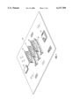
- FIG. 1 is a perspective view of a motherboard
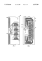
- FIG. 2 is a top plan view of the outside surface of an SO-RIMMs
- FIG. 3 is a top plan view of one of the layers of the RIMM shown in FIG. 2;
- FIG. 4 is a top plan view of another of the layers of the RIMM shown in FIG. 2;
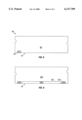
- FIG. 5 is a top plan view of the side of the RIMM, opposite the side shown in FIG. 2;
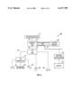
- FIG. 6 is a block diagram showing an example of a computer system for implementing one embodiment of the present invention.
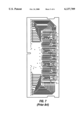
- FIG. 7 is a top plan view illustrating how the routing illustrated in FIGS. 2 through 7 might have been attempted using prior art techniques
- FIG. 8 is a top plan view of another embodiment of the invention.
- FIG. 9 is a bottom plan view of the embodiment shown in FIG. 8.
- a motherboard 10 for a computer system may include a plurality of electronic components such as a processor 12 and a plurality of in-line memory modules 14 coupled to a memory controller 15.
- the in-line memory modules may be Rambus in-line memory modules (RIMMs).
- the motherboard 10 may be adapted for use with a portable computer system.
- a portable computer system is a computer system of reduced size (compared to a desktop computer system) that may operate on battery power.
- Each RIMM includes a board 17 and an edge connector contacts 18.
- the board 17 mounts the integrated circuit Rambus memory chips 21.
- a first layer 16 may form one outer side of a board 17.
- the layer 16 may include edge connector contacts 18, in one embodiment of the invention, that extend along the length of the board 17.
- the contacts 18 couple the board 17 to the edge connector 19.
- the edge connector contacts 18 may include two portions 18a and 18b, extending along the length of the board 17.
- a plurality of electronic components indicated by the designators U1, U5, U4 and C1 through C8 may be attached to the board 17 using conventional PCB techniques.
- Conductors, traces, lines or routes 20 may extend from the edge connector contacts 18 to the electronic components including the chips 21.
- a plurality of integrated circuit Rambus memory chips may be secured to a PCB so that communication may occur between the edge connector 19 and the memory chips 21.
- the next layer within the board 17 is the layer 22 which may be spaced from the layer 16 by a dielectric material.
- the layer 22 may also include a plurality of routes 24 that may extend from the edge connector contacts 18 to the region, indicated as 26, where the memory chips 21 are mounted.
- a plurality of the routes 24 use "wrong-way” routing.
- the route 24a starts at the contact 28 and extends in a first direction parallel to the length of the edge connector contacts 18.
- the route 24a turns and at region 32, the route 24a extends back in the same direction, re-traversing the same area that it traversed between the contact 28 and the region 30.
- This type of routing is referred to as “wrong-way” routing and involves causing the route to extend along the length of the RIMM, parallel to the edge connector for a distance and then turning back in the opposite direction.
- Wrong-way routing may occur in the narrow turning region 34 of the RIMM which is a region of reduced available space in reduced area RIMM boards such as are used with portable computers.
- the region 30 may be defined by the edge connector contacts 18 and the region 26 used to mount the memory chips.
- the routes 24 extend through this region 34 from the edge connector contacts 18 to the bank of contacts 36. Thus, many of the routes extend across the region 34 in one direction, turn, and then extend in the opposite direction to come around the side of the chips to contact the contacts 36. With wrong-way routing, the routes, which need to go up in FIG. 3, actually first go down, then go up and then come around to contact the contacts 36.
- Wrong-way routing may advantageously allow the propagation delay of the sets of routes in a given layer to be matched by suitable length adjustments, improving the performance of the RIMM.
- wrong-way routing may facilitate the routing of the routes through the narrow turning region.
- a large gap may be used between the various signals and the propagation delay of routes is advantageously substantially equal.
- the thickness of the dielectric material between the layers 14 and 22, for example, may be approximately 0.005 inches to narrow the trace width of the routes. However, varying the thickness of the dielectric between the routes may also vary the propagation delay of the routing.
- serpentine routing for length matching may be disadvantageous in some embodiments because of the narrow turning region 34 that the routes traverse. Even though serpentine routing is an accepted approach to line lengthening, the density required by the portable RIMM board geometry makes wrong-way routing advantageous. wrong-way routing, in association with the short routes, may achieve added length given the small available area. Starting the route to the right (when needing to go left) and curving around, allows considerable length to be added to the shorter routes. Avoiding serpentine routing may decrease the number of turns that the signal follows, which may improve signal integrity.
- the layer 38 shown in. FIG. 4, is situated below the layer 22.
- serpentine routing had been used, in accordance with prior art techniques, instead of wrong-way routing, the routes corresponding to the conductors 24a, 24b and 24c would simply extend across the region 34 and turn around, as illustrated in FIG. 7.
- the routing shown in FIG. 7, may not achieve matching of the routing lengths. Therefore, a more elaborate serpentine pattern would need to be used but the available real estate does not readily permit such an approach.
- the outer layers such as the layers 16 and 40 may have a lower propagation delay time. Therefore, signals may move faster on these layers. Thus, the longest routes may be routed on the outer layers, shortening the overall delay.
- an embodiment of a computer system 50 in accordance with one embodiment of the invention includes a memory hub bridge circuit 52, which may include interfaces for a memory bus 54, a microprocessor bus 56, and an accelerated graphics port (AGP) 56 and a hub link 58.
- AGP is described in the Accelerated Graphics Port Interface Specification, Revision 1.0, published Jul. 31, 1996, by Intel Corporation, Santa Clara.
- the bridge circuit 52 may receive data from any one of the above described interfaces, and in response, the bridge circuit 52 may route the received data to another one of the interfaces.
- the computer system 50 may also include a microprocessor 12 that may be coupled to the bridge circuit 52 by the processor bus 56.
- a system memory 64 may be coupled to the bridge circuit by the memory bus 54.
- the system memory 64 may be comprised of the RIMMs 14 and memory controller 15 shown in FIG. 1.
- a graphics accelerator 68 may be coupled by the AGP 56 to the bridge circuit 52.
- An input/output bridge circuit 70 may be coupled to the bridge circuit 52 by the hub link 58.
- the bridge circuit 70 may provide an I/O interface for an I/O controller 76.
- the I/O controller 76 may be interfaced to the bridge circuit 70 by, for example, a bus 80 and the disk controller 78 may be interfaced to the bridge circuit 70 by, for example, another bus 74.
- the I/O controller may receive inputs from a mouse 82 and a keyboard 84.
- the I/O controller may also control operations of a floppy disk drive 86.
- the hub 70 may, for example, also control operations of a hard disk drive 88 and a compact disc read only memory (CD-ROM) drive 90.
- the graphics accelerator 68 may control operations of a display 92.
- signal lines and contacts 94 may be routed on one outer side 96 of the RIMM 14, in a common layer and the ground 98 and power supply lines and contacts 100 may be located in another layer 102 on the opposite side of the RIMM 14, as illustrated in FIGS. 8 and 9.
- the various signals which connect to the edge connector contacts 94, may be provided in an organization which differs from their pre-numbered sequence of conventional Rambus usage. For example, in conventional Rambus implementations, various signals are arranged consecutively in a predetermined pattern. The contacts associated with these signals are normally associated with one another in a sequential fashion as well. By mixing the arrangement of the pins to achieve an improved routing configuration, the performance of the RIMM may be improved.
- Locating the signals on one side may lessen the significance of the differences in inductance between pins on the top and bottom of the RIMM. With this arrangement, the inductance difference arises between signal and ground only, which simplifies the design of the connector and also simplifies routing.
- Having the signals on both sides of the connector may involve routing on one side of the RIMM board to compensate for differences introduced by the connector. Having all of the active signals on the same side of the RIMM may simplify the connector and may potentially save design time. By rearranging the order of the signals around the connector, the form factor may be reduced while the routing complexity may be lessened.
- routing can be divided into sections on each side of the RIMM.
- a routing pattern may be developed.
- the pin definition may allow the shortest length routing on the module. This may equate to smaller form factors for the module. Thus, a smaller form factor may be achieved with higher routing density.
Abstract
Description
______________________________________
          Pin                   Pin
Pin       Name      Pin         Name
______________________________________
 1        SPD.sub.-- CLK
                    38          DQB1.sub.-- R
 2        SPD.sub.-- DATA
                    39          DQB2.sub.-- R
 3        SCK       40          DQB3.sub.-- R
 4        SIO0      41          DQB4.sub.-- R
 5        DQA0.sub.-- L
                    42          DQB5.sub.-- R
 6        DQA1.sub.-- L
                    43          DQB6.sub.-- R
 7        DQA2.sub.-- L
                    44          DQB7.sub.-- R
 8        DQA3.sub.-- L
                    45          DQB8.sub.-- R
 9        DQA4.sub.-- L
                    46          RQ0.sub.-- R
10        DQA5.sub.-- L
                    47          RQ1.sub.-- R
11        DQA6.sub.-- L
                    48          RQ2.sub.-- R
12        DQA7.sub.-- L
                    49          RQ3.sub.-- R
13        DQA8.sub.-- L
                    50          RQ4.sub.-- R
14        CFM#      51          RQ5.sub.-- R
15        CFM       52          RQ6.sub.-- R
16        CTM#      53          RQ7.sub.-- R
17        CTM       54          CTM
18        RQ7.sub.-- L
                    55          CTM#
19        RQ6.sub.-- L
                    56          CFM
20        RQ5.sub.-- L
                    57          CFM#
21        RQ4.sub.-- L
                    58          DQA8.sub.-- R
22        RQ3.sub.-- L
                    59          DQA7.sub.-- R
23        RQ2.sub.-- L
                    60          DQA6.sub.-- R
24        RQ1.sub.-- L
                    61          DQA5.sub.-- R
25        RQ0.sub.-- L
                    62          DQA4.sub.-- R
26        DQB8.sub.-- L
                    63          DQA3.sub.-- R
27        DQB7.sub.-- L
                    64          DQA2.sub.-- R
28        DQB6.sub.-- L
                    65          DQA1.sub.-- R
29        DQB5.sub.-- L
                    66          DQA0.sub.-- R
30        DQB4.sub.-- L
                    67          SIO2
31        DQB3.sub.-- L
                    68          SCMD
32        DQB2.sub.-- L
                    69          SPD.sub.-- AD1
33        DQB1.sub.-- L
                    70          SPD.sub.-- AD0
34        DQB0.sub.-- L
                    A           VDD
35        V.sub.-- TT
                    B           GND
36        V.sub.-- REF
                    C           VDD
37        DQB0.sub.-- R
______________________________________
Claims (18)
Priority Applications (1)
| Application Number | Priority Date | Filing Date | Title |
|---|---|---|---|
| US09/499,084 US6137709A (en) | 1998-12-29 | 2000-02-04 | Small outline memory module |
Applications Claiming Priority (2)
| Application Number | Priority Date | Filing Date | Title |
|---|---|---|---|
| US09/221,804 US6061263A (en) | 1998-12-29 | 1998-12-29 | Small outline rambus in-line memory module |
| US09/499,084 US6137709A (en) | 1998-12-29 | 2000-02-04 | Small outline memory module |
Related Parent Applications (1)
| Application Number | Title | Priority Date | Filing Date |
|---|---|---|---|
| US09/221,804 Continuation US6061263A (en) | 1998-12-29 | 1998-12-29 | Small outline rambus in-line memory module |
Publications (1)
| Publication Number | Publication Date |
|---|---|
| US6137709A true US6137709A (en) | 2000-10-24 |
Family
ID=22829461
Family Applications (2)
| Application Number | Title | Priority Date | Filing Date |
|---|---|---|---|
| US09/221,804 Expired - Lifetime US6061263A (en) | 1998-12-29 | 1998-12-29 | Small outline rambus in-line memory module |
| US09/499,084 Expired - Lifetime US6137709A (en) | 1998-12-29 | 2000-02-04 | Small outline memory module |
Family Applications Before (1)
| Application Number | Title | Priority Date | Filing Date |
|---|---|---|---|
| US09/221,804 Expired - Lifetime US6061263A (en) | 1998-12-29 | 1998-12-29 | Small outline rambus in-line memory module |
Country Status (1)
| Country | Link |
|---|---|
| US (2) | US6061263A (en) |
Cited By (62)
| Publication number | Priority date | Publication date | Assignee | Title |
|---|---|---|---|---|
| US6317352B1 (en) * | 2000-09-18 | 2001-11-13 | Intel Corporation | Apparatus for implementing a buffered daisy chain connection between a memory controller and memory modules |
| US6362973B1 (en) * | 2000-03-14 | 2002-03-26 | Intel Corporation | Multilayer printed circuit board with placebo vias for controlling interconnect skew |
| US6366466B1 (en) * | 2000-03-14 | 2002-04-02 | Intel Corporation | Multi-layer printed circuit board with signal traces of varying width |
| US6426879B1 (en) * | 2000-10-20 | 2002-07-30 | Mitsubishi Denki Kabushiki Kaisha | Load adjustment board and data processing apparatus |
| US6449166B1 (en) * | 2000-08-24 | 2002-09-10 | High Connection Density, Inc. | High capacity memory module with higher density and improved manufacturability |
| US6461169B1 (en) | 2001-05-04 | 2002-10-08 | Intel Corporation | Interconnecting circuit modules to a motherboard using an edge connector with conductive polymer contacts |
| US6496400B2 (en) * | 1998-06-30 | 2002-12-17 | Micron Technology Inc. | Memory architecture and addressing for optimized density in integrated circuit package or on circuit board |
| US6542377B1 (en) * | 2000-06-28 | 2003-04-01 | Dell Products L.P. | Printed circuit assembly having conductive pad array with in-line via placement |
| KR20030073262A (en) * | 2002-03-09 | 2003-09-19 | 삼성전자주식회사 | Lay Out for SO-RIMM |
| US6654270B2 (en) * | 1999-05-12 | 2003-11-25 | Hitachi, Ltd. | Directional coupling memory module |
| US6657871B2 (en) * | 2000-05-10 | 2003-12-02 | Rambus Inc. | Multiple channel modules and bus systems using same |
| US20040003942A1 (en) * | 2002-07-02 | 2004-01-08 | Dell Products L.P. | System and method for minimizing a loading effect of a via by tuning a cutout ratio |
| US20040010661A1 (en) * | 1996-11-21 | 2004-01-15 | Hitachi, Ltd. | Disk array device with selectable method for generating redundant data |
| US20040190275A1 (en) * | 2000-10-18 | 2004-09-30 | Roscoe Brett D. | System for protecting electronic components |
| US20050066136A1 (en) * | 2003-09-18 | 2005-03-24 | Schnepper Randy L. | Memory hub with integrated non-volatile memory |
| US20050144403A1 (en) * | 2003-12-29 | 2005-06-30 | Jeddeloh Joseph M. | Memory hub and method for memory system performance monitoring |
| US20050146943A1 (en) * | 2003-08-28 | 2005-07-07 | Jeddeloh Joseph M. | Memory module and method having on-board data search capabilities and processor-based system using such memory modules |
| US20050177677A1 (en) * | 2004-02-05 | 2005-08-11 | Jeddeloh Joseph M. | Arbitration system having a packet memory and method for memory responses in a hub-based memory system |
| US20050219825A1 (en) * | 2004-03-31 | 2005-10-06 | Edoardo Campini | ATCA integrated heatsink and core power distribution mechanism |
| US6978328B1 (en) | 1999-05-12 | 2005-12-20 | Hitachi, Ltd. | Bus system, memory system, printed circuit board and directional coupler |
| US6980042B2 (en) | 2004-04-05 | 2005-12-27 | Micron Technology, Inc. | Delay line synchronizer apparatus and method |
| US7047351B2 (en) | 2002-08-16 | 2006-05-16 | Micron Technology, Inc. | Memory hub bypass circuit and method |
| US7102907B2 (en) | 2002-09-09 | 2006-09-05 | Micron Technology, Inc. | Wavelength division multiplexed memory module, memory system and method |
| US7107415B2 (en) | 2003-06-20 | 2006-09-12 | Micron Technology, Inc. | Posted write buffers and methods of posting write requests in memory modules |
| US7120743B2 (en) | 2003-10-20 | 2006-10-10 | Micron Technology, Inc. | Arbitration system and method for memory responses in a hub-based memory system |
| US7120727B2 (en) | 2003-06-19 | 2006-10-10 | Micron Technology, Inc. | Reconfigurable memory module and method |
| US7120723B2 (en) | 2004-03-25 | 2006-10-10 | Micron Technology, Inc. | System and method for memory hub-based expansion bus |
| US20060245119A1 (en) * | 2005-04-18 | 2006-11-02 | Goodwin June E | Memory module with a predetermined arrangement of pins |
| US7133972B2 (en) | 2002-06-07 | 2006-11-07 | Micron Technology, Inc. | Memory hub with internal cache and/or memory access prediction |
| US7133991B2 (en) | 2003-08-20 | 2006-11-07 | Micron Technology, Inc. | Method and system for capturing and bypassing memory transactions in a hub-based memory system |
| US7136958B2 (en) | 2003-08-28 | 2006-11-14 | Micron Technology, Inc. | Multiple processor system and method including multiple memory hub modules |
| US7162567B2 (en) | 2004-05-14 | 2007-01-09 | Micron Technology, Inc. | Memory hub and method for memory sequencing |
| US7180522B2 (en) | 2000-06-23 | 2007-02-20 | Micron Technology, Inc. | Apparatus and method for distributed memory control in a graphics processing system |
| US7181584B2 (en) | 2004-02-05 | 2007-02-20 | Micron Technology, Inc. | Dynamic command and/or address mirroring system and method for memory modules |
| US7188219B2 (en) | 2004-01-30 | 2007-03-06 | Micron Technology, Inc. | Buffer control system and method for a memory system having outstanding read and write request buffers |
| US7200024B2 (en) | 2002-08-02 | 2007-04-03 | Micron Technology, Inc. | System and method for optically interconnecting memory devices |
| US7210059B2 (en) | 2003-08-19 | 2007-04-24 | Micron Technology, Inc. | System and method for on-board diagnostics of memory modules |
| US7213082B2 (en) | 2004-03-29 | 2007-05-01 | Micron Technology, Inc. | Memory hub and method for providing memory sequencing hints |
| US7222213B2 (en) | 2004-05-17 | 2007-05-22 | Micron Technology, Inc. | System and method for communicating the synchronization status of memory modules during initialization of the memory modules |
| US7222197B2 (en) | 2003-07-22 | 2007-05-22 | Micron Technology, Inc. | Apparatus and method for direct memory access in a hub-based memory system |
| US7242213B2 (en) | 2003-06-11 | 2007-07-10 | Micron Technology, Inc. | Memory module and method having improved signal routing topology |
| US7249236B2 (en) | 2002-08-29 | 2007-07-24 | Micron Technology, Inc. | Method and system for controlling memory accesses to memory modules having a memory hub architecture |
| US7254331B2 (en) | 2002-08-09 | 2007-08-07 | Micron Technology, Inc. | System and method for multiple bit optical data transmission in memory systems |
| US7257683B2 (en) | 2004-03-24 | 2007-08-14 | Micron Technology, Inc. | Memory arbitration system and method having an arbitration packet protocol |
| US7260685B2 (en) | 2003-06-20 | 2007-08-21 | Micron Technology, Inc. | Memory hub and access method having internal prefetch buffers |
| US7310752B2 (en) | 2003-09-12 | 2007-12-18 | Micron Technology, Inc. | System and method for on-board timing margin testing of memory modules |
| US7310748B2 (en) | 2004-06-04 | 2007-12-18 | Micron Technology, Inc. | Memory hub tester interface and method for use thereof |
| US7330992B2 (en) | 2003-12-29 | 2008-02-12 | Micron Technology, Inc. | System and method for read synchronization of memory modules |
| US7363419B2 (en) | 2004-05-28 | 2008-04-22 | Micron Technology, Inc. | Method and system for terminating write commands in a hub-based memory system |
| US7366864B2 (en) | 2004-03-08 | 2008-04-29 | Micron Technology, Inc. | Memory hub architecture having programmable lane widths |
| US7392331B2 (en) | 2004-08-31 | 2008-06-24 | Micron Technology, Inc. | System and method for transmitting data packets in a computer system having a memory hub architecture |
| US20080158956A1 (en) * | 2006-12-29 | 2008-07-03 | Jeon-Taek Im | Non-volatile memory module for preventing system failure and system including the same |
| US7428644B2 (en) | 2003-06-20 | 2008-09-23 | Micron Technology, Inc. | System and method for selective memory module power management |
| US7447240B2 (en) | 2004-03-29 | 2008-11-04 | Micron Technology, Inc. | Method and system for synchronizing communications links in a hub-based memory system |
| US7519788B2 (en) | 2004-06-04 | 2009-04-14 | Micron Technology, Inc. | System and method for an asynchronous data buffer having buffer write and read pointers |
| US20090178829A1 (en) * | 2008-01-15 | 2009-07-16 | Wintex Corporation | Anti-breakage structure for transmitting end formed on flexible printed circuitboard |
| US7590797B2 (en) | 2004-04-08 | 2009-09-15 | Micron Technology, Inc. | System and method for optimizing interconnections of components in a multichip memory module |
| US20090267628A1 (en) * | 2008-02-26 | 2009-10-29 | Nec Electronics Corporation | Circuit board test system and test method |
| US7788451B2 (en) | 2004-02-05 | 2010-08-31 | Micron Technology, Inc. | Apparatus and method for data bypass for a bi-directional data bus in a hub-based memory sub-system |
| US7805586B2 (en) | 2002-08-29 | 2010-09-28 | Micron Technology, Inc. | System and method for optimizing interconnections of memory devices in a multichip module |
| US20100296256A1 (en) * | 2009-05-22 | 2010-11-25 | Mosaid Technologies Incorporated | Configurable module and memory subsystem |
| US8954687B2 (en) | 2002-08-05 | 2015-02-10 | Micron Technology, Inc. | Memory hub and access method having a sequencer and internal row caching |
Families Citing this family (8)
| Publication number | Priority date | Publication date | Assignee | Title |
|---|---|---|---|---|
| US6285962B1 (en) * | 1998-08-26 | 2001-09-04 | Tanisys Technology, Inc. | Method and system for testing rambus memory modules |
| US6061263A (en) * | 1998-12-29 | 2000-05-09 | Intel Corporation | Small outline rambus in-line memory module |
| AU1634600A (en) | 1998-12-30 | 2000-07-24 | Intel Corporation | Memory array organization |
| US6950891B1 (en) * | 1999-12-14 | 2005-09-27 | Intel Corporation | Signal routing between a memory control unit and a memory device |
| US20040030952A1 (en) * | 2000-09-29 | 2004-02-12 | Piccirillo Gary J. | Rambus based hot plug memory |
| US6535411B2 (en) | 2000-12-27 | 2003-03-18 | Intel Corporation | Memory module and computer system comprising a memory module |
| US6947304B1 (en) | 2003-05-12 | 2005-09-20 | Pericon Semiconductor Corp. | DDR memory modules with input buffers driving split traces with trace-impedance matching at trace junctions |
| US20060168407A1 (en) * | 2005-01-26 | 2006-07-27 | Micron Technology, Inc. | Memory hub system and method having large virtual page size |
Citations (2)
| Publication number | Priority date | Publication date | Assignee | Title |
|---|---|---|---|---|
| US3142047A (en) * | 1960-12-14 | 1964-07-21 | Columbia Broadcasting Systems | Memory plane |
| US6061263A (en) * | 1998-12-29 | 2000-05-09 | Intel Corporation | Small outline rambus in-line memory module |
Family Cites Families (1)
| Publication number | Priority date | Publication date | Assignee | Title |
|---|---|---|---|---|
| US5089993B1 (en) * | 1989-09-29 | 1998-12-01 | Texas Instruments Inc | Memory module arranged for data and parity bits |
-
1998
- 1998-12-29 US US09/221,804 patent/US6061263A/en not_active Expired - Lifetime
-
2000
- 2000-02-04 US US09/499,084 patent/US6137709A/en not_active Expired - Lifetime
Patent Citations (2)
| Publication number | Priority date | Publication date | Assignee | Title |
|---|---|---|---|---|
| US3142047A (en) * | 1960-12-14 | 1964-07-21 | Columbia Broadcasting Systems | Memory plane |
| US6061263A (en) * | 1998-12-29 | 2000-05-09 | Intel Corporation | Small outline rambus in-line memory module |
Cited By (171)
| Publication number | Priority date | Publication date | Assignee | Title |
|---|---|---|---|---|
| US20040010661A1 (en) * | 1996-11-21 | 2004-01-15 | Hitachi, Ltd. | Disk array device with selectable method for generating redundant data |
| US6496400B2 (en) * | 1998-06-30 | 2002-12-17 | Micron Technology Inc. | Memory architecture and addressing for optimized density in integrated circuit package or on circuit board |
| US6654270B2 (en) * | 1999-05-12 | 2003-11-25 | Hitachi, Ltd. | Directional coupling memory module |
| US6978328B1 (en) | 1999-05-12 | 2005-12-20 | Hitachi, Ltd. | Bus system, memory system, printed circuit board and directional coupler |
| US6366466B1 (en) * | 2000-03-14 | 2002-04-02 | Intel Corporation | Multi-layer printed circuit board with signal traces of varying width |
| US6362973B1 (en) * | 2000-03-14 | 2002-03-26 | Intel Corporation | Multilayer printed circuit board with placebo vias for controlling interconnect skew |
| US20070120575A1 (en) * | 2000-05-10 | 2007-05-31 | Rambus Inc. | Multiple Channel Modules and Bus Systems Using Same |
| US6657871B2 (en) * | 2000-05-10 | 2003-12-02 | Rambus Inc. | Multiple channel modules and bus systems using same |
| US7180522B2 (en) | 2000-06-23 | 2007-02-20 | Micron Technology, Inc. | Apparatus and method for distributed memory control in a graphics processing system |
| US6542377B1 (en) * | 2000-06-28 | 2003-04-01 | Dell Products L.P. | Printed circuit assembly having conductive pad array with in-line via placement |
| US6449166B1 (en) * | 2000-08-24 | 2002-09-10 | High Connection Density, Inc. | High capacity memory module with higher density and improved manufacturability |
| US6317352B1 (en) * | 2000-09-18 | 2001-11-13 | Intel Corporation | Apparatus for implementing a buffered daisy chain connection between a memory controller and memory modules |
| US20040190275A1 (en) * | 2000-10-18 | 2004-09-30 | Roscoe Brett D. | System for protecting electronic components |
| US7057901B2 (en) * | 2000-10-18 | 2006-06-06 | Hewlett-Packard Development Company, L.P. | System for protecting electronic components |
| US6426879B1 (en) * | 2000-10-20 | 2002-07-30 | Mitsubishi Denki Kabushiki Kaisha | Load adjustment board and data processing apparatus |
| US6461169B1 (en) | 2001-05-04 | 2002-10-08 | Intel Corporation | Interconnecting circuit modules to a motherboard using an edge connector with conductive polymer contacts |
| KR20030073262A (en) * | 2002-03-09 | 2003-09-19 | 삼성전자주식회사 | Lay Out for SO-RIMM |
| US7644253B2 (en) | 2002-06-07 | 2010-01-05 | Micron Technology, Inc. | Memory hub with internal cache and/or memory access prediction |
| US8499127B2 (en) | 2002-06-07 | 2013-07-30 | Round Rock Research, Llc | Memory hub with internal cache and/or memory access prediction |
| US8195918B2 (en) | 2002-06-07 | 2012-06-05 | Round Rock Research, Llc | Memory hub with internal cache and/or memory access prediction |
| US7133972B2 (en) | 2002-06-07 | 2006-11-07 | Micron Technology, Inc. | Memory hub with internal cache and/or memory access prediction |
| US20110219196A1 (en) * | 2002-06-07 | 2011-09-08 | Round Rock Research, Llc | Memory hub with internal cache and/or memory access prediction |
| US7945737B2 (en) | 2002-06-07 | 2011-05-17 | Round Rock Research, Llc | Memory hub with internal cache and/or memory access prediction |
| US6801880B2 (en) | 2002-07-02 | 2004-10-05 | Dell Products L.P. | System and method for minimizing a loading effect of a via by tuning a cutout ratio |
| US20040003942A1 (en) * | 2002-07-02 | 2004-01-08 | Dell Products L.P. | System and method for minimizing a loading effect of a via by tuning a cutout ratio |
| US7411807B2 (en) | 2002-08-02 | 2008-08-12 | Micron Technology, Inc. | System and method for optically interconnecting memory devices |
| US7382639B2 (en) | 2002-08-02 | 2008-06-03 | Micron Technology, Inc. | System and method for optically interconnecting memory devices |
| US7289347B2 (en) | 2002-08-02 | 2007-10-30 | Micron Technology, Inc. | System and method for optically interconnecting memory devices |
| US7200024B2 (en) | 2002-08-02 | 2007-04-03 | Micron Technology, Inc. | System and method for optically interconnecting memory devices |
| US8954687B2 (en) | 2002-08-05 | 2015-02-10 | Micron Technology, Inc. | Memory hub and access method having a sequencer and internal row caching |
| US7254331B2 (en) | 2002-08-09 | 2007-08-07 | Micron Technology, Inc. | System and method for multiple bit optical data transmission in memory systems |
| US7489875B2 (en) | 2002-08-09 | 2009-02-10 | Micron Technology, Inc. | System and method for multiple bit optical data transmission in memory systems |
| US7047351B2 (en) | 2002-08-16 | 2006-05-16 | Micron Technology, Inc. | Memory hub bypass circuit and method |
| US7149874B2 (en) | 2002-08-16 | 2006-12-12 | Micron Technology, Inc. | Memory hub bypass circuit and method |
| US7415567B2 (en) | 2002-08-16 | 2008-08-19 | Micron Technology, Inc. | Memory hub bypass circuit and method |
| US7716444B2 (en) | 2002-08-29 | 2010-05-11 | Round Rock Research, Llc | Method and system for controlling memory accesses to memory modules having a memory hub architecture |
| US8086815B2 (en) | 2002-08-29 | 2011-12-27 | Round Rock Research, Llc | System for controlling memory accesses to memory modules having a memory hub architecture |
| US7836252B2 (en) | 2002-08-29 | 2010-11-16 | Micron Technology, Inc. | System and method for optimizing interconnections of memory devices in a multichip module |
| US7908452B2 (en) | 2002-08-29 | 2011-03-15 | Round Rock Research, Llc | Method and system for controlling memory accesses to memory modules having a memory hub architecture |
| US7805586B2 (en) | 2002-08-29 | 2010-09-28 | Micron Technology, Inc. | System and method for optimizing interconnections of memory devices in a multichip module |
| US7249236B2 (en) | 2002-08-29 | 2007-07-24 | Micron Technology, Inc. | Method and system for controlling memory accesses to memory modules having a memory hub architecture |
| US8190819B2 (en) | 2002-08-29 | 2012-05-29 | Micron Technology, Inc. | System and method for optimizing interconnections of memory devices in a multichip module |
| US8234479B2 (en) | 2002-08-29 | 2012-07-31 | Round Rock Research, Llc | System for controlling memory accesses to memory modules having a memory hub architecture |
| US20110167238A1 (en) * | 2002-08-29 | 2011-07-07 | Round Rock Research, Llc | Method and system for controlling memory accesses to memory modules having a memory hub architecture |
| US7106611B2 (en) | 2002-09-09 | 2006-09-12 | Micron Technology, Inc. | Wavelength division multiplexed memory module, memory system and method |
| US7102907B2 (en) | 2002-09-09 | 2006-09-05 | Micron Technology, Inc. | Wavelength division multiplexed memory module, memory system and method |
| US7245145B2 (en) | 2003-06-11 | 2007-07-17 | Micron Technology, Inc. | Memory module and method having improved signal routing topology |
| US7282947B2 (en) | 2003-06-11 | 2007-10-16 | Micron Technology, Inc. | Memory module and method having improved signal routing topology |
| US7746095B2 (en) | 2003-06-11 | 2010-06-29 | Round Rock Research, Llc | Memory module and method having improved signal routing topology |
| US7242213B2 (en) | 2003-06-11 | 2007-07-10 | Micron Technology, Inc. | Memory module and method having improved signal routing topology |
| US7557601B2 (en) | 2003-06-11 | 2009-07-07 | Micron Technology, Inc. | Memory module and method having improved signal routing topology |
| US8200884B2 (en) | 2003-06-19 | 2012-06-12 | Round Rock Research, Llc | Reconfigurable memory module and method |
| US7966444B2 (en) | 2003-06-19 | 2011-06-21 | Round Rock Research, Llc | Reconfigurable memory module and method |
| US7120727B2 (en) | 2003-06-19 | 2006-10-10 | Micron Technology, Inc. | Reconfigurable memory module and method |
| US20110029746A1 (en) * | 2003-06-19 | 2011-02-03 | Round Rock Research, Llc | Reconfigurable memory module and method |
| US7818712B2 (en) | 2003-06-19 | 2010-10-19 | Round Rock Research, Llc | Reconfigurable memory module and method |
| US8732383B2 (en) | 2003-06-19 | 2014-05-20 | Round Rock Research, Llc | Reconfigurable memory module and method |
| US7529896B2 (en) | 2003-06-20 | 2009-05-05 | Micron Technology, Inc. | Memory modules having a memory hub containing a posted write buffer, a memory device interface and a link interface, and method of posting write requests in memory modules |
| US8127081B2 (en) | 2003-06-20 | 2012-02-28 | Round Rock Research, Llc | Memory hub and access method having internal prefetch buffers |
| US7107415B2 (en) | 2003-06-20 | 2006-09-12 | Micron Technology, Inc. | Posted write buffers and methods of posting write requests in memory modules |
| US7260685B2 (en) | 2003-06-20 | 2007-08-21 | Micron Technology, Inc. | Memory hub and access method having internal prefetch buffers |
| US7412566B2 (en) | 2003-06-20 | 2008-08-12 | Micron Technology, Inc. | Memory hub and access method having internal prefetch buffers |
| US7428644B2 (en) | 2003-06-20 | 2008-09-23 | Micron Technology, Inc. | System and method for selective memory module power management |
| US7437579B2 (en) | 2003-06-20 | 2008-10-14 | Micron Technology, Inc. | System and method for selective memory module power management |
| US7966430B2 (en) | 2003-07-22 | 2011-06-21 | Round Rock Research, Llc | Apparatus and method for direct memory access in a hub-based memory system |
| US7389364B2 (en) | 2003-07-22 | 2008-06-17 | Micron Technology, Inc. | Apparatus and method for direct memory access in a hub-based memory system |
| US7222197B2 (en) | 2003-07-22 | 2007-05-22 | Micron Technology, Inc. | Apparatus and method for direct memory access in a hub-based memory system |
| US8209445B2 (en) | 2003-07-22 | 2012-06-26 | Round Rock Research, Llc | Apparatus and method for direct memory access in a hub-based memory system |
| US7210059B2 (en) | 2003-08-19 | 2007-04-24 | Micron Technology, Inc. | System and method for on-board diagnostics of memory modules |
| US7278060B2 (en) | 2003-08-19 | 2007-10-02 | Micron Technology, Inc. | System and method for on-board diagnostics of memory modules |
| US7913122B2 (en) | 2003-08-19 | 2011-03-22 | Round Rock Research, Llc | System and method for on-board diagnostics of memory modules |
| US7516363B2 (en) | 2003-08-19 | 2009-04-07 | Micron Technology, Inc. | System and method for on-board diagnostics of memory modules |
| US7251714B2 (en) | 2003-08-20 | 2007-07-31 | Micron Technology, Inc. | Method and system for capturing and bypassing memory transactions in a hub-based memory system |
| US7133991B2 (en) | 2003-08-20 | 2006-11-07 | Micron Technology, Inc. | Method and system for capturing and bypassing memory transactions in a hub-based memory system |
| US20110113189A1 (en) * | 2003-08-28 | 2011-05-12 | Round Rock Research, Llc | Multiple processor system and method including multiple memory hub modules |
| US7136958B2 (en) | 2003-08-28 | 2006-11-14 | Micron Technology, Inc. | Multiple processor system and method including multiple memory hub modules |
| US7386649B2 (en) | 2003-08-28 | 2008-06-10 | Micron Technology, Inc. | Multiple processor system and method including multiple memory hub modules |
| US7581055B2 (en) | 2003-08-28 | 2009-08-25 | Micron Technology, Inc. | Multiple processor system and method including multiple memory hub modules |
| US8244952B2 (en) | 2003-08-28 | 2012-08-14 | Round Rock Research, Llc | Multiple processor system and method including multiple memory hub modules |
| US7873775B2 (en) | 2003-08-28 | 2011-01-18 | Round Rock Research, Llc | Multiple processor system and method including multiple memory hub modules |
| US20050146943A1 (en) * | 2003-08-28 | 2005-07-07 | Jeddeloh Joseph M. | Memory module and method having on-board data search capabilities and processor-based system using such memory modules |
| US9082461B2 (en) | 2003-08-28 | 2015-07-14 | Round Rock Research, Llc | Multiple processor system and method including multiple memory hub modules |
| US20100153794A1 (en) * | 2003-09-12 | 2010-06-17 | Round Rock Research, Llc | System and method for on-board timing margin testing of memory modules |
| US7958412B2 (en) | 2003-09-12 | 2011-06-07 | Round Rock Research, Llc | System and method for on-board timing margin testing of memory modules |
| US7689879B2 (en) | 2003-09-12 | 2010-03-30 | Micron Technology, Inc. | System and method for on-board timing margin testing of memory modules |
| US7310752B2 (en) | 2003-09-12 | 2007-12-18 | Micron Technology, Inc. | System and method for on-board timing margin testing of memory modules |
| US7194593B2 (en) | 2003-09-18 | 2007-03-20 | Micron Technology, Inc. | Memory hub with integrated non-volatile memory |
| US20050066136A1 (en) * | 2003-09-18 | 2005-03-24 | Schnepper Randy L. | Memory hub with integrated non-volatile memory |
| US7490211B2 (en) | 2003-09-18 | 2009-02-10 | Micron Technology, Inc. | Memory hub with integrated non-volatile memory |
| US7975122B2 (en) | 2003-09-18 | 2011-07-05 | Round Rock Research, Llc | Memory hub with integrated non-volatile memory |
| US8832404B2 (en) | 2003-09-18 | 2014-09-09 | Round Rock Research, Llc | Memory hub with integrated non-volatile memory |
| US7120743B2 (en) | 2003-10-20 | 2006-10-10 | Micron Technology, Inc. | Arbitration system and method for memory responses in a hub-based memory system |
| US8589643B2 (en) | 2003-10-20 | 2013-11-19 | Round Rock Research, Llc | Arbitration system and method for memory responses in a hub-based memory system |
| US7216196B2 (en) | 2003-12-29 | 2007-05-08 | Micron Technology, Inc. | Memory hub and method for memory system performance monitoring |
| US20050144403A1 (en) * | 2003-12-29 | 2005-06-30 | Jeddeloh Joseph M. | Memory hub and method for memory system performance monitoring |
| US7360011B2 (en) | 2003-12-29 | 2008-04-15 | Micron Technology, Inc. | Memory hub and method for memory system performance monitoring |
| US7330992B2 (en) | 2003-12-29 | 2008-02-12 | Micron Technology, Inc. | System and method for read synchronization of memory modules |
| US20080140904A1 (en) * | 2003-12-29 | 2008-06-12 | Micron Technology, Inc. | Memory hub and method for memory system performance monitoring |
| US7434081B2 (en) | 2003-12-29 | 2008-10-07 | Micron Technology, Inc. | System and method for read synchronization of memory modules |
| US7533213B2 (en) | 2003-12-29 | 2009-05-12 | Micron Technology, Inc. | Memory hub and method for memory system performance monitoring |
| US8880833B2 (en) | 2003-12-29 | 2014-11-04 | Micron Technology, Inc. | System and method for read synchronization of memory modules |
| US20070174562A1 (en) * | 2003-12-29 | 2007-07-26 | Micron Technology, Inc. | Memory hub and method for memory system performance monitoring |
| US8392686B2 (en) | 2003-12-29 | 2013-03-05 | Micron Technology, Inc. | System and method for read synchronization of memory modules |
| US8504782B2 (en) | 2004-01-30 | 2013-08-06 | Micron Technology, Inc. | Buffer control system and method for a memory system having outstanding read and write request buffers |
| US7188219B2 (en) | 2004-01-30 | 2007-03-06 | Micron Technology, Inc. | Buffer control system and method for a memory system having outstanding read and write request buffers |
| US8788765B2 (en) | 2004-01-30 | 2014-07-22 | Micron Technology, Inc. | Buffer control system and method for a memory system having outstanding read and write request buffers |
| US8291173B2 (en) | 2004-02-05 | 2012-10-16 | Micron Technology, Inc. | Apparatus and method for data bypass for a bi-directional data bus in a hub-based memory sub-system |
| US8694735B2 (en) | 2004-02-05 | 2014-04-08 | Micron Technology, Inc. | Apparatus and method for data bypass for a bi-directional data bus in a hub-based memory sub-system |
| US7181584B2 (en) | 2004-02-05 | 2007-02-20 | Micron Technology, Inc. | Dynamic command and/or address mirroring system and method for memory modules |
| US7788451B2 (en) | 2004-02-05 | 2010-08-31 | Micron Technology, Inc. | Apparatus and method for data bypass for a bi-directional data bus in a hub-based memory sub-system |
| US7412574B2 (en) | 2004-02-05 | 2008-08-12 | Micron Technology, Inc. | System and method for arbitration of memory responses in a hub-based memory system |
| US9164937B2 (en) | 2004-02-05 | 2015-10-20 | Micron Technology, Inc. | Apparatus and method for data bypass for a bi-directional data bus in a hub-based memory sub-system |
| US7546435B2 (en) | 2004-02-05 | 2009-06-09 | Micron Technology. Inc. | Dynamic command and/or address mirroring system and method for memory modules |
| US20050177677A1 (en) * | 2004-02-05 | 2005-08-11 | Jeddeloh Joseph M. | Arbitration system having a packet memory and method for memory responses in a hub-based memory system |
| US7366864B2 (en) | 2004-03-08 | 2008-04-29 | Micron Technology, Inc. | Memory hub architecture having programmable lane widths |
| US7596675B2 (en) | 2004-03-08 | 2009-09-29 | Micron Technology, Inc. | Memory hub architecture having programmable lane widths |
| US20080162861A1 (en) * | 2004-03-08 | 2008-07-03 | Micron Technology, Inc. | Memory hub architecture having programmable lane widths |
| US8775764B2 (en) | 2004-03-08 | 2014-07-08 | Micron Technology, Inc. | Memory hub architecture having programmable lane widths |
| US9274991B2 (en) | 2004-03-08 | 2016-03-01 | Micron Technology, Inc. | Memory hub architecture having programmable lane widths |
| US8015384B2 (en) | 2004-03-08 | 2011-09-06 | Micron Technology, Inc. | Memory hub architecture having programmable lane widths |
| US7412571B2 (en) | 2004-03-24 | 2008-08-12 | Micron Technology, Inc. | Memory arbitration system and method having an arbitration packet protocol |
| US8555006B2 (en) | 2004-03-24 | 2013-10-08 | Micron Technology, Inc. | Memory arbitration system and method having an arbitration packet protocol |
| US7257683B2 (en) | 2004-03-24 | 2007-08-14 | Micron Technology, Inc. | Memory arbitration system and method having an arbitration packet protocol |
| US8082404B2 (en) | 2004-03-24 | 2011-12-20 | Micron Technology, Inc. | Memory arbitration system and method having an arbitration packet protocol |
| US9032166B2 (en) | 2004-03-24 | 2015-05-12 | Micron Technology, Inc. | Memory arbitration system and method having an arbitration packet protocol |
| US7206887B2 (en) | 2004-03-25 | 2007-04-17 | Micron Technology, Inc. | System and method for memory hub-based expansion bus |
| US7120723B2 (en) | 2004-03-25 | 2006-10-10 | Micron Technology, Inc. | System and method for memory hub-based expansion bus |
| US7370134B2 (en) | 2004-03-25 | 2008-05-06 | Micron Technology, Inc. | System and method for memory hub-based expansion bus |
| US7899969B2 (en) | 2004-03-25 | 2011-03-01 | Round Rock Research, Llc | System and method for memory hub-based expansion bus |
| US7610430B2 (en) | 2004-03-25 | 2009-10-27 | Micron Technology, Inc. | System and method for memory hub-based expansion bus |
| US7222210B2 (en) | 2004-03-25 | 2007-05-22 | Micron Technology, Inc. | System and method for memory hub-based expansion bus |
| US7174409B2 (en) | 2004-03-25 | 2007-02-06 | Micron Technology, Inc. | System and method for memory hub-based expansion bus |
| US8117371B2 (en) | 2004-03-25 | 2012-02-14 | Round Rock Research, Llc | System and method for memory hub-based expansion bus |
| US7418526B2 (en) | 2004-03-29 | 2008-08-26 | Micron Technology, Inc. | Memory hub and method for providing memory sequencing hints |
| US7213082B2 (en) | 2004-03-29 | 2007-05-01 | Micron Technology, Inc. | Memory hub and method for providing memory sequencing hints |
| US7529273B2 (en) | 2004-03-29 | 2009-05-05 | Micron Technology, Inc. | Method and system for synchronizing communications links in a hub-based memory system |
| US7447240B2 (en) | 2004-03-29 | 2008-11-04 | Micron Technology, Inc. | Method and system for synchronizing communications links in a hub-based memory system |
| US20050219825A1 (en) * | 2004-03-31 | 2005-10-06 | Edoardo Campini | ATCA integrated heatsink and core power distribution mechanism |
| US7133287B2 (en) * | 2004-03-31 | 2006-11-07 | Intel Corporation | ATCA integrated heatsink and core power distribution mechanism |
| US8164375B2 (en) | 2004-04-05 | 2012-04-24 | Round Rock Research, Llc | Delay line synchronizer apparatus and method |
| US7605631B2 (en) | 2004-04-05 | 2009-10-20 | Micron Technology, Inc. | Delay line synchronizer apparatus and method |
| US6980042B2 (en) | 2004-04-05 | 2005-12-27 | Micron Technology, Inc. | Delay line synchronizer apparatus and method |
| US7870329B2 (en) | 2004-04-08 | 2011-01-11 | Micron Technology, Inc. | System and method for optimizing interconnections of components in a multichip memory module |
| US8438329B2 (en) | 2004-04-08 | 2013-05-07 | Micron Technology, Inc. | System and method for optimizing interconnections of components in a multichip memory module |
| US7590797B2 (en) | 2004-04-08 | 2009-09-15 | Micron Technology, Inc. | System and method for optimizing interconnections of components in a multichip memory module |
| US7162567B2 (en) | 2004-05-14 | 2007-01-09 | Micron Technology, Inc. | Memory hub and method for memory sequencing |
| US7353320B2 (en) | 2004-05-14 | 2008-04-01 | Micron Technology, Inc. | Memory hub and method for memory sequencing |
| US7562178B2 (en) | 2004-05-14 | 2009-07-14 | Micron Technology, Inc. | Memory hub and method for memory sequencing |
| US7222213B2 (en) | 2004-05-17 | 2007-05-22 | Micron Technology, Inc. | System and method for communicating the synchronization status of memory modules during initialization of the memory modules |
| US7266633B2 (en) | 2004-05-17 | 2007-09-04 | Micron Technology, Inc. | System and method for communicating the synchronization status of memory modules during initialization of the memory modules |
| US7363419B2 (en) | 2004-05-28 | 2008-04-22 | Micron Technology, Inc. | Method and system for terminating write commands in a hub-based memory system |
| US7774559B2 (en) | 2004-05-28 | 2010-08-10 | Micron Technology, Inc. | Method and system for terminating write commands in a hub-based memory system |
| US7823024B2 (en) | 2004-06-04 | 2010-10-26 | Micron Technology, Inc. | Memory hub tester interface and method for use thereof |
| US7519788B2 (en) | 2004-06-04 | 2009-04-14 | Micron Technology, Inc. | System and method for an asynchronous data buffer having buffer write and read pointers |
| US7594088B2 (en) | 2004-06-04 | 2009-09-22 | Micron Technology, Inc. | System and method for an asynchronous data buffer having buffer write and read pointers |
| US8239607B2 (en) | 2004-06-04 | 2012-08-07 | Micron Technology, Inc. | System and method for an asynchronous data buffer having buffer write and read pointers |
| US7310748B2 (en) | 2004-06-04 | 2007-12-18 | Micron Technology, Inc. | Memory hub tester interface and method for use thereof |
| US7596641B2 (en) | 2004-08-31 | 2009-09-29 | Micron Technology, Inc. | System and method for transmitting data packets in a computer system having a memory hub architecture |
| US7392331B2 (en) | 2004-08-31 | 2008-06-24 | Micron Technology, Inc. | System and method for transmitting data packets in a computer system having a memory hub architecture |
| US8346998B2 (en) | 2004-08-31 | 2013-01-01 | Micron Technology, Inc. | System and method for transmitting data packets in a computer system having a memory hub architecture |
| US7949803B2 (en) | 2004-08-31 | 2011-05-24 | Micron Technology, Inc. | System and method for transmitting data packets in a computer system having a memory hub architecture |
| US7545651B2 (en) * | 2005-04-18 | 2009-06-09 | Hewlett-Packard Development Company, L.P. | Memory module with a predetermined arrangement of pins |
| US20060245119A1 (en) * | 2005-04-18 | 2006-11-02 | Goodwin June E | Memory module with a predetermined arrangement of pins |
| US20080158956A1 (en) * | 2006-12-29 | 2008-07-03 | Jeon-Taek Im | Non-volatile memory module for preventing system failure and system including the same |
| US7733680B2 (en) * | 2006-12-29 | 2010-06-08 | Samsung Electronics Co., Ltd. | Non-volatile memory module for preventing system failure and system including the same |
| US20090178829A1 (en) * | 2008-01-15 | 2009-07-16 | Wintex Corporation | Anti-breakage structure for transmitting end formed on flexible printed circuitboard |
| US20090267628A1 (en) * | 2008-02-26 | 2009-10-29 | Nec Electronics Corporation | Circuit board test system and test method |
| US8008940B2 (en) * | 2008-02-26 | 2011-08-30 | Renesas Electronics Corporation | Circuit board test system and test method |
| US20100296256A1 (en) * | 2009-05-22 | 2010-11-25 | Mosaid Technologies Incorporated | Configurable module and memory subsystem |
| US8767430B2 (en) * | 2009-05-22 | 2014-07-01 | Conversant Intellectual Property Management Inc. | Configurable module and memory subsystem |
| US8503211B2 (en) * | 2009-05-22 | 2013-08-06 | Mosaid Technologies Incorporated | Configurable module and memory subsystem |
Also Published As
| Publication number | Publication date |
|---|---|
| US6061263A (en) | 2000-05-09 |
Similar Documents
| Publication | Publication Date | Title |
|---|---|---|
| US6137709A (en) | Small outline memory module | |
| KR100900909B1 (en) | Buffer chip for a multi-rank dual inline memory module | |
| US7870329B2 (en) | System and method for optimizing interconnections of components in a multichip memory module | |
| TW539952B (en) | Memory system | |
| US6202110B1 (en) | Memory cards with symmetrical pinout for back-to-back mounting in computer system | |
| KR100290445B1 (en) | Memory module and socket for same | |
| US6067594A (en) | High frequency bus system | |
| US6567870B1 (en) | Apparatus and method for stacking cards for a computer | |
| US6978333B2 (en) | Method and system for reducing aggregate impedance discontinuity between expansion connectors | |
| US6771515B2 (en) | Systems having modules with on die terminations | |
| US7212424B2 (en) | Double-high DIMM with dual registers and related methods | |
| US6553555B1 (en) | Maintaining signal guard bands when routing through a field of obstacles | |
| US7405634B2 (en) | Method for altering the delay properties of a transmission line using compensation tabs | |
| US20040100812A1 (en) | Circuit topology for high speed memory access | |
| US20210103791A1 (en) | Card type solid state drive | |
| US7305509B2 (en) | Method and apparatus for zero stub serial termination capacitor of resistor mounting option in an information handling system | |
| US6995985B2 (en) | Power plane region of printed circuit board with power blocks having an arc-shaped boundary | |
| US6724082B2 (en) | Systems having modules with selectable on die terminations | |
| US6711027B2 (en) | Modules having paths of different impedances | |
| US6097619A (en) | Symmetric memory board | |
| EP1072066B1 (en) | A high speed bus contact system | |
| US6717823B2 (en) | Systems having modules with buffer chips | |
| US6081862A (en) | Switching system for optimization of signal reflection | |
| US7269028B2 (en) | Trace-pad interface for improved signal quality | |
| US20030016549A1 (en) | Systems with modules and clocking therefore |
Legal Events
| Date | Code | Title | Description |
|---|---|---|---|
| AS | Assignment |
Owner name: MICROSOFT CORPORATION, WASHINGTON Free format text: INVALID ASSIGNMENT;ASSIGNOR:BURNS, GREGORY;REEL/FRAME:010596/0393 Effective date: 20000201 |
|
| STCF | Information on status: patent grant |
Free format text: PATENTED CASE |
|
| FEPP | Fee payment procedure |
Free format text: PAYOR NUMBER ASSIGNED (ORIGINAL EVENT CODE: ASPN); ENTITY STATUS OF PATENT OWNER: LARGE ENTITY |
|
| FPAY | Fee payment |
Year of fee payment: 4 |
|
| FPAY | Fee payment |
Year of fee payment: 8 |
|
| FPAY | Fee payment |
Year of fee payment: 12 |
|
| FEPP | Fee payment procedure |
Free format text: PAYOR NUMBER ASSIGNED (ORIGINAL EVENT CODE: ASPN); ENTITY STATUS OF PATENT OWNER: LARGE ENTITY Free format text: PAYER NUMBER DE-ASSIGNED (ORIGINAL EVENT CODE: RMPN); ENTITY STATUS OF PATENT OWNER: LARGE ENTITY |
|
| AS | Assignment |
Owner name: ROUND ROCK RESEARCH, LLC, NEW JERSEY Free format text: ASSIGNMENT OF ASSIGNORS INTEREST;ASSIGNOR:MICRON TECHNOLOGY, INC.;REEL/FRAME:032765/0312 Effective date: 20140422 |