US5960270A - Method for forming an MOS transistor having a metallic gate electrode that is formed after the formation of self-aligned source and drain regions - Google Patents
Method for forming an MOS transistor having a metallic gate electrode that is formed after the formation of self-aligned source and drain regions Download PDFInfo
- Publication number
- US5960270A US5960270A US08/907,990 US90799097A US5960270A US 5960270 A US5960270 A US 5960270A US 90799097 A US90799097 A US 90799097A US 5960270 A US5960270 A US 5960270A
- Authority
- US
- United States
- Prior art keywords
- forming
- region
- opening
- feature
- gate
- Prior art date
- Legal status (The legal status is an assumption and is not a legal conclusion. Google has not performed a legal analysis and makes no representation as to the accuracy of the status listed.)
- Expired - Lifetime
Links
- 238000000034 method Methods 0.000 title claims abstract description 106
- 230000015572 biosynthetic process Effects 0.000 title claims abstract description 33
- 229910052751 metal Inorganic materials 0.000 claims abstract description 96
- 239000002184 metal Substances 0.000 claims abstract description 96
- 239000000758 substrate Substances 0.000 claims abstract description 46
- 230000009977 dual effect Effects 0.000 claims abstract description 24
- 229910021420 polycrystalline silicon Inorganic materials 0.000 claims description 50
- 229920005591 polysilicon Polymers 0.000 claims description 50
- 230000008569 process Effects 0.000 claims description 50
- 239000004065 semiconductor Substances 0.000 claims description 47
- 239000002019 doping agent Substances 0.000 claims description 42
- 229910021332 silicide Inorganic materials 0.000 claims description 41
- FVBUAEGBCNSCDD-UHFFFAOYSA-N silicide(4-) Chemical group [Si-4] FVBUAEGBCNSCDD-UHFFFAOYSA-N 0.000 claims description 38
- 239000000463 material Substances 0.000 claims description 20
- 150000002500 ions Chemical class 0.000 claims description 19
- 239000007769 metal material Substances 0.000 claims description 17
- 239000007943 implant Substances 0.000 claims description 16
- 125000006850 spacer group Chemical group 0.000 claims description 13
- 239000002131 composite material Substances 0.000 claims description 11
- 238000005530 etching Methods 0.000 claims description 11
- 238000005468 ion implantation Methods 0.000 claims description 11
- 239000000126 substance Substances 0.000 claims description 11
- 238000002955 isolation Methods 0.000 claims description 8
- ZOKXTWBITQBERF-UHFFFAOYSA-N Molybdenum Chemical compound [Mo] ZOKXTWBITQBERF-UHFFFAOYSA-N 0.000 claims description 7
- 229910052581 Si3N4 Inorganic materials 0.000 claims description 7
- 238000009792 diffusion process Methods 0.000 claims description 7
- 229910052750 molybdenum Inorganic materials 0.000 claims description 7
- 239000011733 molybdenum Substances 0.000 claims description 7
- 238000005498 polishing Methods 0.000 claims description 7
- WFKWXMTUELFFGS-UHFFFAOYSA-N tungsten Chemical compound [W] WFKWXMTUELFFGS-UHFFFAOYSA-N 0.000 claims description 7
- 229910052721 tungsten Inorganic materials 0.000 claims description 7
- 239000010937 tungsten Substances 0.000 claims description 7
- 229910021341 titanium silicide Inorganic materials 0.000 claims description 6
- NRTOMJZYCJJWKI-UHFFFAOYSA-N Titanium nitride Chemical compound [Ti]#N NRTOMJZYCJJWKI-UHFFFAOYSA-N 0.000 claims description 5
- 239000003990 capacitor Substances 0.000 claims description 5
- WQJQOUPTWCFRMM-UHFFFAOYSA-N tungsten disilicide Chemical compound [Si]#[W]#[Si] WQJQOUPTWCFRMM-UHFFFAOYSA-N 0.000 claims description 5
- 229910021342 tungsten silicide Inorganic materials 0.000 claims description 5
- 229910052785 arsenic Inorganic materials 0.000 claims description 4
- RQNWIZPPADIBDY-UHFFFAOYSA-N arsenic atom Chemical compound [As] RQNWIZPPADIBDY-UHFFFAOYSA-N 0.000 claims description 4
- 238000000151 deposition Methods 0.000 claims description 4
- HQVNEWCFYHHQES-UHFFFAOYSA-N silicon nitride Chemical compound N12[Si]34N5[Si]62N3[Si]51N64 HQVNEWCFYHHQES-UHFFFAOYSA-N 0.000 claims description 4
- 239000011800 void material Substances 0.000 claims description 4
- ZOXJGFHDIHLPTG-UHFFFAOYSA-N Boron Chemical compound [B] ZOXJGFHDIHLPTG-UHFFFAOYSA-N 0.000 claims description 3
- GWEVSGVZZGPLCZ-UHFFFAOYSA-N Titan oxide Chemical compound O=[Ti]=O GWEVSGVZZGPLCZ-UHFFFAOYSA-N 0.000 claims description 3
- KMTYGNUPYSXKGJ-UHFFFAOYSA-N [Si+4].[Si+4].[Ni++] Chemical compound [Si+4].[Si+4].[Ni++] KMTYGNUPYSXKGJ-UHFFFAOYSA-N 0.000 claims description 3
- 229910052796 boron Inorganic materials 0.000 claims description 3
- 239000010941 cobalt Substances 0.000 claims description 3
- 229910017052 cobalt Inorganic materials 0.000 claims description 3
- 229910044991 metal oxide Inorganic materials 0.000 claims description 3
- 150000004706 metal oxides Chemical class 0.000 claims description 3
- 229910052698 phosphorus Inorganic materials 0.000 claims description 3
- OAICVXFJPJFONN-UHFFFAOYSA-N Phosphorus Chemical compound [P] OAICVXFJPJFONN-UHFFFAOYSA-N 0.000 claims description 2
- 229910004446 Ta2 O5 Inorganic materials 0.000 claims description 2
- 229910008814 WSi2 Inorganic materials 0.000 claims description 2
- 229910021417 amorphous silicon Inorganic materials 0.000 claims description 2
- BHEPBYXIRTUNPN-UHFFFAOYSA-N hydridophosphorus(.) (triplet) Chemical compound [PH] BHEPBYXIRTUNPN-UHFFFAOYSA-N 0.000 claims description 2
- 239000011574 phosphorus Substances 0.000 claims description 2
- 238000007517 polishing process Methods 0.000 claims 2
- 229910021334 nickel silicide Inorganic materials 0.000 claims 1
- RUFLMLWJRZAWLJ-UHFFFAOYSA-N nickel silicide Chemical group [Ni]=[Si]=[Ni] RUFLMLWJRZAWLJ-UHFFFAOYSA-N 0.000 claims 1
- 238000005755 formation reaction Methods 0.000 description 29
- 150000004767 nitrides Chemical class 0.000 description 18
- 229920002120 photoresistant polymer Polymers 0.000 description 15
- XUIMIQQOPSSXEZ-UHFFFAOYSA-N Silicon Chemical compound [Si] XUIMIQQOPSSXEZ-UHFFFAOYSA-N 0.000 description 10
- 229910052710 silicon Inorganic materials 0.000 description 10
- 239000010703 silicon Substances 0.000 description 10
- 239000003989 dielectric material Substances 0.000 description 7
- 230000003647 oxidation Effects 0.000 description 6
- 238000007254 oxidation reaction Methods 0.000 description 6
- BOTDANWDWHJENH-UHFFFAOYSA-N Tetraethyl orthosilicate Chemical compound CCO[Si](OCC)(OCC)OCC BOTDANWDWHJENH-UHFFFAOYSA-N 0.000 description 4
- 230000002411 adverse Effects 0.000 description 4
- 238000010586 diagram Methods 0.000 description 4
- 238000005516 engineering process Methods 0.000 description 4
- 239000012535 impurity Substances 0.000 description 4
- 239000012212 insulator Substances 0.000 description 4
- 238000001465 metallisation Methods 0.000 description 4
- 239000006117 anti-reflective coating Substances 0.000 description 3
- 230000000903 blocking effect Effects 0.000 description 3
- 230000003993 interaction Effects 0.000 description 3
- 230000000873 masking effect Effects 0.000 description 3
- 230000037230 mobility Effects 0.000 description 3
- 238000004544 sputter deposition Methods 0.000 description 3
- ZAMOUSCENKQFHK-UHFFFAOYSA-N Chlorine atom Chemical compound [Cl] ZAMOUSCENKQFHK-UHFFFAOYSA-N 0.000 description 2
- VYPSYNLAJGMNEJ-UHFFFAOYSA-N Silicium dioxide Chemical compound O=[Si]=O VYPSYNLAJGMNEJ-UHFFFAOYSA-N 0.000 description 2
- 239000005380 borophosphosilicate glass Substances 0.000 description 2
- 230000015556 catabolic process Effects 0.000 description 2
- 239000000460 chlorine Substances 0.000 description 2
- 229910052801 chlorine Inorganic materials 0.000 description 2
- GUTLYIVDDKVIGB-UHFFFAOYSA-N cobalt atom Chemical compound [Co] GUTLYIVDDKVIGB-UHFFFAOYSA-N 0.000 description 2
- 238000006731 degradation reaction Methods 0.000 description 2
- 230000008021 deposition Effects 0.000 description 2
- 230000000694 effects Effects 0.000 description 2
- 238000012986 modification Methods 0.000 description 2
- 230000004048 modification Effects 0.000 description 2
- UPSOBXZLFLJAKK-UHFFFAOYSA-N ozone;tetraethyl silicate Chemical compound [O-][O+]=O.CCO[Si](OCC)(OCC)OCC UPSOBXZLFLJAKK-UHFFFAOYSA-N 0.000 description 2
- 238000000059 patterning Methods 0.000 description 2
- 239000003870 refractory metal Substances 0.000 description 2
- 241000894007 species Species 0.000 description 2
- JBRZTFJDHDCESZ-UHFFFAOYSA-N AsGa Chemical compound [As]#[Ga] JBRZTFJDHDCESZ-UHFFFAOYSA-N 0.000 description 1
- 241000252506 Characiformes Species 0.000 description 1
- XPDWGBQVDMORPB-UHFFFAOYSA-N Fluoroform Chemical compound FC(F)F XPDWGBQVDMORPB-UHFFFAOYSA-N 0.000 description 1
- 229910001218 Gallium arsenide Inorganic materials 0.000 description 1
- GPXJNWSHGFTCBW-UHFFFAOYSA-N Indium phosphide Chemical compound [In]#P GPXJNWSHGFTCBW-UHFFFAOYSA-N 0.000 description 1
- LEVVHYCKPQWKOP-UHFFFAOYSA-N [Si].[Ge] Chemical compound [Si].[Ge] LEVVHYCKPQWKOP-UHFFFAOYSA-N 0.000 description 1
- 229910052787 antimony Inorganic materials 0.000 description 1
- WATWJIUSRGPENY-UHFFFAOYSA-N antimony atom Chemical compound [Sb] WATWJIUSRGPENY-UHFFFAOYSA-N 0.000 description 1
- 239000000969 carrier Substances 0.000 description 1
- 150000001875 compounds Chemical class 0.000 description 1
- 229910021419 crystalline silicon Inorganic materials 0.000 description 1
- 230000032798 delamination Effects 0.000 description 1
- 238000005137 deposition process Methods 0.000 description 1
- 230000008030 elimination Effects 0.000 description 1
- 238000003379 elimination reaction Methods 0.000 description 1
- 229910052732 germanium Inorganic materials 0.000 description 1
- GNPVGFCGXDBREM-UHFFFAOYSA-N germanium atom Chemical compound [Ge] GNPVGFCGXDBREM-UHFFFAOYSA-N 0.000 description 1
- 229910052738 indium Inorganic materials 0.000 description 1
- APFVFJFRJDLVQX-UHFFFAOYSA-N indium atom Chemical compound [In] APFVFJFRJDLVQX-UHFFFAOYSA-N 0.000 description 1
- 229910000765 intermetallic Inorganic materials 0.000 description 1
- 238000004519 manufacturing process Methods 0.000 description 1
- 150000002739 metals Chemical class 0.000 description 1
- 239000000203 mixture Substances 0.000 description 1
- 229910052757 nitrogen Inorganic materials 0.000 description 1
- BPUBBGLMJRNUCC-UHFFFAOYSA-N oxygen(2-);tantalum(5+) Chemical compound [O-2].[O-2].[O-2].[O-2].[O-2].[Ta+5].[Ta+5] BPUBBGLMJRNUCC-UHFFFAOYSA-N 0.000 description 1
- 238000001020 plasma etching Methods 0.000 description 1
- 230000009467 reduction Effects 0.000 description 1
- HBMJWWWQQXIZIP-UHFFFAOYSA-N silicon carbide Chemical compound [Si+]#[C-] HBMJWWWQQXIZIP-UHFFFAOYSA-N 0.000 description 1
- 229910010271 silicon carbide Inorganic materials 0.000 description 1
- 235000012239 silicon dioxide Nutrition 0.000 description 1
- 239000000377 silicon dioxide Substances 0.000 description 1
- PBCFLUZVCVVTBY-UHFFFAOYSA-N tantalum pentoxide Inorganic materials O=[Ta](=O)O[Ta](=O)=O PBCFLUZVCVVTBY-UHFFFAOYSA-N 0.000 description 1
Images


Classifications
-
- H—ELECTRICITY
- H01—ELECTRIC ELEMENTS
- H01L—SEMICONDUCTOR DEVICES NOT COVERED BY CLASS H10
- H01L29/00—Semiconductor devices adapted for rectifying, amplifying, oscillating or switching, or capacitors or resistors with at least one potential-jump barrier or surface barrier, e.g. PN junction depletion layer or carrier concentration layer; Details of semiconductor bodies or of electrodes thereof ; Multistep manufacturing processes therefor
- H01L29/66—Types of semiconductor device ; Multistep manufacturing processes therefor
- H01L29/66007—Multistep manufacturing processes
- H01L29/66075—Multistep manufacturing processes of devices having semiconductor bodies comprising group 14 or group 13/15 materials
- H01L29/66227—Multistep manufacturing processes of devices having semiconductor bodies comprising group 14 or group 13/15 materials the devices being controllable only by the electric current supplied or the electric potential applied, to an electrode which does not carry the current to be rectified, amplified or switched, e.g. three-terminal devices
- H01L29/66409—Unipolar field-effect transistors
- H01L29/66477—Unipolar field-effect transistors with an insulated gate, i.e. MISFET
- H01L29/66568—Lateral single gate silicon transistors
- H01L29/66575—Lateral single gate silicon transistors where the source and drain or source and drain extensions are self-aligned to the sides of the gate
- H01L29/66583—Lateral single gate silicon transistors where the source and drain or source and drain extensions are self-aligned to the sides of the gate with initial gate mask or masking layer complementary to the prospective gate location, e.g. with dummy source and drain contacts
-
- H—ELECTRICITY
- H01—ELECTRIC ELEMENTS
- H01L—SEMICONDUCTOR DEVICES NOT COVERED BY CLASS H10
- H01L21/00—Processes or apparatus adapted for the manufacture or treatment of semiconductor or solid state devices or of parts thereof
- H01L21/02—Manufacture or treatment of semiconductor devices or of parts thereof
- H01L21/04—Manufacture or treatment of semiconductor devices or of parts thereof the devices having at least one potential-jump barrier or surface barrier, e.g. PN junction, depletion layer or carrier concentration layer
- H01L21/18—Manufacture or treatment of semiconductor devices or of parts thereof the devices having at least one potential-jump barrier or surface barrier, e.g. PN junction, depletion layer or carrier concentration layer the devices having semiconductor bodies comprising elements of Group IV of the Periodic System or AIIIBV compounds with or without impurities, e.g. doping materials
- H01L21/22—Diffusion of impurity materials, e.g. doping materials, electrode materials, into or out of a semiconductor body, or between semiconductor regions; Interactions between two or more impurities; Redistribution of impurities
- H01L21/225—Diffusion of impurity materials, e.g. doping materials, electrode materials, into or out of a semiconductor body, or between semiconductor regions; Interactions between two or more impurities; Redistribution of impurities using diffusion into or out of a solid from or into a solid phase, e.g. a doped oxide layer
- H01L21/2251—Diffusion into or out of group IV semiconductors
- H01L21/2254—Diffusion into or out of group IV semiconductors from or through or into an applied layer, e.g. photoresist, nitrides
- H01L21/2257—Diffusion into or out of group IV semiconductors from or through or into an applied layer, e.g. photoresist, nitrides the applied layer being silicon or silicide or SIPOS, e.g. polysilicon, porous silicon
-
- H—ELECTRICITY
- H01—ELECTRIC ELEMENTS
- H01L—SEMICONDUCTOR DEVICES NOT COVERED BY CLASS H10
- H01L21/00—Processes or apparatus adapted for the manufacture or treatment of semiconductor or solid state devices or of parts thereof
- H01L21/02—Manufacture or treatment of semiconductor devices or of parts thereof
- H01L21/04—Manufacture or treatment of semiconductor devices or of parts thereof the devices having at least one potential-jump barrier or surface barrier, e.g. PN junction, depletion layer or carrier concentration layer
- H01L21/18—Manufacture or treatment of semiconductor devices or of parts thereof the devices having at least one potential-jump barrier or surface barrier, e.g. PN junction, depletion layer or carrier concentration layer the devices having semiconductor bodies comprising elements of Group IV of the Periodic System or AIIIBV compounds with or without impurities, e.g. doping materials
- H01L21/28—Manufacture of electrodes on semiconductor bodies using processes or apparatus not provided for in groups H01L21/20 - H01L21/268
- H01L21/28008—Making conductor-insulator-semiconductor electrodes
- H01L21/28017—Making conductor-insulator-semiconductor electrodes the insulator being formed after the semiconductor body, the semiconductor being silicon
- H01L21/28026—Making conductor-insulator-semiconductor electrodes the insulator being formed after the semiconductor body, the semiconductor being silicon characterised by the conductor
- H01L21/28114—Making conductor-insulator-semiconductor electrodes the insulator being formed after the semiconductor body, the semiconductor being silicon characterised by the conductor characterised by the sectional shape, e.g. T, inverted-T
-
- H—ELECTRICITY
- H01—ELECTRIC ELEMENTS
- H01L—SEMICONDUCTOR DEVICES NOT COVERED BY CLASS H10
- H01L29/00—Semiconductor devices adapted for rectifying, amplifying, oscillating or switching, or capacitors or resistors with at least one potential-jump barrier or surface barrier, e.g. PN junction depletion layer or carrier concentration layer; Details of semiconductor bodies or of electrodes thereof ; Multistep manufacturing processes therefor
- H01L29/40—Electrodes ; Multistep manufacturing processes therefor
- H01L29/41—Electrodes ; Multistep manufacturing processes therefor characterised by their shape, relative sizes or dispositions
- H01L29/423—Electrodes ; Multistep manufacturing processes therefor characterised by their shape, relative sizes or dispositions not carrying the current to be rectified, amplified or switched
- H01L29/42312—Gate electrodes for field effect devices
- H01L29/42316—Gate electrodes for field effect devices for field-effect transistors
- H01L29/4232—Gate electrodes for field effect devices for field-effect transistors with insulated gate
- H01L29/42372—Gate electrodes for field effect devices for field-effect transistors with insulated gate characterised by the conducting layer, e.g. the length, the sectional shape or the lay-out
- H01L29/42376—Gate electrodes for field effect devices for field-effect transistors with insulated gate characterised by the conducting layer, e.g. the length, the sectional shape or the lay-out characterised by the length or the sectional shape
-
- H—ELECTRICITY
- H01—ELECTRIC ELEMENTS
- H01L—SEMICONDUCTOR DEVICES NOT COVERED BY CLASS H10
- H01L29/00—Semiconductor devices adapted for rectifying, amplifying, oscillating or switching, or capacitors or resistors with at least one potential-jump barrier or surface barrier, e.g. PN junction depletion layer or carrier concentration layer; Details of semiconductor bodies or of electrodes thereof ; Multistep manufacturing processes therefor
- H01L29/66—Types of semiconductor device ; Multistep manufacturing processes therefor
- H01L29/66007—Multistep manufacturing processes
- H01L29/66075—Multistep manufacturing processes of devices having semiconductor bodies comprising group 14 or group 13/15 materials
- H01L29/66227—Multistep manufacturing processes of devices having semiconductor bodies comprising group 14 or group 13/15 materials the devices being controllable only by the electric current supplied or the electric potential applied, to an electrode which does not carry the current to be rectified, amplified or switched, e.g. three-terminal devices
- H01L29/66409—Unipolar field-effect transistors
- H01L29/66477—Unipolar field-effect transistors with an insulated gate, i.e. MISFET
- H01L29/66553—Unipolar field-effect transistors with an insulated gate, i.e. MISFET using inside spacers, permanent or not
-
- H—ELECTRICITY
- H01—ELECTRIC ELEMENTS
- H01L—SEMICONDUCTOR DEVICES NOT COVERED BY CLASS H10
- H01L29/00—Semiconductor devices adapted for rectifying, amplifying, oscillating or switching, or capacitors or resistors with at least one potential-jump barrier or surface barrier, e.g. PN junction depletion layer or carrier concentration layer; Details of semiconductor bodies or of electrodes thereof ; Multistep manufacturing processes therefor
- H01L29/66—Types of semiconductor device ; Multistep manufacturing processes therefor
- H01L29/66007—Multistep manufacturing processes
- H01L29/66075—Multistep manufacturing processes of devices having semiconductor bodies comprising group 14 or group 13/15 materials
- H01L29/66227—Multistep manufacturing processes of devices having semiconductor bodies comprising group 14 or group 13/15 materials the devices being controllable only by the electric current supplied or the electric potential applied, to an electrode which does not carry the current to be rectified, amplified or switched, e.g. three-terminal devices
- H01L29/66409—Unipolar field-effect transistors
- H01L29/66477—Unipolar field-effect transistors with an insulated gate, i.e. MISFET
- H01L29/66568—Lateral single gate silicon transistors
- H01L29/66606—Lateral single gate silicon transistors with final source and drain contacts formation strictly before final or dummy gate formation, e.g. contact first technology
-
- H—ELECTRICITY
- H01—ELECTRIC ELEMENTS
- H01L—SEMICONDUCTOR DEVICES NOT COVERED BY CLASS H10
- H01L21/00—Processes or apparatus adapted for the manufacture or treatment of semiconductor or solid state devices or of parts thereof
- H01L21/70—Manufacture or treatment of devices consisting of a plurality of solid state components formed in or on a common substrate or of parts thereof; Manufacture of integrated circuit devices or of parts thereof
- H01L21/71—Manufacture of specific parts of devices defined in group H01L21/70
- H01L21/768—Applying interconnections to be used for carrying current between separate components within a device comprising conductors and dielectrics
- H01L21/76801—Applying interconnections to be used for carrying current between separate components within a device comprising conductors and dielectrics characterised by the formation and the after-treatment of the dielectrics, e.g. smoothing
- H01L21/76802—Applying interconnections to be used for carrying current between separate components within a device comprising conductors and dielectrics characterised by the formation and the after-treatment of the dielectrics, e.g. smoothing by forming openings in dielectrics
- H01L21/76807—Applying interconnections to be used for carrying current between separate components within a device comprising conductors and dielectrics characterised by the formation and the after-treatment of the dielectrics, e.g. smoothing by forming openings in dielectrics for dual damascene structures
-
- H—ELECTRICITY
- H01—ELECTRIC ELEMENTS
- H01L—SEMICONDUCTOR DEVICES NOT COVERED BY CLASS H10
- H01L29/00—Semiconductor devices adapted for rectifying, amplifying, oscillating or switching, or capacitors or resistors with at least one potential-jump barrier or surface barrier, e.g. PN junction depletion layer or carrier concentration layer; Details of semiconductor bodies or of electrodes thereof ; Multistep manufacturing processes therefor
- H01L29/40—Electrodes ; Multistep manufacturing processes therefor
- H01L29/43—Electrodes ; Multistep manufacturing processes therefor characterised by the materials of which they are formed
- H01L29/49—Metal-insulator-semiconductor electrodes, e.g. gates of MOSFET
- H01L29/495—Metal-insulator-semiconductor electrodes, e.g. gates of MOSFET the conductor material next to the insulator being a simple metal, e.g. W, Mo
- H01L29/4958—Metal-insulator-semiconductor electrodes, e.g. gates of MOSFET the conductor material next to the insulator being a simple metal, e.g. W, Mo with a multiple layer structure
-
- H—ELECTRICITY
- H01—ELECTRIC ELEMENTS
- H01L—SEMICONDUCTOR DEVICES NOT COVERED BY CLASS H10
- H01L29/00—Semiconductor devices adapted for rectifying, amplifying, oscillating or switching, or capacitors or resistors with at least one potential-jump barrier or surface barrier, e.g. PN junction depletion layer or carrier concentration layer; Details of semiconductor bodies or of electrodes thereof ; Multistep manufacturing processes therefor
- H01L29/40—Electrodes ; Multistep manufacturing processes therefor
- H01L29/43—Electrodes ; Multistep manufacturing processes therefor characterised by the materials of which they are formed
- H01L29/49—Metal-insulator-semiconductor electrodes, e.g. gates of MOSFET
- H01L29/4966—Metal-insulator-semiconductor electrodes, e.g. gates of MOSFET the conductor material next to the insulator being a composite material, e.g. organic material, TiN, MoSi2
- H01L29/4975—Metal-insulator-semiconductor electrodes, e.g. gates of MOSFET the conductor material next to the insulator being a composite material, e.g. organic material, TiN, MoSi2 being a silicide layer, e.g. TiSi2
-
- H—ELECTRICITY
- H01—ELECTRIC ELEMENTS
- H01L—SEMICONDUCTOR DEVICES NOT COVERED BY CLASS H10
- H01L29/00—Semiconductor devices adapted for rectifying, amplifying, oscillating or switching, or capacitors or resistors with at least one potential-jump barrier or surface barrier, e.g. PN junction depletion layer or carrier concentration layer; Details of semiconductor bodies or of electrodes thereof ; Multistep manufacturing processes therefor
- H01L29/66—Types of semiconductor device ; Multistep manufacturing processes therefor
- H01L29/66007—Multistep manufacturing processes
- H01L29/66075—Multistep manufacturing processes of devices having semiconductor bodies comprising group 14 or group 13/15 materials
- H01L29/66227—Multistep manufacturing processes of devices having semiconductor bodies comprising group 14 or group 13/15 materials the devices being controllable only by the electric current supplied or the electric potential applied, to an electrode which does not carry the current to be rectified, amplified or switched, e.g. three-terminal devices
- H01L29/66409—Unipolar field-effect transistors
- H01L29/66477—Unipolar field-effect transistors with an insulated gate, i.e. MISFET
- H01L29/66537—Unipolar field-effect transistors with an insulated gate, i.e. MISFET using a self aligned punch through stopper or threshold implant under the gate region
-
- H—ELECTRICITY
- H01—ELECTRIC ELEMENTS
- H01L—SEMICONDUCTOR DEVICES NOT COVERED BY CLASS H10
- H01L29/00—Semiconductor devices adapted for rectifying, amplifying, oscillating or switching, or capacitors or resistors with at least one potential-jump barrier or surface barrier, e.g. PN junction depletion layer or carrier concentration layer; Details of semiconductor bodies or of electrodes thereof ; Multistep manufacturing processes therefor
- H01L29/66—Types of semiconductor device ; Multistep manufacturing processes therefor
- H01L29/66007—Multistep manufacturing processes
- H01L29/66075—Multistep manufacturing processes of devices having semiconductor bodies comprising group 14 or group 13/15 materials
- H01L29/66227—Multistep manufacturing processes of devices having semiconductor bodies comprising group 14 or group 13/15 materials the devices being controllable only by the electric current supplied or the electric potential applied, to an electrode which does not carry the current to be rectified, amplified or switched, e.g. three-terminal devices
- H01L29/66409—Unipolar field-effect transistors
- H01L29/66477—Unipolar field-effect transistors with an insulated gate, i.e. MISFET
- H01L29/66545—Unipolar field-effect transistors with an insulated gate, i.e. MISFET using a dummy, i.e. replacement gate in a process wherein at least a part of the final gate is self aligned to the dummy gate
-
- H—ELECTRICITY
- H01—ELECTRIC ELEMENTS
- H01L—SEMICONDUCTOR DEVICES NOT COVERED BY CLASS H10
- H01L29/00—Semiconductor devices adapted for rectifying, amplifying, oscillating or switching, or capacitors or resistors with at least one potential-jump barrier or surface barrier, e.g. PN junction depletion layer or carrier concentration layer; Details of semiconductor bodies or of electrodes thereof ; Multistep manufacturing processes therefor
- H01L29/66—Types of semiconductor device ; Multistep manufacturing processes therefor
- H01L29/66007—Multistep manufacturing processes
- H01L29/66075—Multistep manufacturing processes of devices having semiconductor bodies comprising group 14 or group 13/15 materials
- H01L29/66227—Multistep manufacturing processes of devices having semiconductor bodies comprising group 14 or group 13/15 materials the devices being controllable only by the electric current supplied or the electric potential applied, to an electrode which does not carry the current to be rectified, amplified or switched, e.g. three-terminal devices
- H01L29/66409—Unipolar field-effect transistors
- H01L29/66477—Unipolar field-effect transistors with an insulated gate, i.e. MISFET
- H01L29/66568—Lateral single gate silicon transistors
- H01L29/66575—Lateral single gate silicon transistors where the source and drain or source and drain extensions are self-aligned to the sides of the gate
- H01L29/6659—Lateral single gate silicon transistors where the source and drain or source and drain extensions are self-aligned to the sides of the gate with both lightly doped source and drain extensions and source and drain self-aligned to the sides of the gate, e.g. lightly doped drain [LDD] MOSFET, double diffused drain [DDD] MOSFET
-
- H—ELECTRICITY
- H01—ELECTRIC ELEMENTS
- H01L—SEMICONDUCTOR DEVICES NOT COVERED BY CLASS H10
- H01L29/00—Semiconductor devices adapted for rectifying, amplifying, oscillating or switching, or capacitors or resistors with at least one potential-jump barrier or surface barrier, e.g. PN junction depletion layer or carrier concentration layer; Details of semiconductor bodies or of electrodes thereof ; Multistep manufacturing processes therefor
- H01L29/66—Types of semiconductor device ; Multistep manufacturing processes therefor
- H01L29/68—Types of semiconductor device ; Multistep manufacturing processes therefor controllable by only the electric current supplied, or only the electric potential applied, to an electrode which does not carry the current to be rectified, amplified or switched
- H01L29/76—Unipolar devices, e.g. field effect transistors
- H01L29/772—Field effect transistors
- H01L29/78—Field effect transistors with field effect produced by an insulated gate
- H01L29/7833—Field effect transistors with field effect produced by an insulated gate with lightly doped drain or source extension, e.g. LDD MOSFET's; DDD MOSFET's
Definitions
- the present invention relates generally to semiconductor manufacturing, and more particularly to, forming a metal gate MOS transistor wherein self-aligned high temperature source and drain regions are formed before the formation of the metal gate.
- MOS transistors In the integrated circuit (IC) industry, metal-oxide-semiconductor (MOS) transistors have typically been formed utilizing polysilicon gate electrodes.
- Polysilicon material is typically preferred for use as an MOS gate electrode due to its thermal resistive properties (i.e., polysilicon can better withstand subsequent high temperature processing).
- Polysilicon's robustness during high temperature processing allows polysilicon to be high-temperature annealed along with source and drain regions.
- polysilicon's ability to block the ion implantation of dopant atoms into a channel region is advantageous. Due to the ion implantation blocking potential of polysilicon, polysilicon allows for the easy formation of self-aligned source and drain structures after gate patterning is completed.
- polysilicon gate electrodes suffer from several disadvantages.
- polysilicon requires the ion implantation of different dopant atoms for p-channel transistors and n-channel transistors formed in a surface CMOS process. These different dopant atom species of the polysilicon gate electrodes are required in order to get the p-channel and n-channel transistors of a CMOS process to have compatible threshold voltages (V t ).
- V t threshold adjust implant into the MOS channel region. This threshold adjust implant is of a high enough doping concentration to adversely impact the mobility of carriers through the channel region.
- Polysilicon gate electrodes are semiconductor materials that suffer from higher resistivities than most metal materials. Therefore, polysilicon materials operate at a much slower speed than metallic materials. To compensate for this higher resistance, polysilicon materials require extensive and expensive silicide processing in order to increase their speed of operation to acceptable levels. Furthermore, polysilicon materials suffer from a polysilicon depletion phenomenon whereby the effective gate oxide thickness (EOT) of polysilicon transistors is increased by polysilicon depletion. Also, polysilicon gate electrodes are sometimes disadvantageous due to lack of threshold voltage control when utilized in fully depleted silicon-on-insulator (SOI) structures.
- SOI silicon-on-insulator
- metal gate process which can replace polysilicon gate devices.
- metal gates cannot withstand the higher temperatures and oxidation ambients which can be withstood by conventional polysilicon gate electrodes.
- metal films cannot effectively block ion implantation of dopant atoms into a channel region whereby self-aligned source and drain electrodes cannot be readily formed using conventional implant processing when a metal gate is used.
- some metal films will not adequately adhere to surrounding layers when these metal materials are patterned to small geometries.
- Some metal films are difficult to lithographically pattern and etch via conventional processing due to the fact that the etching of these metal films may significantly damage underlying oxides thereby affecting device performance.
- instability and degradation of the gate oxide may occur due to chemical interaction between the metal and oxide at the metal-gate-to-gate-oxide interface.
- FIGS. 1-7 illustrate, in cross-sectional diagrams, a method for forming a self-aligned metal gate MOS transistor in accordance with the present invention.
- FIGS. 8 and 9 illustrate, in cross-sectional diagrams, a method for forming a self-aligned metal gate transistor and integrated metallic interconnect structures using a dual inlaid process in accordance with the present invention.
- FIGS. 10-18 illustrate, in cross-sectional diagrams, an alternate embodiment for forming a metal gate MOS transistor in accordance with the present invention.
- FIGS. 19-22 illustrate, in cross-sectional diagrams, an alternate embodiment for forming a metal gate MOS transistor and integrated metallic interconnect structures in the same layer in accordance with the present invention.
- the present invention is a process for forming a metal-gated metal-oxide semiconductor (MOS) transistor which contains self-aligned source and drain electrodes that are formed before forming the metal gate.
- MOS metal-gated metal-oxide semiconductor
- an opening feature is used to define locations of a source and drain regions wherein the source and drain regions are formed by thermally driving dopant atoms out from silicide regions (the silicide regions being segmented into source and drain segments in a self-aligned manner by the opening).
- These source and drain electrodes are therefore formed self-aligned to the opening by thermal diffusion whereby the opening can be subsequently filled with the metal gate electrode which is then self-aligned to the thermally diffused source and drain regions. Since the source and drain regions are thermally driven and thermally activated before formation of the metal gate, adverse thermal processing of the metal gate can be avoided.
- a polysilicon or amorphous silicon dummy/temporary gate electrode is formed (see FIGS. 10-18).
- This temporary gate electrode is used as a mask for implanting self-aligned source and drain electrodes into the substrate.
- a dielectric region is deposited and chemically mechanically polished (CMP) to expose a top portion of the temporary polysilicon gate electrode.
- CMP chemically mechanically polished
- the polysilicon dummy gate electrode structure is then removed to form a void where the polysilicon gate once was located.
- This void is then filled with a metal material gate region wherein the metal gate is aligned to the source and drain region by virtue of being formed in a location previously occupied by the self-aligned polysilicon dummy gate.
- the metal gate processes taught herein can form self-aligned MOS transistors which are interconnected at the gate level using a novel dual inlaid process (see FIGS. 8-9).
- the novel dual inlaid structure has a bottom/lower dual inlaid region which forms the metallic gate electrodes of the MOS transistors (i.e., it does not form inter-metallic interconnects/contacts as are common in the prior art, but forms a gate electrode isolated from electrical contact by a gate dielectric).
- the dual inlaid structure also has an upper interconnect dual inlaid trench region connected to the underlying dual inlaid gate region for connecting the underlying metallic gate electrode to another active electric device or gate electrode on the integrated circuit (IC).
- the metal gate processing taught herein can also be used to form self-aligned MOS transistors and an interconnect layer within the same dielectric material using a novel two-pattern process (see FIGS. 19-22).
- the gate and interconnect layers are formed simultaneously, although patterned separately, because both are metal-filled inlaid structures.
- metal gate material can function as a gate electrode for both n-channel and p-channel transistors in a CMOS process without requiring adverse threshold voltage adjust implants and while maintaining threshold voltages (V t ) at compatible levels.
- These mid-gap metal gates also do not need both P and N dopants in different regions to support a CMOS gate function.
- the presence of metal gates allows the mobility of a channel region to be improved since the channel region will no longer need high dose threshold adjust implants and higher doping profiles in an MOS channel region.
- Metal gates are known to have greater conductivity than polysilicon electrodes and require no complicated silicide processing in order to perform at higher speeds of operation.
- metal electrodes do not suffer from polysilicon depletion which effects the effective gate oxide thickness (EOT) of an MOS transistor, thereby effecting the performance of the MOS device (i.e., thinner EOTs, while maybe resulting in greater leakage current, creates a faster-operating device).
- EOT effective gate oxide thickness
- metal gate MOS devices are more advantageous for use as fully depleted silicon on insulator (SOI) devices since the threshold voltage of these devices can be more accurately controlled.
- metal gate electrodes are more compatible with high-k dielectrics than conventional polysilicon processing (high-k dielectrics being any dielectric with a dielectric constant greater than 5.0 and preferably greater than 20.0).
- the process taught herein avoids many of the conventional disadvantages associated with metal gate technology. Since the metal gate is formed after the formation of high temperature source and drain regions, the limitation that metal gates cannot withstand high temperatures is not problematic when using the process taught herein. Furthermore, the prior art metal gate processes mostly result in non-self-aligned devices. However, the process taught herein results in fully self-aligned source and drain electrodes that are self-aligned to the subsequently formed metal gate. Even though metals, such as tungsten (W) and molybdenum (Mo), cannot effectively block the implanting of dopant atoms, the process taught herein still enables ion implanted formation of self-aligned source and drain regions.
- W tungsten
- Mo molybdenum
- the metal gates taught herein are defined by a chemical mechanical polishing (CMP) process. Due to this lack of metal etch processing, damage of oxide regions is reduced whereby performance of the MOS transistor is increased.
- CMP chemical mechanical polishing
- elimination or reduction of metal film delamination from adjacent oxide layers is achieved due to the formation of the metal gate into a semi-surrounding inlaid trench structure.
- the process taught herein eliminates the need to expose the metal-gate-to-gate-oxide interface to high temperatures whereby degradation of the gate oxide due to metal interaction is reduced or eliminated.
- FIGS. 1-22 illustrate a first metal gate embodiment
- FIGS. 8 and 9 illustrate a second metal gate embodiment utilizing novel dual inlaid interconnect technology
- FIGS. 10-18 illustrate yet a third embodiment for forming a novel metal gate MOS transistor
- FIGS. 19-22 illustrate a fourth embodiment for forming both the self-aligned, inlaid metal gates and an inlaid interconnect at the same time.
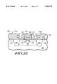
- FIGS. 1-7 illustrate a metal gate MOS process used for forming a semiconductor device 10. Processing begins by providing a semiconductor substrate 12.
- Substrate 12 is preferably a silicon wafer, but may be one or more of a germanium substrate, a gallium arsenide substrate, a germanium-silicon substrate, a silicon on insulator substrate (SOI), epitaxial regions, indium phosphide substrates, other III-V compounds, silicon carbide substrates, or the like.
- Pad oxidation and nitride masking is utilized along with silicon etch processing to form trenches 14 in the substrate 12 of FIG. 1. These isolation trenches 14 are filled with a dielectric material in order to provide field isolation between active areas of the semiconductor device 10.
- LOCOS local oxidation of silicon
- polysilicon buffered LOCOS or other field isolation schemes may be utilized in the embodiments taught herein.
- FIG. 1 illustrates that one or more of a p-well and/or an n-well is formed in the substrate wherein, for simplicity of illustration, FIG. 1 illustrates only a single well region 16.
- silicide region 18 is one of either cobalt silicide (CoSi 2 ) or nickel silicide (NiSi 2 ) since these two silicide materials are superior materials when used for out-diffusing dopant atoms to form silicon PN junctions.
- CoSi 2 cobalt silicide
- NiSi 2 nickel silicide
- titanium silicide or other known silicides may be used for form the region 18 in FIG. 1.
- the thickness of silicide layer 18 is roughly 300-400 angstroms.
- a double masking step and double ion implant process into different regions of the layer 18 is utilized to form both p-doped regions and an n-doped regions of layer 18. If only n-channel or p-channel transistors are formed on one IC, then insitu doping of the silicide layer 18 may be performed with one of either n-type impurities or p-type impurities.
- donor atoms such as phosphorus, arsenic, and/or antimony are ion implanted into the silicide layer 18.
- acceptor atoms such as boron, BF 2 , and/or indium are ion implanted into the silicide layer 18.
- LDD lightly doped drain
- various regions of the silicide layer 18 may be implanted with two species, such as phosphorous and arsenic. This two-species doping will enable out-diffusion of both highly doped drain regions and lightly doped drain regions within the same thermal process due to differences in coefficients of diffusion for different dopant atoms.
- p-channel active areas in n-type wells contain a layer 18 that is ion implanted with p-type impurities (e.g., boron)
- an n-channel active areas within p-wells contain a layer 18 that is implanted with n-type impurities.
- a substantial portion of the ion implant dopant dose should be contained within the silicide region 18 (e.g., the energy and does should be set so that not much dopants, if any, penetrates through the silicide to the underlying substrate).
- ion implant beam energies between roughly 5 KeV and 30 KeV may be used to achieve this purpose.
- FIG. 2 illustrates that a thin plasma-enhanced nitride (PEN or like material) layer 20 is deposited overlying the trench isolation regions 14 and the silicide layer 18.
- the plasma enhanced nitride layer is deposited to a thickness of roughly 500 angstroms.
- Plasma enhanced nitride layer 20 is provided for use as an etch stop layer when subsequently forming contact openings to source and drain electrodes of the MOS transistors. This etch stop therefore prevents over-etching of contact openings which could damage silicon/silicide contact regions.
- An oxide layer 22 is then deposited overlying a top portion of the plasma-enhanced nitride layer 20.
- the oxide 22 is preferably a low temperature oxide (LTO) due to the presence of the silicide layer 18. Furthermore, a low temperature oxide (LTO) layer 22 is preferred since a low temperature oxide will not result in substantial out diffusion of the dopant atoms contained within the doped silicide layer 18. Typically, the oxide layer 22 is deposited to a final thickness of roughly 1,000-4,000 angstroms with roughly 2,000 angstroms being preferred. In another form, the layer 22 may be formed as a tetraethylorthosilicate (TEOS) layer or an ozone TEOS layer either alone or in combination with another material to form a composite dielectric 22.
- TEOS tetraethylorthosilicate
- a photoresist mask (not specifically illustrated in FIG. 3) is deposited and developed over a top of the oxide layer 22.
- the photoresist mask is processed to form an opening 24.
- This opening 24 is extended into the oxide layer 22 to form an opening 24 through the oxide layer 22 via an oxide etch process.
- this etch is performed using a CF 4 , Chlorine, and/or CHF 3 plasma reactive ion etch (RIE) environments.
- RIE plasma reactive ion etch
- the oxide etch utilized to form the opening 24 will preferably use the plasma enhanced nitride (PEN) layer 20 as an etch stop.
- PEN plasma enhanced nitride
- the exposed portion of the plasma enhanced nitride 20 within the opening 24 is removed by using a silicon nitride etch.
- an NF 3 plasma etch environment is used to reactive ion etch (RIE) exposed portions of the plasma enhanced nitride layer 20 within the opening 24.
- RIE reactive ion etch
- an exposed portion of the silicide layer 18 within the opening 24 is etched away.
- a brief wet etch ambient is used to remove exposed portions of the silicide region 18 in the opening 24.
- piranha may be utilized to remove the exposed portions of the layer 18.
- other wet etch technology and/or a dry etch process may be utilized to perform the etching of exposed portions of layer 18.
- the photoresist mask layer(not specifically illustrated in FIG. 3) is removed and an opening 24 remains in the structure 10.
- the opening 24 exposes a portion of the well region 16 as shown in FIG. 3. It is important to note that the opening 24 has now segmented the layer 18 into two different physically-separated portions. A left portion of layer 18 in FIG. 3 will be utilized to form one source/drain electrode whereas a right portion of layer 18 in FIG. 3 will be utilized to form the other source/drain electrode for a same MOS transistor. These two source and drain electrodes are electrically disconnected by the opening in a preferred form, but may be connected if a MOS capacitor structures (e.g., a two terminal, and not a three terminal, device) is all that is desired.
- a MOS capacitor structures e.g., a two terminal, and not a three terminal, device
- FIG. 4 illustrates that a thermal drive process is utilized to drive the dopant atoms out of the two silicide regions 18 in FIG. 4 to form respective source and drain electrodes 26 and 28 within single crystalline silicon areas.
- This drive process is typically performed at a temperature between 800° C. and 1000° C. for roughly 30 to 90 seconds. Notice that the source and drain electrodes 26 and 28 are formed fully self-aligned to the opening 24 of FIG. 4 since the opening defines the placement of the silicide region 18.
- the regions 26 and 28 are typically driven downward to 1,500-2,000 angstroms in depth and will laterally diffuse roughly 1,000 to 1,500 angstroms in distance.
- a doping concentration of the regions 26 and 28 tends to be on the order of n ⁇ 10 19 to m ⁇ 10 20 dopant atoms per centimeters cubed where n and m are any real numbers.
- the silicide regions 18 remain as a portion of the source and drain electrodes whereby a conductivity of these silicon source/drain electrodes is improved.
- FIG. 5 illustrates that a sacrificial oxide 25 is thermally grown over a substrate surface which is exposed by the opening 24.
- the sacrificial thermal oxide 25 is typically grown to a thickness of roughly 100 angstroms.
- silicon nitride is deposited and reactive ion etched to form silicon nitride spacers 23 on top of the sacrificial oxide 25.
- the etch used to form silicon nitride spacers 23 is selective to the sacrificial oxide 25.
- a threshold (Vt) adjust implant is performed at a low ion implant energy in order to form threshold adjust doped region 31 within the well region 16.
- Punchthrough avoidance ion implants may also be performed at this time.
- an oxide etch is utilized to remove portions of the sacrificial oxide 25 which lie within an inner periphery of the spacer 23. Notice that the spacers 23 provides a necessary offset not only to compensate for lateral diffusion of the source and drain regions 26 and 28, but to electrically isolate subsequent gate electrode formations from the silicide regions 18 whereby Miller effects may be reduced. While nitride spacers formed by deposition may be replaced or composited with a sidewall thermal growth, some silicides do not oxidize effectively and may at least some deposition process to obtain adequate source/drain to gate isolation.
- thermal gate oxidation to form a thermal gate oxide 27 is performed.
- the oxide 27 may be formed as a composite dielectric consisting of a thermally grown layer and a deposited oxide layer which may be optionally nitrided and/or fluorinated.
- the composite-deposited oxide portion may be replaced with a deposited nitride layer and/or a high-k dielectric material such as a metal oxide.
- a metal deposition process is utilized to form a metal layer 28a in FIG. 6.
- layer 28a is made of one or more of molybdenum (Mo), tungsten (W), tungsten silicide (WSi 2 ), nickel silicide (NiSi 2 ), titanium nitride (TiN), composites thereof, or like materials.
- Mo molybdenum
- W tungsten
- WSi 2 tungsten silicide
- NiSi 2 nickel silicide
- TiN titanium nitride
- the thickness of layer 28a should be thick enough to adequately fill the opening 24 of FIG. 5.
- FIG. 7 illustrates that a chemical mechanical polish (CMP) process, a resist etch-back (REB), and/or a blanket etch-back process is used to remove an upper portion of layer 28a.
- CMP chemical mechanical polish
- REB resist etch-back
- FIG. 7 illustrates that a chemical mechanical polish (CMP) process, a resist etch-back (REB), and/or a blanket etch-back process is used to remove an upper portion of layer 28a.
- CMP chemical mechanical polishing
- planarization process of FIG. 7 results in the formation of a metal plug 28b by removing top portions of the layer 28a.
- This metal plug 28b substantially or entirely fills the opening 24 illustrated in FIG. 5.
- the metal region 28b functions as a metallic gate electrode for the semiconductor device 10. It is important to note that the metal electrode 28b is self-aligned to the source and drain electrodes 26 and 28 illustrated in FIG. 7 by virtue of being formed within the self-aligning opening 24.
- a photoresist mask and oxide/plasma enhanced nitride etch process is utilized to subsequently form source and drain contacts to the source and drains of FIG. 7 (not specifically illustrated).
- These source/drain contacts may be formed after metal gate formation or may be formed concurrent with the metal gate formation whereby the source/drain contacts are made of the same material as the metallic gate in an inlaid or dual inlaid manner (see FIGS. 8-9).
- the metal material 28b is preferably a material having a mid-gap work function wherein the threshold voltages (V t ) of both p-type and n-type transistors on the same substrate are compatible. Furthermore, due to the presence of a metal gate, the threshold adjust region 31 may either be avoided or reduced in doping concentration whereby high mobilities through the channel regions can be achieved.
- the metallic gate electrode 28b has a higher conductivity than conventional polysilicon gate electrodes. Furthermore, the metallic electrode 28b of FIG. 7 will not suffer from polysilicon depletion whereby the effective thickness of the oxide 27 is not adversely affected.
- the metal gate 28b allows the gate oxide 27 to be formed as a tantalum pentoxide (Ta 2 O 5 ) layer, titanium oxide (TiO 2 ) layer, other high-k dielectrics, or composites thereof which is not easily integrated into a process flow which uses polysilicon gate electrodes.
- the substrate 12 of FIG. 7 may be provided as a silicon on insulator (SOI) substrate whereby the control of threshold voltages can be accurately achieved using the metallic gate 28b taught herein.
- SOI silicon on insulator
- the metal gate 28b in the process of FIGS. 1-7 need not be exposed to any high temperature processing whereby the metal gate will not be substantially damaged. Even though films, such as tungsten (W) and molybdenum (Mo), cannot adequately block ion implantation of source and drain atoms, this ion implantation blocking property of the gate electrode is not needed when utilizing the self-aligned process taught herein (i.e., the source and drain electrodes in FIGS. 1-7 need no gate electrode ion implant blocking properties in order to be properly formed). Furthermore, metallic adhesion of the metal gate 28b to surrounding oxides is improved over prior art devices, and no difficult metallic etch processing is needed in the device of FIG. 7. Also, the structure of FIG. 7 will avoid or significantly reduce any metal-to-gate-oxide interaction which could substantially degrade MOS transistor performance. These advantages are also present in the other embodiments taught herein in FIGS. 8-18.
- FIGS. 8-9 illustrate a method which may be utilized to form a metal gate MOS transistor utilizing dual inlaid interconnect structures.
- FIG. 8 illustrates a semiconductor device 11 having regions 12-26 which are identical or substantially similar to similarly numbered elements in FIGS. 1-7. Due to the similarities of these elements to previously-discussed elements, these elements 12-26 in FIGS. 8-18 are not further discussed hereinbelow.
- FIG. 8 illustrates that a plasma enhanced nitride (PEN) or like etch stop layer 30 is formed overlying the low temperature oxide (LTO) 22 previously taught. Another low temperature oxide or TEOS layer 32 is then deposited overlying the etch stop layer 30.
- PEN plasma enhanced nitride
- LTO low temperature oxide
- Another low temperature oxide or TEOS layer 32 is then deposited overlying the etch stop layer 30.
- a first photoresist mask (not specifically illustrated in FIG. 8) is used to form an opening 34 through the layer 32. This opening 34 is then extended through exposed portions of the etch stop 30 using a second plasma etch environment.
- the etch of layer 32 is preferably performed selective to the etch stop layer 30, and the etch of layer 30 is preferentially performed substantially selective to layer 22.
- a width dimension X of the opening 34 through the layers 32 and 30 is illustrated in FIG. 8.
- the photoresist used to form X is removed and a photoresist having the dimension Y is formed and the openings 36 (in layer 32) and the deepening of the layer 34 (into layer 22) are performed together in FIG. 9.
- FIG. 7 may be used to etch through the layer 30 and 22 to fully deepen the opening 34 through the layer 22 before patterning the photoresist to the dimension Y.
- a "via first" inlaid trench process is shown in the embodiment of FIGS. 8-9.
- the photoresist layer used to pattern 34 is stripped from the surface of structure 11 and a second photoresist mask is utilized to define a second opening having a width dimension Y as illustrated in FIG. 8.
- FIG. 9 illustrates that the photoresist mask which contains the opening dimension Y is utilized to etch a wider opening having a dimension Y through the layers 32 and 30 above the opening having the dimension X.
- the opening 34 is either previously etched as discussed with respect to FIG. 8 through layer 22 or is now deepened to penetrate through the layer 22 and expose the plasma enhanced nitride (PEN) layer 20.
- PEN plasma enhanced nitride
- a nitride etch is then utilized to remove portions of the nitride layer 20 and the nitride layer 30 which are exposed within the dual inlaid openings. It is important to note that the etch used to from the gate opening X in FIG.
- the dual inlaid gate 34 of FIG. 9 may be coupled to another gate and/or one or more source and drain electrodes of another device on the IC via the interconnect portion 36 of FIG. 9.
- a wet silicide etch process is utilized to remove exposed portions of the region 18 to result in segmented source and drain regions as previously discussed for FIGS. 1-7. Note that the silicide/salicide regions of any exposed source and drain contacts are protected by photoresist during this gate-hole silicide strip operation (not shown ion FIG. 9) to remove silicide in channel region but maintain silicide in exposed source/drain regions.
- sacrificial gate oxide processing and sidewall spacers 38 and 40 are performed. Spacers 38 and 40 are formed by depositing a conformal layer of silicon nitride and reactive ion etching (RIE) the layer to form both the spacers 38 and 40 simultaneously.
- RIE reactive ion etching
- a gate oxide 27 is thermally grown. A deposited gate oxide 27 may be used to form a composite gate dielectric, however, this composite formation may require that a second masking operation and oxide etch process be utilized to clear exposed silicide source and drain regions to which the dual inlaid interconnect is to couple.
- a metallic material is then chemically mechanically polished (CMP) or etched back to result in a metallic plug 36.
- CMP chemically mechanically polished
- a lower portion of the metallic region within region 34 functions as a gate electrode for a transistor or functions as a capacitor electrode for a capacitor.
- a top portion of the metallic plug 36 functions as a local interconnect which couples the lower metallic electrode within opening 34 to another active device on the integrated circuit (IC).
- This metallic interconnect dual inlaid structure has a lower resistance than conventional polysilicon interconnects.
- FIGS. 10-18 illustrate another embodiment for forming a metal gate MOS transistor in a self-aligned manner.
- FIG. 10 illustrates a semiconductor device 100 having a substrate 102. Trench isolation regions 104 are formed as discussed herein with respect to FIG. 1. Doped well regions 103 (at least one of n-type well regions or p-type well regions) are also formed to enable CMOS device formation as is discussed herein. A sacrificial thermal gate oxide 105 is formed in FIG. 10 and subsequently removed to clean an active surface within the well regions 103.
- FIG. 11 illustrates that a gate oxide 106 is formed after removal of the sacrificial oxide 105.
- a polysilicon layer 108 is formed over the gate dielectric 106.
- An anti-reflective coating (ARC) layer 110 is formed overlying the polysilicon layer 108.
- a photoresist mask (not specifically illustrated in FIG. 11) is spun on the semiconductor wafer and developed in order to etch a gate stack from the layers 106 through 110 as illustrated in FIG. 11.
- FIG. 12 illustrates that a gate sidewall oxidation 112 is performed.
- silicon nitride spacers 114 are formed laterally adjacent the gate stack in FIG. 12.
- Conventional source and drain ion implantation and lightly doped drain (LDD) processing is then utilized in FIG. 12 to form source and drain electrodes 118 in a self-aligned manner.
- LDD lightly doped drain
- FIG. 13 illustrates that a refractory metal layer is deposited over the wafer.
- a thermal process is initiated to react the refractory metal with the exposed silicon source and drain regions to form an upper silicide layer 116 as a portion of the source and drain regions.
- This silicide layer 116 is preferably cobalt silicide or titanium silicide.
- a silicide layer is not formed on top of the polysilicon layer due to the presence of the anti-reflective coating 110.
- FIG. 14 illustrates that a plasma enhanced nitride (PEN) layer 120 is formed overlying the semiconductor device 100.
- a TEOS layer 122 is formed.
- LTO low temperature oxide
- BPSG borophosphosilicate glass
- FIG. 15 a chemical mechanical polish (CMP) process is used wherein the chemical mechanical polish uses the polysilicon layer 108 as a polish stop. This chemical mechanical polishing (CMP) process will therefore expose a top surface of the polysilicon layer 108 as illustrated in FIG. 15.
- CMP chemical mechanical polish
- FIG. 16 illustrates that a plasma reactive ion etch (RIE) using chlorine or a wet polysilicon etch using conventional etch chemistry is utilized to remove the polysilicon layer 110 to form a feature opening 124.
- An ion implantation threshold (Vt) adjust implant and/or a punchthrough adjust ion implant is then optionally performed as needed through the feature 124 and the gate oxide 106 to form a threshold voltage doped region 126.
- thermal oxide is used for sacrificial layer 106.
- any layer or composite which acts as an etch stop for polysilicon removal can be used.
- Oxide 106 is typically a sacrificial oxide which is removed and replaced with a gate oxide 125 which is either thermal silicon dioxide or of like composition to layer 106.
- layer 106 may comprise all or part of the final gate dielectric layer 125. High-k layers may also be used to form the dielectric layers 125 and 106.
- FIG. 17 illustrates that a metal deposition or sputtering process is utilized to form a layer of metal 128a which fills the feature size 124.
- the metal material is preferably tungsten, molybdenum, titanium nitride, tungsten silicide, titanium silicide, like conductive layers, or composites thereof.
- FIG. 18 illustrates that the metal layer 128a is chemical mechanical polished (CMP) to form a metal plug region 128b within the feature opening 124. It is important to note that the metal gate 128b is of a substantially similar dimension and location as the polysilicon gate 108 of FIG. 11. Therefore, the metal gate 128b is self-aligned to the source and drain regions 118 formed within the substrate as was the temporary polysilicon dummy gate region 108 of FIG. 12. Therefore, FIG. 18 illustrates the formation of a metal gate MOS transistor having all of the advantages discussed herein.
- CMP chemical mechanical polished
- FIGS. 19-22 illustrate another embodiment for forming a self-aligned MOS transistor and a metallic interconnect layer in the same dielectric material.
- FIGS. 10-16 illustrate the formation of the substrate with the sacrificial gate material removed.
- FIG. 19 illustrates that a metal deposition or sputtering process is utilized to form a thin layer of metal 129 which fills the feature size 124.
- the metal material is preferably tungsten, molybdenum, titanium nitride (TiN), tungsten silicide, titanium silicide, like conductive layers, or composites thereof.
- a photoresist mask (not specifically illustrated in FIG. 20) is spun on the semiconductor wafer and developed in order to etch an interconnect feature 130 through the layers 129, 122 and 120.
- the layer 129 may be polished in FIG. 20 before the openings are formed in FIG. 20.
- the etch of the openings in FIG. 20 stops on substrate 102 and may etch a small portion of the trench region 104.
- FIG. 21 illustrates that a metal deposition or sputtering process is utilized to form a layer of metal 131a which fills the feature size 124 and 130.
- the metal material is preferably tungsten, molybdenum, titanium nitride, tungsten silicide, titanium silicide, like conductive layers, or composites thereof.
- FIG. 22 illustrates that the metal layer 131a is chemical mechanical polished (CMP) to form a metal plug region 131b within the feature opening 124 and metal plug region 131c within the feature opening 130.
- CMP chemical mechanical polished
- the metal gate 131b is of a substantially similar dimension and location as the polysilicon gate 108 of FIG. 11. Therefore, the metal gate 131b is self-aligned to the source and drain regions 118 formed within the substrate as was the temporary polysilicon dummy gate region 108 of FIG. 12. Therefore, FIG. 22 illustrates the formation of a metal gate MOS transistor having all of the advantages discussed herein. Further, FIG. 22 illustrates the formation of a metallic interconnect having all the advantages discussed herein.
- metallic layers 129 and 131a may be polished in the same processing in FIG. 22 or may be polished separately (layer 129 being polished in FIG. 20 to form a first plug and layer 131a polished with a second CMP process in FIG. 22 to complete the plug structure.
- regions 131b and 131c are coupled to other source and drain regions or other gate electrodes off-the-page of FIG. 22 by etching away the regions
Abstract
Description
Claims (43)
Priority Applications (1)
| Application Number | Priority Date | Filing Date | Title |
|---|---|---|---|
| US08/907,990 US5960270A (en) | 1997-08-11 | 1997-08-11 | Method for forming an MOS transistor having a metallic gate electrode that is formed after the formation of self-aligned source and drain regions |
Applications Claiming Priority (1)
| Application Number | Priority Date | Filing Date | Title |
|---|---|---|---|
| US08/907,990 US5960270A (en) | 1997-08-11 | 1997-08-11 | Method for forming an MOS transistor having a metallic gate electrode that is formed after the formation of self-aligned source and drain regions |
Publications (1)
| Publication Number | Publication Date |
|---|---|
| US5960270A true US5960270A (en) | 1999-09-28 |
Family
ID=25424983
Family Applications (1)
| Application Number | Title | Priority Date | Filing Date |
|---|---|---|---|
| US08/907,990 Expired - Lifetime US5960270A (en) | 1997-08-11 | 1997-08-11 | Method for forming an MOS transistor having a metallic gate electrode that is formed after the formation of self-aligned source and drain regions |
Country Status (1)
| Country | Link |
|---|---|
| US (1) | US5960270A (en) |
Cited By (245)
| Publication number | Priority date | Publication date | Assignee | Title |
|---|---|---|---|---|
| US6033963A (en) * | 1999-08-30 | 2000-03-07 | Taiwan Semiconductor Manufacturing Company | Method of forming a metal gate for CMOS devices using a replacement gate process |
| US6066533A (en) * | 1998-09-29 | 2000-05-23 | Advanced Micro Devices, Inc. | MOS transistor with dual metal gate structure |
| US6087231A (en) * | 1999-08-05 | 2000-07-11 | Advanced Micro Devices, Inc. | Fabrication of dual gates of field transistors with prevention of reaction between the gate electrode and the gate dielectric with a high dielectric constant |
| US6090672A (en) * | 1998-07-22 | 2000-07-18 | Wanlass; Frank M. | Ultra short channel damascene MOS transistors |
| US6093590A (en) * | 1999-09-14 | 2000-07-25 | Worldwide Semiconductor Manufacturing Corp. | Method of fabricating transistor having a metal gate and a gate dielectric layer with a high dielectric constant |
| US6096641A (en) * | 1999-01-19 | 2000-08-01 | Mitsubishi Denki Kabushiki Kaisha | Method of manufacturing semiconductor device |
| US6114206A (en) * | 1998-11-06 | 2000-09-05 | Advanced Micro Devices, Inc. | Multiple threshold voltage transistor implemented by a damascene process |
| US6117741A (en) * | 1998-01-09 | 2000-09-12 | Texas Instruments Incorporated | Method of forming a transistor having an improved sidewall gate structure |
| US6124188A (en) * | 1998-12-01 | 2000-09-26 | Advanced Micro Devices, Inc. | Semiconductor device and fabrication method using a germanium sacrificial gate electrode plug |
| US6127258A (en) * | 1998-06-25 | 2000-10-03 | Motorola Inc. | Method for forming a semiconductor device |
| US6133128A (en) * | 1997-12-30 | 2000-10-17 | Intel Corporation | Method for patterning polysilicon gate layer based on a photodefinable hard mask process |
| US6140167A (en) * | 1998-08-18 | 2000-10-31 | Advanced Micro Devices, Inc. | High performance MOSFET and method of forming the same using silicidation and junction implantation prior to gate formation |
| US6143593A (en) * | 1998-09-29 | 2000-11-07 | Conexant Systems, Inc. | Elevated channel MOSFET |
| US6150241A (en) * | 1996-06-27 | 2000-11-21 | Commissariat A L'energie Atomique | Method for producing a transistor with self-aligned contacts and field insulation |
| US6165883A (en) * | 1998-11-20 | 2000-12-26 | Kabushiki Kaisha Toshiba | Method for forming multilayer sidewalls on a polymetal stack gate electrode |
| US6169006B1 (en) * | 1998-07-29 | 2001-01-02 | Advanced Micro Devices, Inc. | Semiconductor device having grown oxide spacers and method of manufacture thereof |
| US6171921B1 (en) * | 1998-06-05 | 2001-01-09 | Motorola, Inc. | Method for forming a thick-film resistor and thick-film resistor formed thereby |
| US6174794B1 (en) * | 1998-08-20 | 2001-01-16 | Advanced Micro Devices, Inc. | Method of making high performance MOSFET with polished gate and source/drain feature |
| US6184114B1 (en) * | 1999-08-17 | 2001-02-06 | Advanced Micro Devices, Inc. | MOS transistor formation |
| US6197642B1 (en) * | 1997-10-18 | 2001-03-06 | United Microelectronics Corp. | Method for manufacturing gate terminal |
| US6214677B1 (en) * | 1999-10-22 | 2001-04-10 | United Microelectronics Corp. | Method of fabricating self-aligned ultra short channel |
| US6214654B1 (en) * | 1999-01-27 | 2001-04-10 | Advanced Micro Devices, Inc. | Method for forming super-steep retrograded channel (SSRC) for CMOS transistor using rapid laser annealing to reduce thermal budget |
| EP1091414A2 (en) * | 1999-10-07 | 2001-04-11 | Lucent Technologies Inc. | MOSFET with tapered gate and method of manufacturing it |
| US6218275B1 (en) * | 1999-05-13 | 2001-04-17 | Mosel Vitelic, Inc. | Process for forming self-aligned contact of semiconductor device |
| US6251763B1 (en) * | 1997-06-30 | 2001-06-26 | Kabushiki Kaisha Toshiba | Semiconductor device and method for manufacturing same |
| US6251760B1 (en) * | 1998-01-19 | 2001-06-26 | Hyundai Electronics Industries Co. Ltd. | Semiconductor device and its wiring and a fabrication method thereof |
| US6262456B1 (en) | 1998-11-06 | 2001-07-17 | Advanced Micro Devices, Inc. | Integrated circuit having transistors with different threshold voltages |
| US6271573B1 (en) * | 1997-11-28 | 2001-08-07 | Kabushiki Kaisha Toshiba | Semiconductor device with gate structure and method of manufacturing the same |
| US6271132B1 (en) * | 1999-05-03 | 2001-08-07 | Advanced Micro Devices, Inc. | Self-aligned source and drain extensions fabricated in a damascene contact and gate process |
| US6274421B1 (en) * | 1998-01-09 | 2001-08-14 | Sharp Laboratories Of America, Inc. | Method of making metal gate sub-micron MOS transistor |
| US6291278B1 (en) * | 1999-05-03 | 2001-09-18 | Advanced Micro Devices, Inc. | Method of forming transistors with self aligned damascene gate contact |
| US6297107B1 (en) | 2000-10-19 | 2001-10-02 | Advanced Micro Devices, Inc. | High dielectric constant materials as gate dielectrics |
| US6297106B1 (en) * | 1999-05-07 | 2001-10-02 | Chartered Semiconductor Manufacturing Ltd. | Transistors with low overlap capacitance |
| US6300203B1 (en) * | 2000-10-05 | 2001-10-09 | Advanced Micro Devices, Inc. | Electrolytic deposition of dielectric precursor materials for use in in-laid gate MOS transistors |
| US6300177B1 (en) | 2001-01-25 | 2001-10-09 | Chartered Semiconductor Manufacturing Inc. | Method to form transistors with multiple threshold voltages (VT) using a combination of different work function gate materials |
| US6303418B1 (en) | 2000-06-30 | 2001-10-16 | Chartered Semiconductor Manufacturing Ltd. | Method of fabricating CMOS devices featuring dual gate structures and a high dielectric constant gate insulator layer |
| US6306741B1 (en) | 2000-07-13 | 2001-10-23 | Chartered Semiconductor Manufacturing, Inc. | Method of patterning gate electrodes with high K gate dielectrics |
| US6316323B1 (en) * | 2000-03-21 | 2001-11-13 | United Microelectronics Corp. | Method for forming bridge free silicide by reverse spacer |
| US6319839B1 (en) * | 1999-10-04 | 2001-11-20 | Taiwan Semiconductor Manufacturing Company | Approach to form an inter-polysilicon oxide (IPO) layer for charge coupled devices |
| US6326251B1 (en) * | 1999-01-12 | 2001-12-04 | Advanced Micro Devices | Method of making salicidation of source and drain regions with metal gate MOSFET |
| US6329232B1 (en) * | 1999-06-30 | 2001-12-11 | Hyundai Electronics Co., Ltd. | Method of manufacturing a semiconductor device |
| US6333223B1 (en) * | 1998-12-25 | 2001-12-25 | Matsushita Electric Industrial Co., Ltd. | Semiconductor device and method of manufacturing the same |
| US6342414B1 (en) * | 2000-12-12 | 2002-01-29 | Advanced Micro Devices, Inc. | Damascene NiSi metal gate high-k transistor |
| US6342441B1 (en) * | 1999-04-02 | 2002-01-29 | Hyundai Electronics Industries Co., Ltd. | Method for fabricating semiconductor device |
| US6346450B1 (en) * | 1996-12-16 | 2002-02-12 | Commissariat A L'energie Atomique | Process for manufacturing MIS transistor with self-aligned metal grid |
| US6362058B1 (en) * | 1999-12-22 | 2002-03-26 | Texas Instruments Incorporated | Method for controlling an implant profile in the channel of a transistor |
| US6368950B1 (en) | 2000-12-12 | 2002-04-09 | Advanced Micro Devices, Inc. | Silicide gate transistors |
| US6376350B1 (en) * | 2001-02-23 | 2002-04-23 | Advanced Micro Devices, Inc. | Method of forming low resistance gate electrode |
| US6383884B1 (en) * | 1999-09-09 | 2002-05-07 | Mitsubishi Denki Kabushiki Kaisha | Method of manufacturing semiconductor device |
| US20020058368A1 (en) * | 2000-11-14 | 2002-05-16 | Horng-Huei Tseng | Method of fabricating a dummy gate electrode of an ESD protecting device |
| US6391727B1 (en) | 1999-12-24 | 2002-05-21 | Hyundai Electronics Industries Co., Ltd. | Method of manufacturing a semiconductor device utilizing a(Al2O3)X-(TiO2)1-X gate dielectric film |
| US6392280B1 (en) | 2000-10-19 | 2002-05-21 | Advanced Micro Devices, Inc. | Metal gate with PVD amorphous silicon layer for CMOS devices and method of making with a replacement gate process |
| US6399431B1 (en) * | 2000-03-21 | 2002-06-04 | Chartered Semiconductor Manufacturing Ltd. | ESD protection device for SOI technology |
| EP1211716A2 (en) * | 2000-12-04 | 2002-06-05 | Sharp Kabushiki Kaisha | Semiconductor device and fabrication process therefor using a dummy gate |
| US6417056B1 (en) * | 2001-10-18 | 2002-07-09 | Chartered Semiconductor Manufacturing Ltd. | Method to form low-overlap-capacitance transistors by forming microtrench at the gate edge |
| EP1227513A2 (en) * | 2001-01-26 | 2002-07-31 | Chartered Semiconductor Manufacturing, Inc. | Method for forming variable-K gate dielectric |
| US6436746B1 (en) * | 1998-01-12 | 2002-08-20 | Texas Instruments Incorporated | Transistor having an improved gate structure and method of construction |
| US6436840B1 (en) | 2000-10-19 | 2002-08-20 | Advanced Micro Devices, Inc. | Metal gate with CVD amorphous silicon layer and a barrier layer for CMOS devices and method of making with a replacement gate process |
| US6440868B1 (en) | 2000-10-19 | 2002-08-27 | Advanced Micro Devices, Inc. | Metal gate with CVD amorphous silicon layer and silicide for CMOS devices and method of making with a replacement gate process |
| US6440867B1 (en) | 2000-10-19 | 2002-08-27 | Advanced Micro Devices, Inc. | Metal gate with PVD amorphous silicon and silicide for CMOS devices and method of making the same with a replacement gate process |
| US6444512B1 (en) * | 2000-06-12 | 2002-09-03 | Motorola, Inc. | Dual metal gate transistors for CMOS process |
| US6448630B1 (en) * | 1998-10-15 | 2002-09-10 | Mitsubishi Denki Kabushiki Kaisha | Semiconductor device comprising a polish preventing pattern |
| US6455383B1 (en) * | 2001-10-25 | 2002-09-24 | Silicon-Based Technology Corp. | Methods of fabricating scaled MOSFETs |
| US6458717B1 (en) | 2000-07-13 | 2002-10-01 | Chartered Semiconductor Manufacturing Ltd. | Methods of forming ultra-thin buffer oxide layers for gate dielectrics |
| US6458639B1 (en) * | 1998-09-02 | 2002-10-01 | Advanced Micro Devices, Inc. | MOS transistor with stepped gate insulator |
| US6461910B1 (en) | 1999-11-09 | 2002-10-08 | Hyundai Electronics Industries Co., Ltd. | Method of forming a capacitor in a semiconductor device |
| US6465309B1 (en) | 2000-12-12 | 2002-10-15 | Advanced Micro Devices, Inc. | Silicide gate transistors |
| US6465334B1 (en) | 2000-10-05 | 2002-10-15 | Advanced Micro Devices, Inc. | Enhanced electroless deposition of dielectric precursor materials for use in in-laid gate MOS transistors |
| FR2823597A1 (en) * | 2001-04-12 | 2002-10-18 | St Microelectronics Sa | MOS transistor production with gate length less than that imposed by photolithography comprises forming internal spacers in cavity arranged in pile before deposition of gate material |
| US6468874B1 (en) | 1999-12-27 | 2002-10-22 | Hyundai Electronic Industries Co., Ltd. | Method of manufacturing a capacitor in a semiconductor device |
| US6476454B2 (en) * | 2000-03-27 | 2002-11-05 | Kabushiki Kaisha Toshiba | Semiconductor device and method of manufacturing the same |
| US6475908B1 (en) | 2001-10-18 | 2002-11-05 | Chartered Semiconductor Manufacturing Ltd. | Dual metal gate process: metals and their silicides |
| US6475874B2 (en) * | 2000-12-07 | 2002-11-05 | Advanced Micro Devices, Inc. | Damascene NiSi metal gate high-k transistor |
| US6475844B1 (en) * | 1999-02-01 | 2002-11-05 | Mitsubishi Denki Kabushiki Kaisha | Field effect transistor and method of manufacturing same |
| US6492249B2 (en) | 1999-05-03 | 2002-12-10 | Advanced Micro Devices, Inc. | High-K gate dielectric process with process with self aligned damascene contact to damascene gate and a low-k inter level dielectric |
| US6495437B1 (en) * | 2001-02-09 | 2002-12-17 | Advanced Micro Devices, Inc. | Low temperature process to locally form high-k gate dielectrics |
| US6498071B2 (en) * | 1999-11-30 | 2002-12-24 | Koninklijke Phillips Electronics N.V. | Manufacture of trench-gate semiconductor devices |
| US6500718B2 (en) | 1999-12-23 | 2002-12-31 | Dongbu Electronics Co., Ltd. | Method for fabricating semiconductor device |
| US6504210B1 (en) * | 2000-06-23 | 2003-01-07 | International Business Machines Corporation | Fully encapsulated damascene gates for Gigabit DRAMs |
| US6511883B1 (en) * | 1999-07-07 | 2003-01-28 | United Microelectronics Corp. | Method of fabricating MOS sensor |
| US6514826B1 (en) | 1999-12-22 | 2003-02-04 | Hyundai Electronics Industries Co., Ltd. | Method of forming a gate electrode in a semiconductor device |
| US6518623B1 (en) | 2000-06-09 | 2003-02-11 | Mitsubishi Denki Kabushiki Kaisha | Semiconductor device having a buried-channel MOS structure |
| US6518113B1 (en) | 2001-02-06 | 2003-02-11 | Advanced Micro Devices, Inc. | Doping of thin amorphous silicon work function control layers of MOS gate electrodes |
| KR100372639B1 (en) * | 2000-06-21 | 2003-02-17 | 주식회사 하이닉스반도체 | Method of manufacturing mosfet device |
| US6524920B1 (en) | 2001-02-09 | 2003-02-25 | Advanced Micro Devices, Inc. | Low temperature process for a transistor with elevated source and drain |
| US6528362B1 (en) | 2000-10-19 | 2003-03-04 | Advanced Micro Devices, Inc. | Metal gate with CVD amorphous silicon layer for CMOS devices and method of making with a replacement gate process |
| WO2003021662A1 (en) * | 2001-08-28 | 2003-03-13 | Advanced Micro Devices, Inc. | Improved high k-dielectrics using nickel silicide |
| US6541320B2 (en) * | 2001-08-10 | 2003-04-01 | International Business Machines Corporation | Method to controllably form notched polysilicon gate structures |
| US6544851B2 (en) * | 2000-02-17 | 2003-04-08 | Koninklijke Philips Electronics N.V. | Method of manufacturing a semiconductor device having a pocket implant in channel region |
| US6544827B2 (en) * | 1998-08-24 | 2003-04-08 | Nec Corporation | Metal-gate field effect transistor and method for manufacturing the same |
| US6555872B1 (en) | 2000-11-22 | 2003-04-29 | Thunderbird Technologies, Inc. | Trench gate fermi-threshold field effect transistors |
| US6559051B1 (en) | 2000-10-05 | 2003-05-06 | Advanced Micro Devices, Inc. | Electroless deposition of dielectric precursor materials for use in in-laid gate MOS transistors |
| US6562721B2 (en) * | 2000-01-26 | 2003-05-13 | Nec Electronics Corporation | Dry etching method and method of manufacturing semiconductor device |
| US6562717B1 (en) * | 2000-10-05 | 2003-05-13 | Advanced Micro Devices, Inc. | Semiconductor device having multiple thickness nickel silicide layers |
| US6586808B1 (en) | 2002-06-06 | 2003-07-01 | Advanced Micro Devices, Inc. | Semiconductor device having multi-work function gate electrode and multi-segment gate dielectric |
| US6589866B1 (en) | 2000-10-19 | 2003-07-08 | Advanced Micro Devices, Inc. | Metal gate with PVD amorphous silicon layer having implanted dopants for CMOS devices and method of making with a replacement gate process |
| KR100390949B1 (en) * | 2001-06-29 | 2003-07-12 | 주식회사 하이닉스반도체 | Method of manufactuing a transistor in a semiconductor device |
| US20030143791A1 (en) * | 2002-01-29 | 2003-07-31 | Samsung Electronics Co., Ltd. | Methods for fabricating MOS transistors with notched gate electrodes |
| US6602781B1 (en) * | 2000-12-12 | 2003-08-05 | Advanced Micro Devices, Inc. | Metal silicide gate transistors |
| US20030148563A1 (en) * | 2000-03-06 | 2003-08-07 | Kabushiki Kaisha Toshiba | Transistor, semiconductor device and manufacturing method of semiconductor device |
| US6607950B2 (en) | 2000-03-30 | 2003-08-19 | Interuniversitair Microelektronic Centrum (Imec) | MIS transistors with a metal gate and high-k dielectric and method of forming |
| KR20030070523A (en) * | 2002-02-25 | 2003-08-30 | 미쓰비시덴키 가부시키가이샤 | Semiconductor device |
| US6620663B1 (en) * | 2001-05-18 | 2003-09-16 | Episil Technologies, Inc. | Self-aligned copper plating/CMP process for RF lateral MOS device |
| US20030181028A1 (en) * | 2002-03-19 | 2003-09-25 | Yeap Geoffrey C-F | Integrated circuit device and method therefor |
| US6630720B1 (en) * | 2001-12-26 | 2003-10-07 | Advanced Micro Devices, Inc. | Asymmetric semiconductor device having dual work function gate and method of fabrication |
| US20030194849A1 (en) * | 2002-04-16 | 2003-10-16 | Johnson F. Scott | Methods for transistors formation using selective gate implantation |
| US6638776B2 (en) * | 2002-02-15 | 2003-10-28 | Lsi Logic Corporation | Thermal characterization compensation |
| US6642590B1 (en) | 2000-10-19 | 2003-11-04 | Advanced Micro Devices, Inc. | Metal gate with PVD amorphous silicon layer and barrier layer for CMOS devices and method of making with a replacement gate process |
| US20030211681A1 (en) * | 2002-02-26 | 2003-11-13 | International Business Machines Corporation | Fully-depleted SOI MOSFETs with low source and drain resistance and minimal overlap capacitance using a recessed channel damascene gate process |
| US6664195B2 (en) * | 2000-10-13 | 2003-12-16 | Hynix Semiconductor, Inc. | Method for forming damascene metal gate |
| US6664154B1 (en) * | 2002-06-28 | 2003-12-16 | Advanced Micro Devices, Inc. | Method of using amorphous carbon film as a sacrificial layer in replacement gate integration processes |
| US6667199B2 (en) | 2001-07-27 | 2003-12-23 | Hitachi, Ltd. | Semiconductor device having a replacement gate type field effect transistor and its manufacturing method |
| US6674121B2 (en) | 2001-12-14 | 2004-01-06 | The Regents Of The University Of California | Method and system for molecular charge storage field effect transistor |
| US20040018689A1 (en) * | 2002-07-25 | 2004-01-29 | Kim Tae W. | Method for fabricating MOS transistors |
| US6686231B1 (en) * | 2002-12-06 | 2004-02-03 | Advanced Micro Devices, Inc. | Damascene gate process with sacrificial oxide in semiconductor devices |
| US6686282B1 (en) | 2003-03-31 | 2004-02-03 | Motorola, Inc. | Plated metal transistor gate and method of formation |
| US20040023478A1 (en) * | 2002-07-31 | 2004-02-05 | Samavedam Srikanth B. | Capped dual metal gate transistors for CMOS process and method for making the same |
| US20040029345A1 (en) * | 2000-06-09 | 2004-02-12 | Simon Deleonibus | Damascene architecture electronics storage and method for making same |
| KR100418923B1 (en) * | 2001-06-27 | 2004-02-14 | 주식회사 하이닉스반도체 | method for fabricating semiconductor device |
| US20040038517A1 (en) * | 2002-08-20 | 2004-02-26 | Kang Sang-Bum | Methods of forming cobalt silicide contact structures including sidewall spacers for electrical isolation and contact structures formed thereby |
| KR20040025801A (en) * | 2002-09-17 | 2004-03-26 | 아남반도체 주식회사 | Method for forming a gate line in a semiconductor damascene structure |
| KR20040025800A (en) * | 2002-09-17 | 2004-03-26 | 아남반도체 주식회사 | Method for forming a gate line in a semiconductor damascene structure |
| KR20040025804A (en) * | 2002-09-17 | 2004-03-26 | 아남반도체 주식회사 | Method for forming a gate line using of semiconductor dual damascene structure |
| US6746900B1 (en) * | 2003-02-19 | 2004-06-08 | Taiwan Semiconductor Manufacturing Co., Ltd. | Method for forming a semiconductor device having high-K gate dielectric material |
| US6753215B2 (en) * | 2000-09-26 | 2004-06-22 | Seiko Epson Corporation | Methods for manufacturing semiconductor devices and semiconductor devices |
| US6756277B1 (en) | 2001-02-09 | 2004-06-29 | Advanced Micro Devices, Inc. | Replacement gate process for transistors having elevated source and drain regions |
| EP1435647A1 (en) * | 2002-12-30 | 2004-07-07 | STMicroelectronics S.r.l. | Method for forming structures self-aligned with each other on a semiconductor substrate |
| US6762102B2 (en) | 2000-09-26 | 2004-07-13 | Seiko Epson Corporation | Methods for manufacturing semiconductor devices and semiconductor devices |
| US6762469B2 (en) | 2002-04-19 | 2004-07-13 | International Business Machines Corporation | High performance CMOS device structure with mid-gap metal gate |
| US6764966B1 (en) | 2002-02-27 | 2004-07-20 | Advanced Micro Devices, Inc. | Spacers with a graded dielectric constant for semiconductor devices having a high-K dielectric |
| US6764912B1 (en) | 2001-08-02 | 2004-07-20 | Advanced Micro Devices, Inc. | Passivation of nitride spacer |
| US20040157383A1 (en) * | 2002-07-26 | 2004-08-12 | Park Jeong Ho | Method for forming short-channel transistors |
| US6784078B2 (en) * | 2000-09-26 | 2004-08-31 | Seiko Epson Corporation | Methods for manufacturing semiconductor devices and semiconductor devices |
| US6787424B1 (en) | 2001-02-09 | 2004-09-07 | Advanced Micro Devices, Inc. | Fully depleted SOI transistor with elevated source and drain |
| US20040217437A1 (en) * | 2003-04-30 | 2004-11-04 | Andrea Franke | Inverted isolation formed with spacers |
| US6815297B1 (en) * | 2002-02-21 | 2004-11-09 | Advanced Micro Devices, Inc. | Ultra-thin fully depleted SOI device and method of fabrication |
| US6855582B1 (en) | 2003-06-12 | 2005-02-15 | Advanced Micro Devices, Inc. | FinFET gate formation using reverse trim and oxide polish |
| US6864164B1 (en) | 2002-12-17 | 2005-03-08 | Advanced Micro Devices, Inc. | Finfet gate formation using reverse trim of dummy gate |
| US6867128B2 (en) * | 2000-06-09 | 2005-03-15 | Commissariat A L'energie Atomique | Method for making an electronic component with self-aligned drain and gate, in damascene architecture |
| US6867084B1 (en) | 2002-10-03 | 2005-03-15 | Taiwan Semiconductor Manufacturing Company, Ltd. | Gate structure and method of forming the gate dielectric with mini-spacer |
| US6872627B2 (en) | 2001-07-16 | 2005-03-29 | Taiwan Semiconductor Manufacturing Company | Selective formation of metal gate for dual gate oxide application |
| US20050070062A1 (en) * | 2003-09-30 | 2005-03-31 | Mark Visokay | MOS transistor gates with doped silicide and methods for making the same |
| US6888198B1 (en) | 2001-06-04 | 2005-05-03 | Advanced Micro Devices, Inc. | Straddled gate FDSOI device |
| US20050095825A1 (en) * | 2003-10-30 | 2005-05-05 | Kabushiki Kaisha Toshiba | Method of manufacturing semiconductor devices |
| US6893910B1 (en) | 2003-06-17 | 2005-05-17 | Advanced Micro Devices, Inc. | One step deposition method for high-k dielectric and metal gate electrode |
| US20050136677A1 (en) * | 2003-12-18 | 2005-06-23 | Brask Justin K. | Method for making a semiconductor device that includes a metal gate electrode |
| US20050142785A1 (en) * | 2003-12-31 | 2005-06-30 | Dongbuanam Semiconductor Inc. | Method of fabricating semiconductor device |
| US6913983B1 (en) * | 1997-07-18 | 2005-07-05 | Infineon Technologies Ag | Integrated circuit arrangement and method for the manufacture thereof |
| US20050148130A1 (en) * | 2003-12-29 | 2005-07-07 | Doczy Mark L. | Method for making a semiconductor device that includes a metal gate electrode |
| US20050145894A1 (en) * | 2003-12-30 | 2005-07-07 | Chau Robert S. | Replacement gate flow facilitating high yield and incorporation of etch stop layers and/or stressed films |
| GB2409932A (en) * | 2004-01-09 | 2005-07-13 | Ibm | Method of forming gate structures for semiconductor devices |
| US20050153530A1 (en) * | 2004-01-09 | 2005-07-14 | International Business Machines Corporation | Fet gate structure with metal gate electrode and silicide contact |
| US20050153492A1 (en) * | 2004-01-12 | 2005-07-14 | Ahmed Shibly S. | Damascene tri-gate FinFET |
| US20050156229A1 (en) * | 2003-12-16 | 2005-07-21 | Yeap Geoffrey C. | Integrated circuit device and method therefor |
| US6943401B1 (en) * | 2003-09-11 | 2005-09-13 | Advanced Micro Devices, Inc. | Flash memory cell with drain and source formed by diffusion of a dopant from a silicide |
| US20060003558A1 (en) * | 2004-06-30 | 2006-01-05 | Dongbuanam Semiconductor Inc. | Method for fabricating semiconductor device and semiconductor device using the same |
| US20060027883A1 (en) * | 1999-05-21 | 2006-02-09 | Renesas Technology Corp. | Semiconductor device and manufacturing method thereof |
| US20060063322A1 (en) * | 2004-09-21 | 2006-03-23 | Ju-Wang Hsu | Transistor with high dielectric constant gate and method for forming the same |
| KR100582370B1 (en) * | 1999-12-17 | 2006-05-23 | 주식회사 하이닉스반도체 | Method for fabricating gate electrode using damascene process |
| US7084018B1 (en) | 2004-05-05 | 2006-08-01 | Advanced Micro Devices, Inc. | Sacrificial oxide for minimizing box undercut in damascene FinFET |
| US20060194399A1 (en) * | 2004-01-08 | 2006-08-31 | Taiwan Semiconductor Manufacturing Company, Ltd. | Silicide Gate Transistors and Method of Manufacture |
| US20060199321A1 (en) * | 2005-03-03 | 2006-09-07 | Agency For Science, Technology And Research | Fully salicided (FUSA) MOSFET structure |
| US20060223295A1 (en) * | 2005-04-01 | 2006-10-05 | Texas Instruments, Incorporated | Nickel silicide including indium and a method of manufacture therefor |
| US20060246641A1 (en) * | 2005-04-29 | 2006-11-02 | Thorsten Kammler | Technique for forming a contact insulation layer with enhanced stress transfer efficiency |
| US20060270140A1 (en) * | 2002-08-23 | 2006-11-30 | Johnson F Scott | Methods for Transistor Formation Using Selective Gate Implantation |
| US20070007560A1 (en) * | 2005-07-07 | 2007-01-11 | Micron Technology, Inc. | Metal-substituted transistor gates |
| US20070020830A1 (en) * | 2005-07-21 | 2007-01-25 | International Business Machines Corporation | IMPROVED CMOS (Complementary Metal Oxide Semiconductor) TECHNOLOGY |
| US20070049022A1 (en) * | 2005-04-01 | 2007-03-01 | Texas Instruments, Incorporated | Nickel alloy silicide including indium and a method of manufacture therefor |
| US20070045676A1 (en) * | 2005-08-31 | 2007-03-01 | Micron Technology, Inc. | Self aligned metal gates on high-k dielectrics |
| US20070048941A1 (en) * | 2005-09-01 | 2007-03-01 | Micron Technology, Inc. | Transistor gate forming methods and transistor structures |
| WO2007037929A2 (en) * | 2005-09-27 | 2007-04-05 | Freescale Semiconductor | Electronic device with a gate electrode having at least two portions and a process for forming the electronic device |
| US20070090455A1 (en) * | 2005-10-26 | 2007-04-26 | Freescale Semiconductor, Inc. | Electronic device including transistor structures with sidewall spacers and a process for forming the electronic device |
| US20070090437A1 (en) * | 2004-08-04 | 2007-04-26 | Samsung Electronics Co., Ltd. | Semiconductor devices including gate patterns for reducing void formation |
| US20070105295A1 (en) * | 2005-11-08 | 2007-05-10 | Dongbuanam Semiconductor Inc. | Method for forming lightly-doped-drain metal-oxide-semiconductor (LDD MOS) device |
| US20070262415A1 (en) * | 2006-05-11 | 2007-11-15 | Casey Smith | Recessed antifuse structures and methods of making the same |
| US20070264771A1 (en) * | 2006-05-11 | 2007-11-15 | Venkatesan Ananthan | Dual work function recessed access device and methods of forming |
| US20070262395A1 (en) * | 2006-05-11 | 2007-11-15 | Gibbons Jasper S | Memory cell access devices and methods of making the same |
| US7312125B1 (en) | 2004-02-05 | 2007-12-25 | Advanced Micro Devices, Inc. | Fully depleted strained semiconductor on insulator transistor and method of making the same |
| US20080164611A1 (en) * | 2007-01-04 | 2008-07-10 | Qimonda Ag | Method for making an integrated circuit having a via hole |
| WO2008118840A2 (en) * | 2007-03-23 | 2008-10-02 | Texas Instruments Incorporated | Method of manufacturing metal silicide contacts |
| US20080272432A1 (en) * | 2007-03-19 | 2008-11-06 | Advanced Micro Devices, Inc. | Accumulation mode mos devices and methods for fabricating the same |
| US7514360B2 (en) | 2004-03-17 | 2009-04-07 | Hong Yu Yu | Thermal robust semiconductor device using HfN as metal gate electrode and the manufacturing process thereof |
| US7569501B2 (en) | 2002-06-14 | 2009-08-04 | Applied Materials, Inc. | ALD metal oxide deposition process using direct oxidation |
| US20090283836A1 (en) * | 2008-05-13 | 2009-11-19 | International Business Machines Corporation | Cmos structure including protective spacers and method of forming thereof |
| US7645710B2 (en) | 2006-03-09 | 2010-01-12 | Applied Materials, Inc. | Method and apparatus for fabricating a high dielectric constant transistor gate using a low energy plasma system |
| US20100025775A1 (en) * | 2008-07-30 | 2010-02-04 | Martin Giles | Replacement spacers for mosfet fringe capacatance reduction and processes of making same |
| US20100044783A1 (en) * | 2008-08-20 | 2010-02-25 | Taiwan Semiconductor Manufacturing Company, Ltd. | Integrated circuit metal gate structure and method of fabrication |
| US7678710B2 (en) | 2006-03-09 | 2010-03-16 | Applied Materials, Inc. | Method and apparatus for fabricating a high dielectric constant transistor gate using a low energy plasma system |
| US7709402B2 (en) | 2006-02-16 | 2010-05-04 | Micron Technology, Inc. | Conductive layers for hafnium silicon oxynitride films |
| US7824986B2 (en) | 2008-11-05 | 2010-11-02 | Micron Technology, Inc. | Methods of forming a plurality of transistor gates, and methods of forming a plurality of transistor gates having at least two different work functions |
| US7837838B2 (en) | 2006-03-09 | 2010-11-23 | Applied Materials, Inc. | Method of fabricating a high dielectric constant transistor gate using a low energy plasma apparatus |
| CN101901762A (en) * | 2009-03-20 | 2010-12-01 | 台湾积体电路制造股份有限公司 | Be used to form the method for metal gate transistor |
| US20100314698A1 (en) * | 2004-06-18 | 2010-12-16 | Taiwan Semiconductor Manufacturing Company, Ltd. | Methods of manufacturing metal-silicide features |
| US7902018B2 (en) | 2006-09-26 | 2011-03-08 | Applied Materials, Inc. | Fluorine plasma treatment of high-k gate stack for defect passivation |
| US20110121318A1 (en) * | 2006-06-29 | 2011-05-26 | Mrinal Kanti Das | Silicon Carbide Switching Devices Including P-Type Channels |
| US20110186915A1 (en) * | 2010-01-29 | 2011-08-04 | Thilo Scheiper | Replacement gate approach based on a reverse offset spacer applied prior to work function metal deposition |
| US20110207282A1 (en) * | 2005-01-20 | 2011-08-25 | Ronald Kakoschke | Methods for Producing a Tunnel Field-Effect Transistor |
| US20110210380A1 (en) * | 2010-02-26 | 2011-09-01 | Thilo Scheiper | Contact bars with reduced fringing capacitance in a semiconductor device |
| CN102347234A (en) * | 2010-07-29 | 2012-02-08 | 中国科学院微电子研究所 | Structure of semiconductor device and manufacturing method thereof |
| US8119210B2 (en) | 2004-05-21 | 2012-02-21 | Applied Materials, Inc. | Formation of a silicon oxynitride layer on a high-k dielectric material |
| WO2012022109A1 (en) * | 2010-08-19 | 2012-02-23 | 中国科学院微电子研究所 | Semiconductor device structure and manufacturing method thereof |
| WO2012022144A1 (en) * | 2010-08-20 | 2012-02-23 | 中国科学院微电子研究所 | Semiconductor device and manufacturing method of its local interconnect structure |
| US20120112249A1 (en) * | 2009-12-04 | 2012-05-10 | Institute of Microelectronics, Chinese Academy of Sciences | High performance semiconductor device and method of fabricating the same |
| CN101930913B (en) * | 2009-06-26 | 2012-05-23 | 中芯国际集成电路制造(上海)有限公司 | Generating method of metal gate electrode |
| CN102637597A (en) * | 2011-02-10 | 2012-08-15 | 上海宏力半导体制造有限公司 | Vertical PNP (precision navigation processor) preparation method |
| CN102655121A (en) * | 2011-03-03 | 2012-09-05 | 中国科学院微电子研究所 | Sacrifice gate removing method and gate stack manufacturing method |
| US8278203B2 (en) | 2010-07-28 | 2012-10-02 | Sandisk Technologies Inc. | Metal control gate formation in non-volatile storage |
| US20120264281A1 (en) * | 2011-04-12 | 2012-10-18 | Taiwan Semiconductor Manufacturing Company, Ltd. | Method of fabricating a plurality of gate structures |
| CN102790053A (en) * | 2011-05-20 | 2012-11-21 | 美国博通公司 | Combined substrate high-k metal gate device and oxide-polysilicon gate device, and process of fabricating same |
| US8329546B2 (en) * | 2010-08-31 | 2012-12-11 | Taiwan Semiconductor Manufacturing Company, Ltd. | Modified profile gate structure for semiconductor device and methods of forming thereof |
| CN101740518B (en) * | 2008-11-20 | 2012-12-19 | 台湾积体电路制造股份有限公司 | Novel method for removing dummy polysilicon in a gate last process |
| US20130017680A1 (en) * | 2011-07-14 | 2013-01-17 | International Business Machines Corporation | Method of improving replacement metal gate fill |
| US20130049109A1 (en) * | 2011-08-22 | 2013-02-28 | Taiwan Semiconductor Manufacturing Company, Ltd. | Metal Gate Structure |
| CN102956450A (en) * | 2011-08-16 | 2013-03-06 | 中芯国际集成电路制造(北京)有限公司 | Method for manufacturing semiconductor devices |
| US8445345B2 (en) * | 2011-09-08 | 2013-05-21 | International Business Machines Corporation | CMOS structure having multiple threshold voltage devices |
| US20130149835A1 (en) * | 2011-12-09 | 2013-06-13 | Samsung Electronics Co., Ltd. | Semiconductor device and method of fabricating the same |
| US8481378B2 (en) * | 2006-08-01 | 2013-07-09 | Stmicroelectronics (Crolles 2) Sas | Effecting selectivity of silicon or silicon-germanium deposition on a silicon or silicon-germanium substrate by doping |
| CN103296083A (en) * | 2012-02-27 | 2013-09-11 | 中国科学院微电子研究所 | Semiconductor field effect transistor and manufacturing method thereof |
| US8546212B2 (en) * | 2011-12-21 | 2013-10-01 | United Microelectronics Corp. | Semiconductor device and fabricating method thereof |
| US20130295734A1 (en) * | 2012-05-04 | 2013-11-07 | Commissariat A L'energie Atomique Et Aux Energies Alternatives | Method for forming gate, source, and drain contacts on a mos transistor |
| US8623721B2 (en) * | 2011-09-08 | 2014-01-07 | Taiwan Semiconductor Manufacturing Company, Ltd. | Silicide formation and associated devices |
| US20140015051A1 (en) * | 2011-12-05 | 2014-01-16 | International Business Machines Corporation | Method of replacing silicon with metal in integrated circuit chip fabrication |
| CN103681270A (en) * | 2012-09-03 | 2014-03-26 | 中芯国际集成电路制造(上海)有限公司 | Metal grid forming method |
| US20140187010A1 (en) * | 2012-12-31 | 2014-07-03 | Texas Instruments Incorporated | Replacement gate process |
| US8952459B2 (en) * | 2010-03-09 | 2015-02-10 | Taiwan Semiconductor Manufacturing Company, Ltd. | Gate structure having lightly doped region |
| US20150072511A1 (en) * | 2013-09-11 | 2015-03-12 | Taiwan Semiconductor Manufacturing Company, Ltd. | Oxidation and Etching Post Metal Gate CMP |
| US8993389B2 (en) | 2013-01-04 | 2015-03-31 | International Business Machines Corporation | Dummy gate interconnect for semiconductor device |
| US20150118835A1 (en) * | 2013-10-25 | 2015-04-30 | United Microelectronics Corp. | Method for manufacturing semiconductor device |
| US9093421B2 (en) * | 2012-06-26 | 2015-07-28 | International Business Machines Corporation | Implementing gate within a gate utilizing replacement metal gate process |
| US9343470B2 (en) * | 2014-08-13 | 2016-05-17 | Cypress Semiconductor Corporation | Integration of semiconductor memory cells and logic cells |
| US9478623B2 (en) | 2011-08-22 | 2016-10-25 | Taiwan Semiconductor Manufacturing Company, Ltd. | Metal gate structure |
| US20170170289A1 (en) * | 2015-12-11 | 2017-06-15 | Imec Vzw | Transistor device with reduced hot carrier injection effect |
| US20170179123A1 (en) * | 2015-05-15 | 2017-06-22 | Taiwan Semiconductor Manfactuning Company, Ltd. | Fin Field Effect Transistor (FinFET) Device Structure with Uneven Gate Structure |
| US9711411B2 (en) * | 2015-11-10 | 2017-07-18 | United Microelectronics Corp. | Semiconductor device and method for fabricating the same |
| US9966432B2 (en) | 2010-10-07 | 2018-05-08 | Samsung Electronics Co., Ltd. | Semiconductor devices including an etch stop pattern and a sacrificial pattern with coplanar upper surfaces and a gate and a gap fill pattern with coplanar upper surfaces |
| US20180166576A1 (en) * | 2016-12-14 | 2018-06-14 | Taiwan Semiconductor Manufacturing Co., Ltd. | Semiconductor device and method of forming doped channel thereof |
| US10340349B2 (en) | 2015-10-02 | 2019-07-02 | United Microelectronics Corp. | Method of forming semiconductor structure |
| US20190206692A1 (en) * | 2017-01-27 | 2019-07-04 | International Business Machines Corporation | Salicide bottom contacts |
| US10553486B1 (en) | 2018-07-27 | 2020-02-04 | Globalfoundries Inc. | Field effect transistors with self-aligned metal plugs and methods |
| US10777637B2 (en) * | 2019-01-24 | 2020-09-15 | Globalfoundries Inc. | Integrated circuit product with a multi-layer single diffusion break and methods of making such products |
| US11101367B2 (en) | 2015-06-19 | 2021-08-24 | International Business Machines Corporation | Contact-first field-effect transistors |
| US20210328058A1 (en) * | 2015-07-24 | 2021-10-21 | Taiwan Semiconductor Manufacturing Company, Ltd. | Semiconductor device and manufacturing method thereof |
| US11211471B1 (en) | 2020-09-10 | 2021-12-28 | United Microelectronics Corp. | Method of manufacturing a semiconductor device |
| US11245039B2 (en) * | 2015-01-26 | 2022-02-08 | Semiconductor Energy Laboratory Co., Ltd. | Semiconductor device and manufacturing method thereof |
| WO2023092477A1 (en) * | 2021-11-26 | 2023-06-01 | 华为技术有限公司 | Method for preparing transistor, and chip and terminal |
Citations (5)
| Publication number | Priority date | Publication date | Assignee | Title |
|---|---|---|---|---|
| US5391510A (en) * | 1992-02-28 | 1995-02-21 | International Business Machines Corporation | Formation of self-aligned metal gate FETs using a benignant removable gate material during high temperature steps |
| US5393681A (en) * | 1992-09-02 | 1995-02-28 | Motorola, Inc. | Method for forming a compact transistor structure |
| US5434093A (en) * | 1994-08-10 | 1995-07-18 | Intel Corporation | Inverted spacer transistor |
| US5447874A (en) * | 1994-07-29 | 1995-09-05 | Grivna; Gordon | Method for making a semiconductor device comprising a dual metal gate using a chemical mechanical polish |
| US5716861A (en) * | 1991-06-26 | 1998-02-10 | Texas Instruments Incorporated | Insulated-gate field-effect transistor structure and method |
-
1997
- 1997-08-11 US US08/907,990 patent/US5960270A/en not_active Expired - Lifetime
Patent Citations (5)
| Publication number | Priority date | Publication date | Assignee | Title |
|---|---|---|---|---|
| US5716861A (en) * | 1991-06-26 | 1998-02-10 | Texas Instruments Incorporated | Insulated-gate field-effect transistor structure and method |
| US5391510A (en) * | 1992-02-28 | 1995-02-21 | International Business Machines Corporation | Formation of self-aligned metal gate FETs using a benignant removable gate material during high temperature steps |
| US5393681A (en) * | 1992-09-02 | 1995-02-28 | Motorola, Inc. | Method for forming a compact transistor structure |
| US5447874A (en) * | 1994-07-29 | 1995-09-05 | Grivna; Gordon | Method for making a semiconductor device comprising a dual metal gate using a chemical mechanical polish |
| US5434093A (en) * | 1994-08-10 | 1995-07-18 | Intel Corporation | Inverted spacer transistor |
Cited By (394)
| Publication number | Priority date | Publication date | Assignee | Title |
|---|---|---|---|---|
| US6150241A (en) * | 1996-06-27 | 2000-11-21 | Commissariat A L'energie Atomique | Method for producing a transistor with self-aligned contacts and field insulation |
| US6346450B1 (en) * | 1996-12-16 | 2002-02-12 | Commissariat A L'energie Atomique | Process for manufacturing MIS transistor with self-aligned metal grid |
| US6251763B1 (en) * | 1997-06-30 | 2001-06-26 | Kabushiki Kaisha Toshiba | Semiconductor device and method for manufacturing same |
| US6913983B1 (en) * | 1997-07-18 | 2005-07-05 | Infineon Technologies Ag | Integrated circuit arrangement and method for the manufacture thereof |
| US6197642B1 (en) * | 1997-10-18 | 2001-03-06 | United Microelectronics Corp. | Method for manufacturing gate terminal |
| US6271573B1 (en) * | 1997-11-28 | 2001-08-07 | Kabushiki Kaisha Toshiba | Semiconductor device with gate structure and method of manufacturing the same |
| US6207541B1 (en) * | 1997-12-30 | 2001-03-27 | Intel Corporation | Method employing silicon nitride spacers for making an integrated circuit device |
| US6133128A (en) * | 1997-12-30 | 2000-10-17 | Intel Corporation | Method for patterning polysilicon gate layer based on a photodefinable hard mask process |
| US6274421B1 (en) * | 1998-01-09 | 2001-08-14 | Sharp Laboratories Of America, Inc. | Method of making metal gate sub-micron MOS transistor |
| US6117741A (en) * | 1998-01-09 | 2000-09-12 | Texas Instruments Incorporated | Method of forming a transistor having an improved sidewall gate structure |
| US6753559B2 (en) * | 1998-01-12 | 2004-06-22 | Texas Instruments Incorporated | Transistor having improved gate structure |
| US6436746B1 (en) * | 1998-01-12 | 2002-08-20 | Texas Instruments Incorporated | Transistor having an improved gate structure and method of construction |
| US6251760B1 (en) * | 1998-01-19 | 2001-06-26 | Hyundai Electronics Industries Co. Ltd. | Semiconductor device and its wiring and a fabrication method thereof |
| US6229098B1 (en) | 1998-06-05 | 2001-05-08 | Motorola, Inc. | Method for forming a thick-film resistor and thick-film resistor formed thereby |
| US6171921B1 (en) * | 1998-06-05 | 2001-01-09 | Motorola, Inc. | Method for forming a thick-film resistor and thick-film resistor formed thereby |
| US6127258A (en) * | 1998-06-25 | 2000-10-03 | Motorola Inc. | Method for forming a semiconductor device |
| US6372665B1 (en) | 1998-06-25 | 2002-04-16 | Motorola Inc. | Method for forming a semiconductor device |
| US6090672A (en) * | 1998-07-22 | 2000-07-18 | Wanlass; Frank M. | Ultra short channel damascene MOS transistors |
| US6169006B1 (en) * | 1998-07-29 | 2001-01-02 | Advanced Micro Devices, Inc. | Semiconductor device having grown oxide spacers and method of manufacture thereof |
| US6140167A (en) * | 1998-08-18 | 2000-10-31 | Advanced Micro Devices, Inc. | High performance MOSFET and method of forming the same using silicidation and junction implantation prior to gate formation |
| US6174794B1 (en) * | 1998-08-20 | 2001-01-16 | Advanced Micro Devices, Inc. | Method of making high performance MOSFET with polished gate and source/drain feature |
| US6544827B2 (en) * | 1998-08-24 | 2003-04-08 | Nec Corporation | Metal-gate field effect transistor and method for manufacturing the same |
| US6458639B1 (en) * | 1998-09-02 | 2002-10-01 | Advanced Micro Devices, Inc. | MOS transistor with stepped gate insulator |
| US6143593A (en) * | 1998-09-29 | 2000-11-07 | Conexant Systems, Inc. | Elevated channel MOSFET |
| US6066533A (en) * | 1998-09-29 | 2000-05-23 | Advanced Micro Devices, Inc. | MOS transistor with dual metal gate structure |
| US6630710B1 (en) | 1998-09-29 | 2003-10-07 | Newport Fab, Llc | Elevated channel MOSFET |
| US6448630B1 (en) * | 1998-10-15 | 2002-09-10 | Mitsubishi Denki Kabushiki Kaisha | Semiconductor device comprising a polish preventing pattern |
| US6114206A (en) * | 1998-11-06 | 2000-09-05 | Advanced Micro Devices, Inc. | Multiple threshold voltage transistor implemented by a damascene process |
| US6262456B1 (en) | 1998-11-06 | 2001-07-17 | Advanced Micro Devices, Inc. | Integrated circuit having transistors with different threshold voltages |
| US6165883A (en) * | 1998-11-20 | 2000-12-26 | Kabushiki Kaisha Toshiba | Method for forming multilayer sidewalls on a polymetal stack gate electrode |
| US6124188A (en) * | 1998-12-01 | 2000-09-26 | Advanced Micro Devices, Inc. | Semiconductor device and fabrication method using a germanium sacrificial gate electrode plug |
| US6509225B2 (en) | 1998-12-25 | 2003-01-21 | Matsushita Electric Industrial Co., Ltd. | Semiconductor device and method of manufacturing the same |
| US6333223B1 (en) * | 1998-12-25 | 2001-12-25 | Matsushita Electric Industrial Co., Ltd. | Semiconductor device and method of manufacturing the same |
| US6326251B1 (en) * | 1999-01-12 | 2001-12-04 | Advanced Micro Devices | Method of making salicidation of source and drain regions with metal gate MOSFET |
| US6096641A (en) * | 1999-01-19 | 2000-08-01 | Mitsubishi Denki Kabushiki Kaisha | Method of manufacturing semiconductor device |
| US6214654B1 (en) * | 1999-01-27 | 2001-04-10 | Advanced Micro Devices, Inc. | Method for forming super-steep retrograded channel (SSRC) for CMOS transistor using rapid laser annealing to reduce thermal budget |
| US6475844B1 (en) * | 1999-02-01 | 2002-11-05 | Mitsubishi Denki Kabushiki Kaisha | Field effect transistor and method of manufacturing same |
| US6342441B1 (en) * | 1999-04-02 | 2002-01-29 | Hyundai Electronics Industries Co., Ltd. | Method for fabricating semiconductor device |
| US6271132B1 (en) * | 1999-05-03 | 2001-08-07 | Advanced Micro Devices, Inc. | Self-aligned source and drain extensions fabricated in a damascene contact and gate process |
| US6492249B2 (en) | 1999-05-03 | 2002-12-10 | Advanced Micro Devices, Inc. | High-K gate dielectric process with process with self aligned damascene contact to damascene gate and a low-k inter level dielectric |
| US6291278B1 (en) * | 1999-05-03 | 2001-09-18 | Advanced Micro Devices, Inc. | Method of forming transistors with self aligned damascene gate contact |
| US6297106B1 (en) * | 1999-05-07 | 2001-10-02 | Chartered Semiconductor Manufacturing Ltd. | Transistors with low overlap capacitance |
| US6218275B1 (en) * | 1999-05-13 | 2001-04-17 | Mosel Vitelic, Inc. | Process for forming self-aligned contact of semiconductor device |
| US20060027883A1 (en) * | 1999-05-21 | 2006-02-09 | Renesas Technology Corp. | Semiconductor device and manufacturing method thereof |
| US6329232B1 (en) * | 1999-06-30 | 2001-12-11 | Hyundai Electronics Co., Ltd. | Method of manufacturing a semiconductor device |
| US6511883B1 (en) * | 1999-07-07 | 2003-01-28 | United Microelectronics Corp. | Method of fabricating MOS sensor |
| US6087231A (en) * | 1999-08-05 | 2000-07-11 | Advanced Micro Devices, Inc. | Fabrication of dual gates of field transistors with prevention of reaction between the gate electrode and the gate dielectric with a high dielectric constant |
| US6184114B1 (en) * | 1999-08-17 | 2001-02-06 | Advanced Micro Devices, Inc. | MOS transistor formation |
| US6033963A (en) * | 1999-08-30 | 2000-03-07 | Taiwan Semiconductor Manufacturing Company | Method of forming a metal gate for CMOS devices using a replacement gate process |
| US6383884B1 (en) * | 1999-09-09 | 2002-05-07 | Mitsubishi Denki Kabushiki Kaisha | Method of manufacturing semiconductor device |
| US6093590A (en) * | 1999-09-14 | 2000-07-25 | Worldwide Semiconductor Manufacturing Corp. | Method of fabricating transistor having a metal gate and a gate dielectric layer with a high dielectric constant |
| US6319839B1 (en) * | 1999-10-04 | 2001-11-20 | Taiwan Semiconductor Manufacturing Company | Approach to form an inter-polysilicon oxide (IPO) layer for charge coupled devices |
| EP1091414A2 (en) * | 1999-10-07 | 2001-04-11 | Lucent Technologies Inc. | MOSFET with tapered gate and method of manufacturing it |
| EP1091414A3 (en) * | 1999-10-07 | 2005-03-16 | Lucent Technologies Inc. | MOSFET with tapered gate and method of manufacturing it |
| US6214677B1 (en) * | 1999-10-22 | 2001-04-10 | United Microelectronics Corp. | Method of fabricating self-aligned ultra short channel |
| US6461910B1 (en) | 1999-11-09 | 2002-10-08 | Hyundai Electronics Industries Co., Ltd. | Method of forming a capacitor in a semiconductor device |
| US6498071B2 (en) * | 1999-11-30 | 2002-12-24 | Koninklijke Phillips Electronics N.V. | Manufacture of trench-gate semiconductor devices |
| KR100582370B1 (en) * | 1999-12-17 | 2006-05-23 | 주식회사 하이닉스반도체 | Method for fabricating gate electrode using damascene process |
| US6514826B1 (en) | 1999-12-22 | 2003-02-04 | Hyundai Electronics Industries Co., Ltd. | Method of forming a gate electrode in a semiconductor device |
| US6362058B1 (en) * | 1999-12-22 | 2002-03-26 | Texas Instruments Incorporated | Method for controlling an implant profile in the channel of a transistor |
| US6500718B2 (en) | 1999-12-23 | 2002-12-31 | Dongbu Electronics Co., Ltd. | Method for fabricating semiconductor device |
| US6391727B1 (en) | 1999-12-24 | 2002-05-21 | Hyundai Electronics Industries Co., Ltd. | Method of manufacturing a semiconductor device utilizing a(Al2O3)X-(TiO2)1-X gate dielectric film |
| US6468874B1 (en) | 1999-12-27 | 2002-10-22 | Hyundai Electronic Industries Co., Ltd. | Method of manufacturing a capacitor in a semiconductor device |
| US6562721B2 (en) * | 2000-01-26 | 2003-05-13 | Nec Electronics Corporation | Dry etching method and method of manufacturing semiconductor device |
| US6544851B2 (en) * | 2000-02-17 | 2003-04-08 | Koninklijke Philips Electronics N.V. | Method of manufacturing a semiconductor device having a pocket implant in channel region |
| US6746909B2 (en) * | 2000-03-06 | 2004-06-08 | Kabushiki Kaisha Toshiba | Transistor, semiconductor device and manufacturing method of semiconductor device |
| US20030148563A1 (en) * | 2000-03-06 | 2003-08-07 | Kabushiki Kaisha Toshiba | Transistor, semiconductor device and manufacturing method of semiconductor device |
| US6316323B1 (en) * | 2000-03-21 | 2001-11-13 | United Microelectronics Corp. | Method for forming bridge free silicide by reverse spacer |
| US6399431B1 (en) * | 2000-03-21 | 2002-06-04 | Chartered Semiconductor Manufacturing Ltd. | ESD protection device for SOI technology |
| US6476454B2 (en) * | 2000-03-27 | 2002-11-05 | Kabushiki Kaisha Toshiba | Semiconductor device and method of manufacturing the same |
| US6607958B2 (en) | 2000-03-27 | 2003-08-19 | Kabushiki Kaisha Toshiba | Semiconductor device and method of manufacturing the same |
| US6607950B2 (en) | 2000-03-30 | 2003-08-19 | Interuniversitair Microelektronic Centrum (Imec) | MIS transistors with a metal gate and high-k dielectric and method of forming |
| US20040029345A1 (en) * | 2000-06-09 | 2004-02-12 | Simon Deleonibus | Damascene architecture electronics storage and method for making same |
| US6518623B1 (en) | 2000-06-09 | 2003-02-11 | Mitsubishi Denki Kabushiki Kaisha | Semiconductor device having a buried-channel MOS structure |
| US6867128B2 (en) * | 2000-06-09 | 2005-03-15 | Commissariat A L'energie Atomique | Method for making an electronic component with self-aligned drain and gate, in damascene architecture |
| US6955963B2 (en) * | 2000-06-09 | 2005-10-18 | Commissariat A L 'energie Atomique | Damascene architecture electronic storage and method for making same |
| KR100733736B1 (en) | 2000-06-12 | 2007-07-02 | 프리스케일 세미컨덕터, 인크. | Dual metal gate transistors for ???? process |
| US6444512B1 (en) * | 2000-06-12 | 2002-09-03 | Motorola, Inc. | Dual metal gate transistors for CMOS process |
| KR100372639B1 (en) * | 2000-06-21 | 2003-02-17 | 주식회사 하이닉스반도체 | Method of manufacturing mosfet device |
| KR100474150B1 (en) * | 2000-06-23 | 2005-03-08 | 인터내셔널 비지네스 머신즈 코포레이션 | Fully encapsulated damascene gates for gigabit drams |
| US6504210B1 (en) * | 2000-06-23 | 2003-01-07 | International Business Machines Corporation | Fully encapsulated damascene gates for Gigabit DRAMs |
| US6303418B1 (en) | 2000-06-30 | 2001-10-16 | Chartered Semiconductor Manufacturing Ltd. | Method of fabricating CMOS devices featuring dual gate structures and a high dielectric constant gate insulator layer |
| US6458717B1 (en) | 2000-07-13 | 2002-10-01 | Chartered Semiconductor Manufacturing Ltd. | Methods of forming ultra-thin buffer oxide layers for gate dielectrics |
| US6306741B1 (en) | 2000-07-13 | 2001-10-23 | Chartered Semiconductor Manufacturing, Inc. | Method of patterning gate electrodes with high K gate dielectrics |
| US6753215B2 (en) * | 2000-09-26 | 2004-06-22 | Seiko Epson Corporation | Methods for manufacturing semiconductor devices and semiconductor devices |
| US6762102B2 (en) | 2000-09-26 | 2004-07-13 | Seiko Epson Corporation | Methods for manufacturing semiconductor devices and semiconductor devices |
| US6784078B2 (en) * | 2000-09-26 | 2004-08-31 | Seiko Epson Corporation | Methods for manufacturing semiconductor devices and semiconductor devices |
| US6559051B1 (en) | 2000-10-05 | 2003-05-06 | Advanced Micro Devices, Inc. | Electroless deposition of dielectric precursor materials for use in in-laid gate MOS transistors |
| US6562717B1 (en) * | 2000-10-05 | 2003-05-13 | Advanced Micro Devices, Inc. | Semiconductor device having multiple thickness nickel silicide layers |
| US6465334B1 (en) | 2000-10-05 | 2002-10-15 | Advanced Micro Devices, Inc. | Enhanced electroless deposition of dielectric precursor materials for use in in-laid gate MOS transistors |
| US6300203B1 (en) * | 2000-10-05 | 2001-10-09 | Advanced Micro Devices, Inc. | Electrolytic deposition of dielectric precursor materials for use in in-laid gate MOS transistors |
| US6664195B2 (en) * | 2000-10-13 | 2003-12-16 | Hynix Semiconductor, Inc. | Method for forming damascene metal gate |
| CN1324654C (en) * | 2000-10-13 | 2007-07-04 | 海力士半导体有限公司 | Method for forming metallic grid |
| US6642590B1 (en) | 2000-10-19 | 2003-11-04 | Advanced Micro Devices, Inc. | Metal gate with PVD amorphous silicon layer and barrier layer for CMOS devices and method of making with a replacement gate process |
| US6589866B1 (en) | 2000-10-19 | 2003-07-08 | Advanced Micro Devices, Inc. | Metal gate with PVD amorphous silicon layer having implanted dopants for CMOS devices and method of making with a replacement gate process |
| US6440868B1 (en) | 2000-10-19 | 2002-08-27 | Advanced Micro Devices, Inc. | Metal gate with CVD amorphous silicon layer and silicide for CMOS devices and method of making with a replacement gate process |
| US6436840B1 (en) | 2000-10-19 | 2002-08-20 | Advanced Micro Devices, Inc. | Metal gate with CVD amorphous silicon layer and a barrier layer for CMOS devices and method of making with a replacement gate process |
| US6392280B1 (en) | 2000-10-19 | 2002-05-21 | Advanced Micro Devices, Inc. | Metal gate with PVD amorphous silicon layer for CMOS devices and method of making with a replacement gate process |
| US6297107B1 (en) | 2000-10-19 | 2001-10-02 | Advanced Micro Devices, Inc. | High dielectric constant materials as gate dielectrics |
| US6440867B1 (en) | 2000-10-19 | 2002-08-27 | Advanced Micro Devices, Inc. | Metal gate with PVD amorphous silicon and silicide for CMOS devices and method of making the same with a replacement gate process |
| US6528362B1 (en) | 2000-10-19 | 2003-03-04 | Advanced Micro Devices, Inc. | Metal gate with CVD amorphous silicon layer for CMOS devices and method of making with a replacement gate process |
| US20020058368A1 (en) * | 2000-11-14 | 2002-05-16 | Horng-Huei Tseng | Method of fabricating a dummy gate electrode of an ESD protecting device |
| US6555872B1 (en) | 2000-11-22 | 2003-04-29 | Thunderbird Technologies, Inc. | Trench gate fermi-threshold field effect transistors |
| EP1211716A3 (en) * | 2000-12-04 | 2005-06-22 | Sharp Kabushiki Kaisha | Semiconductor device and fabrication process therefor using a dummy gate |
| US20020068394A1 (en) * | 2000-12-04 | 2002-06-06 | Nobuaki Tokushige | Semiconductor device and fabrication process therefor |
| EP1211716A2 (en) * | 2000-12-04 | 2002-06-05 | Sharp Kabushiki Kaisha | Semiconductor device and fabrication process therefor using a dummy gate |
| US6475874B2 (en) * | 2000-12-07 | 2002-11-05 | Advanced Micro Devices, Inc. | Damascene NiSi metal gate high-k transistor |
| US6368950B1 (en) | 2000-12-12 | 2002-04-09 | Advanced Micro Devices, Inc. | Silicide gate transistors |
| US6342414B1 (en) * | 2000-12-12 | 2002-01-29 | Advanced Micro Devices, Inc. | Damascene NiSi metal gate high-k transistor |
| US6602781B1 (en) * | 2000-12-12 | 2003-08-05 | Advanced Micro Devices, Inc. | Metal silicide gate transistors |
| US6465309B1 (en) | 2000-12-12 | 2002-10-15 | Advanced Micro Devices, Inc. | Silicide gate transistors |
| US6300177B1 (en) | 2001-01-25 | 2001-10-09 | Chartered Semiconductor Manufacturing Inc. | Method to form transistors with multiple threshold voltages (VT) using a combination of different work function gate materials |
| EP1227513A2 (en) * | 2001-01-26 | 2002-07-31 | Chartered Semiconductor Manufacturing, Inc. | Method for forming variable-K gate dielectric |
| EP1227513A3 (en) * | 2001-01-26 | 2003-08-06 | Chartered Semiconductor Manufacturing, Inc. | Method for forming variable-K gate dielectric |
| US6518113B1 (en) | 2001-02-06 | 2003-02-11 | Advanced Micro Devices, Inc. | Doping of thin amorphous silicon work function control layers of MOS gate electrodes |
| US6524920B1 (en) | 2001-02-09 | 2003-02-25 | Advanced Micro Devices, Inc. | Low temperature process for a transistor with elevated source and drain |
| US6787424B1 (en) | 2001-02-09 | 2004-09-07 | Advanced Micro Devices, Inc. | Fully depleted SOI transistor with elevated source and drain |
| US6756277B1 (en) | 2001-02-09 | 2004-06-29 | Advanced Micro Devices, Inc. | Replacement gate process for transistors having elevated source and drain regions |
| US6495437B1 (en) * | 2001-02-09 | 2002-12-17 | Advanced Micro Devices, Inc. | Low temperature process to locally form high-k gate dielectrics |
| US6376350B1 (en) * | 2001-02-23 | 2002-04-23 | Advanced Micro Devices, Inc. | Method of forming low resistance gate electrode |
| FR2823597A1 (en) * | 2001-04-12 | 2002-10-18 | St Microelectronics Sa | MOS transistor production with gate length less than that imposed by photolithography comprises forming internal spacers in cavity arranged in pile before deposition of gate material |
| US6620663B1 (en) * | 2001-05-18 | 2003-09-16 | Episil Technologies, Inc. | Self-aligned copper plating/CMP process for RF lateral MOS device |
| US6888198B1 (en) | 2001-06-04 | 2005-05-03 | Advanced Micro Devices, Inc. | Straddled gate FDSOI device |
| KR100418923B1 (en) * | 2001-06-27 | 2004-02-14 | 주식회사 하이닉스반도체 | method for fabricating semiconductor device |
| KR100390949B1 (en) * | 2001-06-29 | 2003-07-12 | 주식회사 하이닉스반도체 | Method of manufactuing a transistor in a semiconductor device |
| US6872627B2 (en) | 2001-07-16 | 2005-03-29 | Taiwan Semiconductor Manufacturing Company | Selective formation of metal gate for dual gate oxide application |
| US6667199B2 (en) | 2001-07-27 | 2003-12-23 | Hitachi, Ltd. | Semiconductor device having a replacement gate type field effect transistor and its manufacturing method |
| US6764912B1 (en) | 2001-08-02 | 2004-07-20 | Advanced Micro Devices, Inc. | Passivation of nitride spacer |
| US6541320B2 (en) * | 2001-08-10 | 2003-04-01 | International Business Machines Corporation | Method to controllably form notched polysilicon gate structures |
| US6784506B2 (en) | 2001-08-28 | 2004-08-31 | Advanced Micro Devices, Inc. | Silicide process using high K-dielectrics |
| WO2003021662A1 (en) * | 2001-08-28 | 2003-03-13 | Advanced Micro Devices, Inc. | Improved high k-dielectrics using nickel silicide |
| US6475908B1 (en) | 2001-10-18 | 2002-11-05 | Chartered Semiconductor Manufacturing Ltd. | Dual metal gate process: metals and their silicides |
| US20040217429A1 (en) * | 2001-10-18 | 2004-11-04 | Chartered Semiconductor Manufacturing Ltd. | Dual metal gate process: metals and their silicides |
| US20040065930A1 (en) * | 2001-10-18 | 2004-04-08 | Chartered Semiconductor Manufacturing, Ltd. | Dual metal gate process: metals and their silicides |
| US6750519B2 (en) | 2001-10-18 | 2004-06-15 | Chartered Semiconductor Manufacturing Ltd. | Dual metal gate process: metals and their silicides |
| US7005716B2 (en) | 2001-10-18 | 2006-02-28 | Chartered Semiconductor Manufacturing Ltd. | Dual metal gate process: metals and their silicides |
| US6417056B1 (en) * | 2001-10-18 | 2002-07-09 | Chartered Semiconductor Manufacturing Ltd. | Method to form low-overlap-capacitance transistors by forming microtrench at the gate edge |
| US6455383B1 (en) * | 2001-10-25 | 2002-09-24 | Silicon-Based Technology Corp. | Methods of fabricating scaled MOSFETs |
| US20050062097A1 (en) * | 2001-12-14 | 2005-03-24 | Veena Misra | Method and system for molecular charge storage field effect transistor |
| US6674121B2 (en) | 2001-12-14 | 2004-01-06 | The Regents Of The University Of California | Method and system for molecular charge storage field effect transistor |
| US6630720B1 (en) * | 2001-12-26 | 2003-10-07 | Advanced Micro Devices, Inc. | Asymmetric semiconductor device having dual work function gate and method of fabrication |
| US6812111B2 (en) * | 2002-01-29 | 2004-11-02 | Samsung Electronics Co., Ltd. | Methods for fabricating MOS transistors with notched gate electrodes |
| US20030143791A1 (en) * | 2002-01-29 | 2003-07-31 | Samsung Electronics Co., Ltd. | Methods for fabricating MOS transistors with notched gate electrodes |
| KR100442089B1 (en) * | 2002-01-29 | 2004-07-27 | 삼성전자주식회사 | Method of forming mos transistor having notched gate |
| US6638776B2 (en) * | 2002-02-15 | 2003-10-28 | Lsi Logic Corporation | Thermal characterization compensation |
| US6815297B1 (en) * | 2002-02-21 | 2004-11-09 | Advanced Micro Devices, Inc. | Ultra-thin fully depleted SOI device and method of fabrication |
| KR20030070523A (en) * | 2002-02-25 | 2003-08-30 | 미쓰비시덴키 가부시키가이샤 | Semiconductor device |
| US6841831B2 (en) * | 2002-02-26 | 2005-01-11 | International Business Machines Corporation | Fully-depleted SOI MOSFETs with low source and drain resistance and minimal overlap capacitance using a recessed channel damascene gate process |
| US20030211681A1 (en) * | 2002-02-26 | 2003-11-13 | International Business Machines Corporation | Fully-depleted SOI MOSFETs with low source and drain resistance and minimal overlap capacitance using a recessed channel damascene gate process |
| US6764966B1 (en) | 2002-02-27 | 2004-07-20 | Advanced Micro Devices, Inc. | Spacers with a graded dielectric constant for semiconductor devices having a high-K dielectric |
| US20030181028A1 (en) * | 2002-03-19 | 2003-09-25 | Yeap Geoffrey C-F | Integrated circuit device and method therefor |
| US20040124450A1 (en) * | 2002-03-19 | 2004-07-01 | Yeap Geoffrey C-F | Integrated circuit device and method therefor |
| US6753242B2 (en) * | 2002-03-19 | 2004-06-22 | Motorola, Inc. | Integrated circuit device and method therefor |
| US6846716B2 (en) | 2002-03-19 | 2005-01-25 | Freescale Semiconductor, Inc. | Integrated circuit device and method therefor |
| US20030194849A1 (en) * | 2002-04-16 | 2003-10-16 | Johnson F. Scott | Methods for transistors formation using selective gate implantation |
| US20060270139A1 (en) * | 2002-04-16 | 2006-11-30 | Johnson F Scott | Methods for Transistor Formation Using Selective Gate Implantation |
| US7098098B2 (en) * | 2002-04-16 | 2006-08-29 | Texas Instruments Incorporated | Methods for transistors formation using selective gate implantation |
| US6762469B2 (en) | 2002-04-19 | 2004-07-13 | International Business Machines Corporation | High performance CMOS device structure with mid-gap metal gate |
| US20040171205A1 (en) * | 2002-04-19 | 2004-09-02 | International Business Machines Corporation | High performance CMOS device structure with mid-gap metal gate |
| US6916698B2 (en) | 2002-04-19 | 2005-07-12 | International Business Machines Corporation | High performance CMOS device structure with mid-gap metal gate |
| US6586808B1 (en) | 2002-06-06 | 2003-07-01 | Advanced Micro Devices, Inc. | Semiconductor device having multi-work function gate electrode and multi-segment gate dielectric |
| US7569500B2 (en) | 2002-06-14 | 2009-08-04 | Applied Materials, Inc. | ALD metal oxide deposition process using direct oxidation |
| US7569501B2 (en) | 2002-06-14 | 2009-08-04 | Applied Materials, Inc. | ALD metal oxide deposition process using direct oxidation |
| US6664154B1 (en) * | 2002-06-28 | 2003-12-16 | Advanced Micro Devices, Inc. | Method of using amorphous carbon film as a sacrificial layer in replacement gate integration processes |
| US6852599B2 (en) * | 2002-07-25 | 2005-02-08 | Dongbu Electronics Co., Ltd. | Method for fabricating MOS transistors |
| US20040018689A1 (en) * | 2002-07-25 | 2004-01-29 | Kim Tae W. | Method for fabricating MOS transistors |
| US6998318B2 (en) * | 2002-07-26 | 2006-02-14 | Dongbuanam Semiconductor Inc. | Method for forming short-channel transistors |
| US20040157383A1 (en) * | 2002-07-26 | 2004-08-12 | Park Jeong Ho | Method for forming short-channel transistors |
| US20040023478A1 (en) * | 2002-07-31 | 2004-02-05 | Samavedam Srikanth B. | Capped dual metal gate transistors for CMOS process and method for making the same |
| US6894353B2 (en) * | 2002-07-31 | 2005-05-17 | Freescale Semiconductor, Inc. | Capped dual metal gate transistors for CMOS process and method for making the same |
| US20040038517A1 (en) * | 2002-08-20 | 2004-02-26 | Kang Sang-Bum | Methods of forming cobalt silicide contact structures including sidewall spacers for electrical isolation and contact structures formed thereby |
| US7572693B2 (en) | 2002-08-23 | 2009-08-11 | Texas Instruments Incorporated | Methods for transistor formation using selective gate implantation |
| US20060270140A1 (en) * | 2002-08-23 | 2006-11-30 | Johnson F Scott | Methods for Transistor Formation Using Selective Gate Implantation |
| KR20040025801A (en) * | 2002-09-17 | 2004-03-26 | 아남반도체 주식회사 | Method for forming a gate line in a semiconductor damascene structure |
| KR20040025804A (en) * | 2002-09-17 | 2004-03-26 | 아남반도체 주식회사 | Method for forming a gate line using of semiconductor dual damascene structure |
| KR20040025800A (en) * | 2002-09-17 | 2004-03-26 | 아남반도체 주식회사 | Method for forming a gate line in a semiconductor damascene structure |
| US20050127459A1 (en) * | 2002-10-03 | 2005-06-16 | Taiwan Semiconductor Manufacturing Company, Ltd. | Novel gate structure and method of forming the gate dielectric with mini-spacer |
| US6867084B1 (en) | 2002-10-03 | 2005-03-15 | Taiwan Semiconductor Manufacturing Company, Ltd. | Gate structure and method of forming the gate dielectric with mini-spacer |
| US6686231B1 (en) * | 2002-12-06 | 2004-02-03 | Advanced Micro Devices, Inc. | Damascene gate process with sacrificial oxide in semiconductor devices |
| US20040110097A1 (en) * | 2002-12-06 | 2004-06-10 | Ahmed Shibly S. | Double gate semiconductor device having a metal gate |
| US7256455B2 (en) | 2002-12-06 | 2007-08-14 | Advanced Micro Devices, Inc. | Double gate semiconductor device having a metal gate |
| US6864164B1 (en) | 2002-12-17 | 2005-03-08 | Advanced Micro Devices, Inc. | Finfet gate formation using reverse trim of dummy gate |
| EP1435647A1 (en) * | 2002-12-30 | 2004-07-07 | STMicroelectronics S.r.l. | Method for forming structures self-aligned with each other on a semiconductor substrate |
| US20040188757A1 (en) * | 2002-12-30 | 2004-09-30 | Livio Baldi | Method for forming structures self-aligned with each other on a semiconductor substrate |
| US6746900B1 (en) * | 2003-02-19 | 2004-06-08 | Taiwan Semiconductor Manufacturing Co., Ltd. | Method for forming a semiconductor device having high-K gate dielectric material |
| US6686282B1 (en) | 2003-03-31 | 2004-02-03 | Motorola, Inc. | Plated metal transistor gate and method of formation |
| US6891229B2 (en) * | 2003-04-30 | 2005-05-10 | Freescale Semiconductor, Inc. | Inverted isolation formed with spacers |
| US20040217437A1 (en) * | 2003-04-30 | 2004-11-04 | Andrea Franke | Inverted isolation formed with spacers |
| US6855582B1 (en) | 2003-06-12 | 2005-02-15 | Advanced Micro Devices, Inc. | FinFET gate formation using reverse trim and oxide polish |
| US6893910B1 (en) | 2003-06-17 | 2005-05-17 | Advanced Micro Devices, Inc. | One step deposition method for high-k dielectric and metal gate electrode |
| US6943401B1 (en) * | 2003-09-11 | 2005-09-13 | Advanced Micro Devices, Inc. | Flash memory cell with drain and source formed by diffusion of a dopant from a silicide |
| US7148546B2 (en) * | 2003-09-30 | 2006-12-12 | Texas Instruments Incorporated | MOS transistor gates with doped silicide and methods for making the same |
| US20050070062A1 (en) * | 2003-09-30 | 2005-03-31 | Mark Visokay | MOS transistor gates with doped silicide and methods for making the same |
| US20050095825A1 (en) * | 2003-10-30 | 2005-05-05 | Kabushiki Kaisha Toshiba | Method of manufacturing semiconductor devices |
| US7098120B2 (en) * | 2003-10-30 | 2006-08-29 | Kabushiki Kaisha Toshiba | Method of manufacturing semiconductor devices |
| US20050156229A1 (en) * | 2003-12-16 | 2005-07-21 | Yeap Geoffrey C. | Integrated circuit device and method therefor |
| US7160767B2 (en) * | 2003-12-18 | 2007-01-09 | Intel Corporation | Method for making a semiconductor device that includes a metal gate electrode |
| US20050136677A1 (en) * | 2003-12-18 | 2005-06-23 | Brask Justin K. | Method for making a semiconductor device that includes a metal gate electrode |
| US20050148130A1 (en) * | 2003-12-29 | 2005-07-07 | Doczy Mark L. | Method for making a semiconductor device that includes a metal gate electrode |
| US7183184B2 (en) * | 2003-12-29 | 2007-02-27 | Intel Corporation | Method for making a semiconductor device that includes a metal gate electrode |
| US7078282B2 (en) | 2003-12-30 | 2006-07-18 | Intel Corporation | Replacement gate flow facilitating high yield and incorporation of etch stop layers and/or stressed films |
| US20050145894A1 (en) * | 2003-12-30 | 2005-07-07 | Chau Robert S. | Replacement gate flow facilitating high yield and incorporation of etch stop layers and/or stressed films |
| WO2005067027A1 (en) | 2003-12-30 | 2005-07-21 | Intel Corporation | Replacement gate flow facilitating high yield and incorporation of etch stop layers and/or stressed films |
| US20060237804A1 (en) * | 2003-12-30 | 2006-10-26 | Chau Robert S | Replacement gate flow facilitating high yield and incorporation of etch stop layers and/or stressed films |
| US7202131B2 (en) | 2003-12-31 | 2007-04-10 | Dongbu Electronics Co., Ltd. | Method of fabricating semiconductor device |
| US20050142785A1 (en) * | 2003-12-31 | 2005-06-30 | Dongbuanam Semiconductor Inc. | Method of fabricating semiconductor device |
| US20060194399A1 (en) * | 2004-01-08 | 2006-08-31 | Taiwan Semiconductor Manufacturing Company, Ltd. | Silicide Gate Transistors and Method of Manufacture |
| US7633127B2 (en) * | 2004-01-08 | 2009-12-15 | Taiwan Semiconductor Manufacturing Company | Silicide gate transistors and method of manufacture |
| US7056794B2 (en) * | 2004-01-09 | 2006-06-06 | International Business Machines Corporation | FET gate structure with metal gate electrode and silicide contact |
| US20050153530A1 (en) * | 2004-01-09 | 2005-07-14 | International Business Machines Corporation | Fet gate structure with metal gate electrode and silicide contact |
| GB2409932B (en) * | 2004-01-09 | 2006-10-25 | Ibm | Method of forming gate structures for semiconductor devices |
| GB2409932A (en) * | 2004-01-09 | 2005-07-13 | Ibm | Method of forming gate structures for semiconductor devices |
| US7041542B2 (en) | 2004-01-12 | 2006-05-09 | Advanced Micro Devices, Inc. | Damascene tri-gate FinFET |
| US20050153492A1 (en) * | 2004-01-12 | 2005-07-14 | Ahmed Shibly S. | Damascene tri-gate FinFET |
| US7312125B1 (en) | 2004-02-05 | 2007-12-25 | Advanced Micro Devices, Inc. | Fully depleted strained semiconductor on insulator transistor and method of making the same |
| US7514360B2 (en) | 2004-03-17 | 2009-04-07 | Hong Yu Yu | Thermal robust semiconductor device using HfN as metal gate electrode and the manufacturing process thereof |
| US7084018B1 (en) | 2004-05-05 | 2006-08-01 | Advanced Micro Devices, Inc. | Sacrificial oxide for minimizing box undercut in damascene FinFET |
| US8119210B2 (en) | 2004-05-21 | 2012-02-21 | Applied Materials, Inc. | Formation of a silicon oxynitride layer on a high-k dielectric material |
| US8791528B2 (en) * | 2004-06-18 | 2014-07-29 | Taiwan Semiconductor Manufacturing Company, Ltd. | Methods of manufacturing metal-silicide features |
| US20100314698A1 (en) * | 2004-06-18 | 2010-12-16 | Taiwan Semiconductor Manufacturing Company, Ltd. | Methods of manufacturing metal-silicide features |
| US7271078B2 (en) | 2004-06-30 | 2007-09-18 | Dongbu Electronics Co., Ltd. | Method for fabricating semiconductor device and semiconductor device using the same |
| US20060003558A1 (en) * | 2004-06-30 | 2006-01-05 | Dongbuanam Semiconductor Inc. | Method for fabricating semiconductor device and semiconductor device using the same |
| US20070090437A1 (en) * | 2004-08-04 | 2007-04-26 | Samsung Electronics Co., Ltd. | Semiconductor devices including gate patterns for reducing void formation |
| US7179701B2 (en) * | 2004-09-21 | 2007-02-20 | Taiwan Semiconductor Manufacturing Company | Transistor with high dielectric constant gate and method for forming the same |
| US20060063322A1 (en) * | 2004-09-21 | 2006-03-23 | Ju-Wang Hsu | Transistor with high dielectric constant gate and method for forming the same |
| US8518776B2 (en) * | 2005-01-20 | 2013-08-27 | Infineon Technologies Ag | Methods for producing a tunnel field-effect transistor |
| US8946037B2 (en) | 2005-01-20 | 2015-02-03 | Infineon Technologies Ag | Methods for producing a tunnel field-effect transistor |
| US9390975B2 (en) | 2005-01-20 | 2016-07-12 | Infineon Technologies Ag | Methods for producing a tunnel field-effect transistor |
| US20110207282A1 (en) * | 2005-01-20 | 2011-08-25 | Ronald Kakoschke | Methods for Producing a Tunnel Field-Effect Transistor |
| US7294890B2 (en) | 2005-03-03 | 2007-11-13 | Agency For Science, Technology And Research | Fully salicided (FUSA) MOSFET structure |
| US20080064153A1 (en) * | 2005-03-03 | 2008-03-13 | Agency For Science, Technology And Research | Fully salicided (FUCA) MOSFET structure |
| US7682914B2 (en) | 2005-03-03 | 2010-03-23 | Agency for Science, Technololgy, and Research | Fully salicided (FUCA) MOSFET structure |
| US20060199321A1 (en) * | 2005-03-03 | 2006-09-07 | Agency For Science, Technology And Research | Fully salicided (FUSA) MOSFET structure |
| US20070049022A1 (en) * | 2005-04-01 | 2007-03-01 | Texas Instruments, Incorporated | Nickel alloy silicide including indium and a method of manufacture therefor |
| US7355255B2 (en) | 2005-04-01 | 2008-04-08 | Texas Instruments Incorporated | Nickel silicide including indium and a method of manufacture therefor |
| US7211516B2 (en) * | 2005-04-01 | 2007-05-01 | Texas Instruments Incorporated | Nickel silicide including indium and a method of manufacture therefor |
| US7344985B2 (en) | 2005-04-01 | 2008-03-18 | Texas Instruments Incorporated | Nickel alloy silicide including indium and a method of manufacture therefor |
| US20060223295A1 (en) * | 2005-04-01 | 2006-10-05 | Texas Instruments, Incorporated | Nickel silicide including indium and a method of manufacture therefor |
| US20070141840A1 (en) * | 2005-04-01 | 2007-06-21 | Texas Instruments Incorporated | Nickel silicide including indium and a method of manufacture therefor |
| US20060246641A1 (en) * | 2005-04-29 | 2006-11-02 | Thorsten Kammler | Technique for forming a contact insulation layer with enhanced stress transfer efficiency |
| US7354838B2 (en) * | 2005-04-29 | 2008-04-08 | Advanced Micro Devices, Inc. | Technique for forming a contact insulation layer with enhanced stress transfer efficiency |
| US20070010060A1 (en) * | 2005-07-07 | 2007-01-11 | Micron Technology, Inc. | Metal-substituted transistor gates |
| US20070007635A1 (en) * | 2005-07-07 | 2007-01-11 | Micron Technology, Inc. | Self aligned metal gates on high-k dielectrics |
| US7195999B2 (en) * | 2005-07-07 | 2007-03-27 | Micron Technology, Inc. | Metal-substituted transistor gates |
| US20070007560A1 (en) * | 2005-07-07 | 2007-01-11 | Micron Technology, Inc. | Metal-substituted transistor gates |
| US7211492B2 (en) * | 2005-07-07 | 2007-05-01 | Micron Technology, Inc. | Self aligned metal gates on high-k dielectrics |
| US7674698B2 (en) | 2005-07-07 | 2010-03-09 | Micron Technology, Inc. | Metal-substituted transistor gates |
| US7750379B2 (en) | 2005-07-07 | 2010-07-06 | Micron Technology, Inc. | Metal-substituted transistor gates |
| US20080299721A1 (en) * | 2005-07-21 | 2008-12-04 | Speranza Anthony C | Cmos (complementary metal oxide semiconductor) technology |
| US7271044B2 (en) | 2005-07-21 | 2007-09-18 | International Business Machines Corporation | CMOS (complementary metal oxide semiconductor) technology |
| US7462528B2 (en) | 2005-07-21 | 2008-12-09 | International Business Machines Corporation | CMOS (Complementary metal oxide semiconductor) technology with leakage current mitigation |
| US7696037B2 (en) | 2005-07-21 | 2010-04-13 | International Business Machines Corporation | CMOS (complementary metal oxide semiconductor) technology |
| US20070020830A1 (en) * | 2005-07-21 | 2007-01-25 | International Business Machines Corporation | IMPROVED CMOS (Complementary Metal Oxide Semiconductor) TECHNOLOGY |
| US20070045752A1 (en) * | 2005-08-31 | 2007-03-01 | Leonard Forbes | Self aligned metal gates on high-K dielectrics |
| US20070045676A1 (en) * | 2005-08-31 | 2007-03-01 | Micron Technology, Inc. | Self aligned metal gates on high-k dielectrics |
| US7214994B2 (en) * | 2005-08-31 | 2007-05-08 | Micron Technology, Inc. | Self aligned metal gates on high-k dielectrics |
| US7867845B2 (en) * | 2005-09-01 | 2011-01-11 | Micron Technology, Inc. | Transistor gate forming methods and transistor structures |
| US7659560B2 (en) | 2005-09-01 | 2010-02-09 | Micron Technology, Inc. | Transistor structures |
| US8349687B2 (en) | 2005-09-01 | 2013-01-08 | Micron Technology, Inc. | Transistor gate forming methods and transistor structures |
| US20070048941A1 (en) * | 2005-09-01 | 2007-03-01 | Micron Technology, Inc. | Transistor gate forming methods and transistor structures |
| US20070166920A1 (en) * | 2005-09-01 | 2007-07-19 | Tang Sanh D | Transistor gate forming methods and transistor structures |
| US20110092062A1 (en) * | 2005-09-01 | 2011-04-21 | Micron Technology, Inc. | Transistor Gate Forming Methods and Transistor Structures |
| US7651935B2 (en) | 2005-09-27 | 2010-01-26 | Freescale Semiconductor, Inc. | Process of forming an electronic device including active regions and gate electrodes of different compositions overlying the active regions |
| US8659087B2 (en) | 2005-09-27 | 2014-02-25 | Freescale Semiconductor, Inc. | Electronic device with a gate electrode having at least two portions |
| WO2007037929A3 (en) * | 2005-09-27 | 2007-10-25 | Freescale Semiconductor Inc | Electronic device with a gate electrode having at least two portions and a process for forming the electronic device |
| WO2007037929A2 (en) * | 2005-09-27 | 2007-04-05 | Freescale Semiconductor | Electronic device with a gate electrode having at least two portions and a process for forming the electronic device |
| US20100090287A1 (en) * | 2005-09-27 | 2010-04-15 | Freescale Semiconductor, Inc. | Electronic device with a gate electrode having at least two portions |
| US20070090455A1 (en) * | 2005-10-26 | 2007-04-26 | Freescale Semiconductor, Inc. | Electronic device including transistor structures with sidewall spacers and a process for forming the electronic device |
| US7504289B2 (en) | 2005-10-26 | 2009-03-17 | Freescale Semiconductor, Inc. | Process for forming an electronic device including transistor structures with sidewall spacers |
| US20070105295A1 (en) * | 2005-11-08 | 2007-05-10 | Dongbuanam Semiconductor Inc. | Method for forming lightly-doped-drain metal-oxide-semiconductor (LDD MOS) device |
| US8067794B2 (en) | 2006-02-16 | 2011-11-29 | Micron Technology, Inc. | Conductive layers for hafnium silicon oxynitride films |
| US8785312B2 (en) | 2006-02-16 | 2014-07-22 | Micron Technology, Inc. | Conductive layers for hafnium silicon oxynitride |
| US7709402B2 (en) | 2006-02-16 | 2010-05-04 | Micron Technology, Inc. | Conductive layers for hafnium silicon oxynitride films |
| US7645710B2 (en) | 2006-03-09 | 2010-01-12 | Applied Materials, Inc. | Method and apparatus for fabricating a high dielectric constant transistor gate using a low energy plasma system |
| US7678710B2 (en) | 2006-03-09 | 2010-03-16 | Applied Materials, Inc. | Method and apparatus for fabricating a high dielectric constant transistor gate using a low energy plasma system |
| US7837838B2 (en) | 2006-03-09 | 2010-11-23 | Applied Materials, Inc. | Method of fabricating a high dielectric constant transistor gate using a low energy plasma apparatus |
| US8710583B2 (en) | 2006-05-11 | 2014-04-29 | Micron Technology, Inc. | Dual work function recessed access device and methods of forming |
| US20070264771A1 (en) * | 2006-05-11 | 2007-11-15 | Venkatesan Ananthan | Dual work function recessed access device and methods of forming |
| US20070262415A1 (en) * | 2006-05-11 | 2007-11-15 | Casey Smith | Recessed antifuse structures and methods of making the same |
| US8692320B2 (en) | 2006-05-11 | 2014-04-08 | Micron Technology, Inc. | Recessed memory cell access devices and gate electrodes |
| US20070262395A1 (en) * | 2006-05-11 | 2007-11-15 | Gibbons Jasper S | Memory cell access devices and methods of making the same |
| US8860174B2 (en) | 2006-05-11 | 2014-10-14 | Micron Technology, Inc. | Recessed antifuse structures and methods of making the same |
| US9502516B2 (en) | 2006-05-11 | 2016-11-22 | Micron Technology, Inc. | Recessed access devices and gate electrodes |
| US8008144B2 (en) * | 2006-05-11 | 2011-08-30 | Micron Technology, Inc. | Dual work function recessed access device and methods of forming |
| US9543433B2 (en) | 2006-05-11 | 2017-01-10 | Micron Technology, Inc. | Dual work function recessed access device and methods of forming |
| US9552997B2 (en) * | 2006-06-29 | 2017-01-24 | Cree, Inc. | Silicon carbide switching devices including P-type channels |
| US20110121318A1 (en) * | 2006-06-29 | 2011-05-26 | Mrinal Kanti Das | Silicon Carbide Switching Devices Including P-Type Channels |
| US8790969B2 (en) | 2006-08-01 | 2014-07-29 | Stmicroelectronics (Crolles 2) Sas | Effecting selectivity of silicon or silicon-germanium deposition on a silicon or silicon-germanium substrate by doping |
| US8481378B2 (en) * | 2006-08-01 | 2013-07-09 | Stmicroelectronics (Crolles 2) Sas | Effecting selectivity of silicon or silicon-germanium deposition on a silicon or silicon-germanium substrate by doping |
| US7902018B2 (en) | 2006-09-26 | 2011-03-08 | Applied Materials, Inc. | Fluorine plasma treatment of high-k gate stack for defect passivation |
| US20080164611A1 (en) * | 2007-01-04 | 2008-07-10 | Qimonda Ag | Method for making an integrated circuit having a via hole |
| US20080272432A1 (en) * | 2007-03-19 | 2008-11-06 | Advanced Micro Devices, Inc. | Accumulation mode mos devices and methods for fabricating the same |
| WO2008118840A3 (en) * | 2007-03-23 | 2009-01-08 | Texas Instruments Inc | Method of manufacturing metal silicide contacts |
| US7670952B2 (en) | 2007-03-23 | 2010-03-02 | Texas Instruments Incorporated | Method of manufacturing metal silicide contacts |
| WO2008118840A2 (en) * | 2007-03-23 | 2008-10-02 | Texas Instruments Incorporated | Method of manufacturing metal silicide contacts |
| US20090283836A1 (en) * | 2008-05-13 | 2009-11-19 | International Business Machines Corporation | Cmos structure including protective spacers and method of forming thereof |
| US20100025775A1 (en) * | 2008-07-30 | 2010-02-04 | Martin Giles | Replacement spacers for mosfet fringe capacatance reduction and processes of making same |
| US7838373B2 (en) * | 2008-07-30 | 2010-11-23 | Intel Corporation | Replacement spacers for MOSFET fringe capacitance reduction and processes of making same |
| US8735235B2 (en) * | 2008-08-20 | 2014-05-27 | Taiwan Semiconductor Manufacturing Company, Ltd. | Integrated circuit metal gate structure and method of fabrication |
| CN101656205B (en) * | 2008-08-20 | 2013-07-24 | 台湾积体电路制造股份有限公司 | Integrated circuit metal gate structure and method of fabrication |
| US9455344B2 (en) | 2008-08-20 | 2016-09-27 | Taiwan Semiconductor Manufacturing Company, Ltd. | Integrated circuit metal gate structure having tapered profile |
| US20100044783A1 (en) * | 2008-08-20 | 2010-02-25 | Taiwan Semiconductor Manufacturing Company, Ltd. | Integrated circuit metal gate structure and method of fabrication |
| US8034687B2 (en) | 2008-11-05 | 2011-10-11 | Micron Technology, Inc. | Methods of forming a plurality of transistor gates, and methods of forming a plurality of transistor gates having at least two different work functions |
| US8524561B2 (en) | 2008-11-05 | 2013-09-03 | Micron Technology, Inc. | Methods of forming a plurality of transistor gates, and methods of forming a plurality of transistor gates having at least two different work functions |
| US7824986B2 (en) | 2008-11-05 | 2010-11-02 | Micron Technology, Inc. | Methods of forming a plurality of transistor gates, and methods of forming a plurality of transistor gates having at least two different work functions |
| US20110039404A1 (en) * | 2008-11-05 | 2011-02-17 | Micron Technology, Inc. | Methods of Forming a Plurality of Transistor Gates, and Methods of Forming a Plurality of Transistor Gates Having at Least Two Different Work Functions |
| CN101740518B (en) * | 2008-11-20 | 2012-12-19 | 台湾积体电路制造股份有限公司 | Novel method for removing dummy polysilicon in a gate last process |
| CN101901762A (en) * | 2009-03-20 | 2010-12-01 | 台湾积体电路制造股份有限公司 | Be used to form the method for metal gate transistor |
| CN101930913B (en) * | 2009-06-26 | 2012-05-23 | 中芯国际集成电路制造(上海)有限公司 | Generating method of metal gate electrode |
| US20120112249A1 (en) * | 2009-12-04 | 2012-05-10 | Institute of Microelectronics, Chinese Academy of Sciences | High performance semiconductor device and method of fabricating the same |
| US8409942B2 (en) * | 2010-01-29 | 2013-04-02 | Globalfoundries Inc. | Replacement gate approach based on a reverse offset spacer applied prior to work function metal deposition |
| US20110186915A1 (en) * | 2010-01-29 | 2011-08-04 | Thilo Scheiper | Replacement gate approach based on a reverse offset spacer applied prior to work function metal deposition |
| US20110210380A1 (en) * | 2010-02-26 | 2011-09-01 | Thilo Scheiper | Contact bars with reduced fringing capacitance in a semiconductor device |
| US9184095B2 (en) * | 2010-02-26 | 2015-11-10 | Globalfoundries Inc. | Contact bars with reduced fringing capacitance in a semiconductor device |
| US8952459B2 (en) * | 2010-03-09 | 2015-02-10 | Taiwan Semiconductor Manufacturing Company, Ltd. | Gate structure having lightly doped region |
| US8409951B2 (en) | 2010-07-28 | 2013-04-02 | Sandisk Technologies Inc. | Metal control gate formation in non-volatile storage |
| US8278203B2 (en) | 2010-07-28 | 2012-10-02 | Sandisk Technologies Inc. | Metal control gate formation in non-volatile storage |
| CN102347234B (en) * | 2010-07-29 | 2013-09-18 | 中国科学院微电子研究所 | Structure of semiconductor device and manufacturing method thereof |
| CN102347234A (en) * | 2010-07-29 | 2012-02-08 | 中国科学院微电子研究所 | Structure of semiconductor device and manufacturing method thereof |
| GB2488401A (en) * | 2010-08-19 | 2012-08-29 | Inst Of Microelectronics Cas | Semiconductor device structure and manufacturing method thereof |
| CN102376551A (en) * | 2010-08-19 | 2012-03-14 | 中国科学院微电子研究所 | Manufacturing method for structure of semiconductor device and structure of semiconductor device |
| CN102376551B (en) * | 2010-08-19 | 2015-12-16 | 中国科学院微电子研究所 | The manufacture method of semiconductor device structure and structure thereof |
| GB2488401B (en) * | 2010-08-19 | 2015-02-18 | Inst Of Microelectronics Cas | Method of manufacturing semiconductor device structure |
| US9653358B2 (en) | 2010-08-19 | 2017-05-16 | Institute of Microelectronics, Chinese Academy of Sciences | Semiconductor device structure and method for manufacturing the same |
| WO2012022109A1 (en) * | 2010-08-19 | 2012-02-23 | 中国科学院微电子研究所 | Semiconductor device structure and manufacturing method thereof |
| WO2012022144A1 (en) * | 2010-08-20 | 2012-02-23 | 中国科学院微电子研究所 | Semiconductor device and manufacturing method of its local interconnect structure |
| CN102376630B (en) * | 2010-08-20 | 2013-08-14 | 中国科学院微电子研究所 | Semiconductor device and method for manufacturing local interconnect structure thereof |
| US8987136B2 (en) | 2010-08-20 | 2015-03-24 | Institute of Microelectronics, Chinese Academy of Sciences | Semiconductor device and method for manufacturing local interconnect structure thereof |
| CN102376630A (en) * | 2010-08-20 | 2012-03-14 | 中国科学院微电子研究所 | Semiconductor device and method for manufacturing local interconnect structure thereof |
| US8329546B2 (en) * | 2010-08-31 | 2012-12-11 | Taiwan Semiconductor Manufacturing Company, Ltd. | Modified profile gate structure for semiconductor device and methods of forming thereof |
| US9966432B2 (en) | 2010-10-07 | 2018-05-08 | Samsung Electronics Co., Ltd. | Semiconductor devices including an etch stop pattern and a sacrificial pattern with coplanar upper surfaces and a gate and a gap fill pattern with coplanar upper surfaces |
| US10128336B2 (en) | 2010-10-07 | 2018-11-13 | Samsung Electronics Co., Ltd. | Semiconductor devices and methods for manufacturing the same |
| CN102637597A (en) * | 2011-02-10 | 2012-08-15 | 上海宏力半导体制造有限公司 | Vertical PNP (precision navigation processor) preparation method |
| CN102655121A (en) * | 2011-03-03 | 2012-09-05 | 中国科学院微电子研究所 | Sacrifice gate removing method and gate stack manufacturing method |
| US20120264281A1 (en) * | 2011-04-12 | 2012-10-18 | Taiwan Semiconductor Manufacturing Company, Ltd. | Method of fabricating a plurality of gate structures |
| US8334198B2 (en) * | 2011-04-12 | 2012-12-18 | Taiwan Semiconductor Manufacturing Company, Ltd. | Method of fabricating a plurality of gate structures |
| CN102790053A (en) * | 2011-05-20 | 2012-11-21 | 美国博通公司 | Combined substrate high-k metal gate device and oxide-polysilicon gate device, and process of fabricating same |
| US8629007B2 (en) * | 2011-07-14 | 2014-01-14 | International Business Machines Corporation | Method of improving replacement metal gate fill |
| US20130017680A1 (en) * | 2011-07-14 | 2013-01-17 | International Business Machines Corporation | Method of improving replacement metal gate fill |
| US8748279B2 (en) * | 2011-08-16 | 2014-06-10 | Semiconductor Manufacturing International (Beijing) Corporation | Method of manufacturing a semiconductor device |
| CN102956450A (en) * | 2011-08-16 | 2013-03-06 | 中芯国际集成电路制造(北京)有限公司 | Method for manufacturing semiconductor devices |
| CN102956450B (en) * | 2011-08-16 | 2015-03-11 | 中芯国际集成电路制造(北京)有限公司 | Method for manufacturing semiconductor devices |
| US10269912B2 (en) | 2011-08-22 | 2019-04-23 | Taiwan Semiconductor Manufacturing Company, Ltd. | Metal gate structure |
| US9941373B2 (en) | 2011-08-22 | 2018-04-10 | Taiwan Semiconductor Manufacturing Company, Ltd. | Metal gate structure |
| US9478623B2 (en) | 2011-08-22 | 2016-10-25 | Taiwan Semiconductor Manufacturing Company, Ltd. | Metal gate structure |
| US10651283B2 (en) | 2011-08-22 | 2020-05-12 | Taiwan Semiconductor Manufacturing Company, Ltd. | Metal gate structure |
| US11227929B2 (en) | 2011-08-22 | 2022-01-18 | Taiwan Semiconductor Manufacturing Company, Ltd. | Metal gate structure |
| US9048334B2 (en) * | 2011-08-22 | 2015-06-02 | Taiwan Semiconductor Manufacturing Company, Ltd. | Metal gate structure |
| US9449832B2 (en) | 2011-08-22 | 2016-09-20 | Taiwan Semiconductor Manufacturing Company, Ltd. | Metal gate structure |
| US20130049109A1 (en) * | 2011-08-22 | 2013-02-28 | Taiwan Semiconductor Manufacturing Company, Ltd. | Metal Gate Structure |
| US9887090B2 (en) | 2011-08-22 | 2018-02-06 | Taiwan Semiconductor Manufacturing Company, Ltd. | Metal gate structure |
| US9214558B2 (en) | 2011-09-08 | 2015-12-15 | Taiwan Semiconductor Manufacturing Company, Ltd. | Method of forming semiconductor device including silicide layers |
| US8530974B2 (en) | 2011-09-08 | 2013-09-10 | International Business Machines Corporation | CMOS structure having multiple threshold voltage devices |
| US8623721B2 (en) * | 2011-09-08 | 2014-01-07 | Taiwan Semiconductor Manufacturing Company, Ltd. | Silicide formation and associated devices |
| US8445345B2 (en) * | 2011-09-08 | 2013-05-21 | International Business Machines Corporation | CMOS structure having multiple threshold voltage devices |
| US20140015051A1 (en) * | 2011-12-05 | 2014-01-16 | International Business Machines Corporation | Method of replacing silicon with metal in integrated circuit chip fabrication |
| US20130149835A1 (en) * | 2011-12-09 | 2013-06-13 | Samsung Electronics Co., Ltd. | Semiconductor device and method of fabricating the same |
| US8546212B2 (en) * | 2011-12-21 | 2013-10-01 | United Microelectronics Corp. | Semiconductor device and fabricating method thereof |
| CN103296083A (en) * | 2012-02-27 | 2013-09-11 | 中国科学院微电子研究所 | Semiconductor field effect transistor and manufacturing method thereof |
| US20130295734A1 (en) * | 2012-05-04 | 2013-11-07 | Commissariat A L'energie Atomique Et Aux Energies Alternatives | Method for forming gate, source, and drain contacts on a mos transistor |
| US8822332B2 (en) * | 2012-05-04 | 2014-09-02 | Stmicroelectronics S.A. | Method for forming gate, source, and drain contacts on a MOS transistor |
| US9093421B2 (en) * | 2012-06-26 | 2015-07-28 | International Business Machines Corporation | Implementing gate within a gate utilizing replacement metal gate process |
| CN103681270A (en) * | 2012-09-03 | 2014-03-26 | 中芯国际集成电路制造(上海)有限公司 | Metal grid forming method |
| CN103681270B (en) * | 2012-09-03 | 2016-03-16 | 中芯国际集成电路制造(上海)有限公司 | The formation method of metal gates |
| US20140187010A1 (en) * | 2012-12-31 | 2014-07-03 | Texas Instruments Incorporated | Replacement gate process |
| US9385044B2 (en) * | 2012-12-31 | 2016-07-05 | Texas Instruments Incorporated | Replacement gate process |
| US8993389B2 (en) | 2013-01-04 | 2015-03-31 | International Business Machines Corporation | Dummy gate interconnect for semiconductor device |
| US9209272B2 (en) * | 2013-09-11 | 2015-12-08 | Taiwan Semiconductor Manufacturing Company, Ltd. | Oxidation and etching post metal gate CMP |
| US9564511B2 (en) | 2013-09-11 | 2017-02-07 | Taiwan Semiconductor Manufacturing Company, Ltd. | Oxidation and etching post metal gate CMP |
| US20150072511A1 (en) * | 2013-09-11 | 2015-03-12 | Taiwan Semiconductor Manufacturing Company, Ltd. | Oxidation and Etching Post Metal Gate CMP |
| US9917173B2 (en) | 2013-09-11 | 2018-03-13 | Taiwan Semiconductor Manufacturing Company, Ltd. | Oxidation and etching post metal gate CMP |
| US20150118835A1 (en) * | 2013-10-25 | 2015-04-30 | United Microelectronics Corp. | Method for manufacturing semiconductor device |
| US9306032B2 (en) * | 2013-10-25 | 2016-04-05 | United Microelectronics Corp. | Method of forming self-aligned metal gate structure in a replacement gate process using tapered interlayer dielectric |
| US9343470B2 (en) * | 2014-08-13 | 2016-05-17 | Cypress Semiconductor Corporation | Integration of semiconductor memory cells and logic cells |
| US11245039B2 (en) * | 2015-01-26 | 2022-02-08 | Semiconductor Energy Laboratory Co., Ltd. | Semiconductor device and manufacturing method thereof |
| US20170179123A1 (en) * | 2015-05-15 | 2017-06-22 | Taiwan Semiconductor Manfactuning Company, Ltd. | Fin Field Effect Transistor (FinFET) Device Structure with Uneven Gate Structure |
| US10468407B2 (en) * | 2015-05-15 | 2019-11-05 | Taiwan Semiconductor Manufacturing Co., Ltd. | Fin field effect transistor (FinFET) device structure with uneven gate structure |
| US11139295B2 (en) | 2015-05-22 | 2021-10-05 | Taiwan Semiconductor Manufacturing Co., Ltd. | Fin field effect transistor (FinFET) device and method |
| US11101367B2 (en) | 2015-06-19 | 2021-08-24 | International Business Machines Corporation | Contact-first field-effect transistors |
| US20210328058A1 (en) * | 2015-07-24 | 2021-10-21 | Taiwan Semiconductor Manufacturing Company, Ltd. | Semiconductor device and manufacturing method thereof |
| US11735662B2 (en) * | 2015-07-24 | 2023-08-22 | Taiwan Semiconductor Manufacturing Company, Ltd. | Semiconductor device and manufacturing method thereof |
| US10340349B2 (en) | 2015-10-02 | 2019-07-02 | United Microelectronics Corp. | Method of forming semiconductor structure |
| US9711411B2 (en) * | 2015-11-10 | 2017-07-18 | United Microelectronics Corp. | Semiconductor device and method for fabricating the same |
| US10439036B2 (en) * | 2015-12-11 | 2019-10-08 | Imec Vzw | Transistor device with reduced hot carrier injection effect |
| US20170170289A1 (en) * | 2015-12-11 | 2017-06-15 | Imec Vzw | Transistor device with reduced hot carrier injection effect |
| US10714621B2 (en) * | 2016-12-14 | 2020-07-14 | Taiwan Semiconductor Manufacturing Co., Ltd. | Semiconductor device and method of forming doped channel thereof |
| US20180166576A1 (en) * | 2016-12-14 | 2018-06-14 | Taiwan Semiconductor Manufacturing Co., Ltd. | Semiconductor device and method of forming doped channel thereof |
| US11404577B2 (en) | 2016-12-14 | 2022-08-02 | Taiwan Semiconductor Manufacturing Co., Ltd. | Semiconductor device and method of forming doped channel thereof |
| US10651042B2 (en) * | 2017-01-27 | 2020-05-12 | International Business Machines Corporation | Salicide bottom contacts |
| US20190206692A1 (en) * | 2017-01-27 | 2019-07-04 | International Business Machines Corporation | Salicide bottom contacts |
| US10553486B1 (en) | 2018-07-27 | 2020-02-04 | Globalfoundries Inc. | Field effect transistors with self-aligned metal plugs and methods |
| US10777637B2 (en) * | 2019-01-24 | 2020-09-15 | Globalfoundries Inc. | Integrated circuit product with a multi-layer single diffusion break and methods of making such products |
| US11211471B1 (en) | 2020-09-10 | 2021-12-28 | United Microelectronics Corp. | Method of manufacturing a semiconductor device |
| WO2023092477A1 (en) * | 2021-11-26 | 2023-06-01 | 华为技术有限公司 | Method for preparing transistor, and chip and terminal |
Similar Documents
| Publication | Publication Date | Title |
|---|---|---|
| US5960270A (en) | Method for forming an MOS transistor having a metallic gate electrode that is formed after the formation of self-aligned source and drain regions | |
| US5710450A (en) | Transistor with ultra shallow tip and method of fabrication | |
| US6894357B2 (en) | Gate stack for high performance sub-micron CMOS devices | |
| US6649481B2 (en) | Methods of fabricating a semiconductor device structure for manufacturing high-density and high-performance integrated-circuits | |
| US5683924A (en) | Method of forming raised source/drain regions in a integrated circuit | |
| US7642566B2 (en) | Scalable process and structure of JFET for small and decreasing line widths | |
| US5102816A (en) | Staircase sidewall spacer for improved source/drain architecture | |
| US5428240A (en) | Source/drain structural configuration for MOSFET integrated circuit devices | |
| US5972764A (en) | Method for manufacturing MOS transistor | |
| US7804107B1 (en) | Thyristor semiconductor device and method of manufacture | |
| US5943576A (en) | Angled implant to build MOS transistors in contact holes | |
| US6649461B1 (en) | Method of angle implant to improve transistor reverse narrow width effect | |
| US6329271B1 (en) | Self-aligned channel implantation | |
| US11211382B2 (en) | Methods and apparatuses including a boundary of a well beneath an active area of a tap | |
| US6518625B1 (en) | Semiconductor device | |
| US6207482B1 (en) | Integration method for deep sub-micron dual gate transistor design | |
| US20030119264A1 (en) | Method for fabricating highly integrated transistor | |
| US6586296B1 (en) | Method of doping wells, channels, and gates of dual gate CMOS technology with reduced number of masks | |
| US6747328B2 (en) | Scaled MOSFET device and its fabricating method | |
| US6057583A (en) | Transistor with low resistance metal source and drain vertically displaced from the channel | |
| US5955770A (en) | Method of forming raised source/drain regions in an integrated circuit | |
| US6162690A (en) | Methods of forming field effect transistors having self-aligned intermediate source and drain contacts | |
| US6384455B1 (en) | MOS semiconductor device with shallow trench isolation structure and manufacturing method thereof | |
| US6635522B2 (en) | Method of forming a MOS transistor in a semiconductor device and a MOS transistor fabricated thereby | |
| US6635946B2 (en) | Semiconductor device with trench isolation structure |
Legal Events
| Date | Code | Title | Description |
|---|---|---|---|
| AS | Assignment |
Owner name: MOTOROLA, INC., ILLINOIS Free format text: ASSIGNMENT OF ASSIGNORS INTEREST;ASSIGNORS:MISRA, VEENA;VENKATESAN, SURESH;HOBBS, CHRISTOPHER C.;AND OTHERS;REEL/FRAME:008750/0813 Effective date: 19970807 |
|
| STCF | Information on status: patent grant |
Free format text: PATENTED CASE |
|
| FPAY | Fee payment |
Year of fee payment: 4 |
|
| AS | Assignment |
Owner name: FREESCALE SEMICONDUCTOR, INC., TEXAS Free format text: ASSIGNMENT OF ASSIGNORS INTEREST;ASSIGNOR:MOTOROLA, INC.;REEL/FRAME:015698/0657 Effective date: 20040404 Owner name: FREESCALE SEMICONDUCTOR, INC.,TEXAS Free format text: ASSIGNMENT OF ASSIGNORS INTEREST;ASSIGNOR:MOTOROLA, INC.;REEL/FRAME:015698/0657 Effective date: 20040404 |
|
| AS | Assignment |
Owner name: CITIBANK, N.A. AS COLLATERAL AGENT, NEW YORK Free format text: SECURITY AGREEMENT;ASSIGNORS:FREESCALE SEMICONDUCTOR, INC.;FREESCALE ACQUISITION CORPORATION;FREESCALE ACQUISITION HOLDINGS CORP.;AND OTHERS;REEL/FRAME:018855/0129 Effective date: 20061201 Owner name: CITIBANK, N.A. AS COLLATERAL AGENT,NEW YORK Free format text: SECURITY AGREEMENT;ASSIGNORS:FREESCALE SEMICONDUCTOR, INC.;FREESCALE ACQUISITION CORPORATION;FREESCALE ACQUISITION HOLDINGS CORP.;AND OTHERS;REEL/FRAME:018855/0129 Effective date: 20061201 |
|
| FPAY | Fee payment |
Year of fee payment: 8 |
|
| AS | Assignment |
Owner name: CITIBANK, N.A., AS COLLATERAL AGENT,NEW YORK Free format text: SECURITY AGREEMENT;ASSIGNOR:FREESCALE SEMICONDUCTOR, INC.;REEL/FRAME:024397/0001 Effective date: 20100413 Owner name: CITIBANK, N.A., AS COLLATERAL AGENT, NEW YORK Free format text: SECURITY AGREEMENT;ASSIGNOR:FREESCALE SEMICONDUCTOR, INC.;REEL/FRAME:024397/0001 Effective date: 20100413 |
|
| FPAY | Fee payment |
Year of fee payment: 12 |
|
| AS | Assignment |
Owner name: CITIBANK, N.A., AS NOTES COLLATERAL AGENT, NEW YOR Free format text: SECURITY AGREEMENT;ASSIGNOR:FREESCALE SEMICONDUCTOR, INC.;REEL/FRAME:030633/0424 Effective date: 20130521 |
|
| AS | Assignment |
Owner name: CITIBANK, N.A., AS NOTES COLLATERAL AGENT, NEW YOR Free format text: SECURITY AGREEMENT;ASSIGNOR:FREESCALE SEMICONDUCTOR, INC.;REEL/FRAME:031591/0266 Effective date: 20131101 |
|
| AS | Assignment |
Owner name: FREESCALE SEMICONDUCTOR, INC., TEXAS Free format text: PATENT RELEASE;ASSIGNOR:CITIBANK, N.A., AS COLLATERAL AGENT;REEL/FRAME:037354/0225 Effective date: 20151207 Owner name: FREESCALE SEMICONDUCTOR, INC., TEXAS Free format text: PATENT RELEASE;ASSIGNOR:CITIBANK, N.A., AS COLLATERAL AGENT;REEL/FRAME:037356/0553 Effective date: 20151207 Owner name: FREESCALE SEMICONDUCTOR, INC., TEXAS Free format text: PATENT RELEASE;ASSIGNOR:CITIBANK, N.A., AS COLLATERAL AGENT;REEL/FRAME:037356/0143 Effective date: 20151207 |
|
| AS | Assignment |
Owner name: MORGAN STANLEY SENIOR FUNDING, INC., MARYLAND Free format text: ASSIGNMENT AND ASSUMPTION OF SECURITY INTEREST IN PATENTS;ASSIGNOR:CITIBANK, N.A.;REEL/FRAME:037486/0517 Effective date: 20151207 |
|
| AS | Assignment |
Owner name: MORGAN STANLEY SENIOR FUNDING, INC., MARYLAND Free format text: ASSIGNMENT AND ASSUMPTION OF SECURITY INTEREST IN PATENTS;ASSIGNOR:CITIBANK, N.A.;REEL/FRAME:037518/0292 Effective date: 20151207 |
|
| AS | Assignment |
Owner name: MORGAN STANLEY SENIOR FUNDING, INC., MARYLAND Free format text: SUPPLEMENT TO THE SECURITY AGREEMENT;ASSIGNOR:FREESCALE SEMICONDUCTOR, INC.;REEL/FRAME:039138/0001 Effective date: 20160525 |
|
| AS | Assignment |
Owner name: NXP, B.V., F/K/A FREESCALE SEMICONDUCTOR, INC., NETHERLANDS Free format text: RELEASE BY SECURED PARTY;ASSIGNOR:MORGAN STANLEY SENIOR FUNDING, INC.;REEL/FRAME:040925/0001 Effective date: 20160912 Owner name: NXP, B.V., F/K/A FREESCALE SEMICONDUCTOR, INC., NE Free format text: RELEASE BY SECURED PARTY;ASSIGNOR:MORGAN STANLEY SENIOR FUNDING, INC.;REEL/FRAME:040925/0001 Effective date: 20160912 |
|
| AS | Assignment |
Owner name: NXP B.V., NETHERLANDS Free format text: RELEASE BY SECURED PARTY;ASSIGNOR:MORGAN STANLEY SENIOR FUNDING, INC.;REEL/FRAME:040928/0001 Effective date: 20160622 |
|
| AS | Assignment |
Owner name: NXP USA, INC., TEXAS Free format text: CHANGE OF NAME;ASSIGNOR:FREESCALE SEMICONDUCTOR INC.;REEL/FRAME:040652/0180 Effective date: 20161107 |
|
| AS | Assignment |
Owner name: NXP USA, INC., TEXAS Free format text: CORRECTIVE ASSIGNMENT TO CORRECT THE NATURE OF CONVEYANCE LISTED CHANGE OF NAME SHOULD BE MERGER AND CHANGE PREVIOUSLY RECORDED AT REEL: 040652 FRAME: 0180. ASSIGNOR(S) HEREBY CONFIRMS THE MERGER AND CHANGE OF NAME;ASSIGNOR:FREESCALE SEMICONDUCTOR INC.;REEL/FRAME:041354/0148 Effective date: 20161107 |
|
| AS | Assignment |
Owner name: MORGAN STANLEY SENIOR FUNDING, INC., MARYLAND Free format text: CORRECTIVE ASSIGNMENT TO CORRECT THE REMOVE PATENTS 8108266 AND 8062324 AND REPLACE THEM WITH 6108266 AND 8060324 PREVIOUSLY RECORDED ON REEL 037518 FRAME 0292. ASSIGNOR(S) HEREBY CONFIRMS THE ASSIGNMENT AND ASSUMPTION OF SECURITY INTEREST IN PATENTS;ASSIGNOR:CITIBANK, N.A.;REEL/FRAME:041703/0536 Effective date: 20151207 |
|
| AS | Assignment |
Owner name: SHENZHEN XINGUODU TECHNOLOGY CO., LTD., CHINA Free format text: CORRECTIVE ASSIGNMENT TO CORRECT THE TO CORRECT THE APPLICATION NO. FROM 13,883,290 TO 13,833,290 PREVIOUSLY RECORDED ON REEL 041703 FRAME 0536. ASSIGNOR(S) HEREBY CONFIRMS THE THE ASSIGNMENT AND ASSUMPTION OF SECURITYINTEREST IN PATENTS.;ASSIGNOR:MORGAN STANLEY SENIOR FUNDING, INC.;REEL/FRAME:048734/0001 Effective date: 20190217 |
|
| AS | Assignment |
Owner name: NXP B.V., NETHERLANDS Free format text: RELEASE BY SECURED PARTY;ASSIGNOR:MORGAN STANLEY SENIOR FUNDING, INC.;REEL/FRAME:050744/0097 Effective date: 20190903 |
|
| AS | Assignment |
Owner name: MORGAN STANLEY SENIOR FUNDING, INC., MARYLAND Free format text: CORRECTIVE ASSIGNMENT TO CORRECT THE REMOVE APPLICATION11759915 AND REPLACE IT WITH APPLICATION 11759935 PREVIOUSLY RECORDED ON REEL 037486 FRAME 0517. ASSIGNOR(S) HEREBY CONFIRMS THE ASSIGNMENT AND ASSUMPTION OF SECURITYINTEREST IN PATENTS;ASSIGNOR:CITIBANK, N.A.;REEL/FRAME:053547/0421 Effective date: 20151207 |
|
| AS | Assignment |
Owner name: NXP B.V., NETHERLANDS Free format text: CORRECTIVE ASSIGNMENT TO CORRECT THE REMOVEAPPLICATION 11759915 AND REPLACE IT WITH APPLICATION11759935 PREVIOUSLY RECORDED ON REEL 040928 FRAME 0001. ASSIGNOR(S) HEREBY CONFIRMS THE RELEASE OF SECURITYINTEREST;ASSIGNOR:MORGAN STANLEY SENIOR FUNDING, INC.;REEL/FRAME:052915/0001 Effective date: 20160622 |
|
| AS | Assignment |
Owner name: NXP, B.V. F/K/A FREESCALE SEMICONDUCTOR, INC., NETHERLANDS Free format text: CORRECTIVE ASSIGNMENT TO CORRECT THE REMOVEAPPLICATION 11759915 AND REPLACE IT WITH APPLICATION11759935 PREVIOUSLY RECORDED ON REEL 040925 FRAME 0001. ASSIGNOR(S) HEREBY CONFIRMS THE RELEASE OF SECURITYINTEREST;ASSIGNOR:MORGAN STANLEY SENIOR FUNDING, INC.;REEL/FRAME:052917/0001 Effective date: 20160912 |