US5674787A - Selective electroless copper deposited interconnect plugs for ULSI applications - Google Patents
Selective electroless copper deposited interconnect plugs for ULSI applications Download PDFInfo
- Publication number
- US5674787A US5674787A US08/587,263 US58726396A US5674787A US 5674787 A US5674787 A US 5674787A US 58726396 A US58726396 A US 58726396A US 5674787 A US5674787 A US 5674787A
- Authority
- US
- United States
- Prior art keywords
- barrier layer
- copper
- layer
- depositing
- electrolessly
- Prior art date
- Legal status (The legal status is an assumption and is not a legal conclusion. Google has not performed a legal analysis and makes no representation as to the accuracy of the status listed.)
- Expired - Fee Related
Links
Images


Classifications
-
- H—ELECTRICITY
- H01—ELECTRIC ELEMENTS
- H01L—SEMICONDUCTOR DEVICES NOT COVERED BY CLASS H10
- H01L21/00—Processes or apparatus adapted for the manufacture or treatment of semiconductor or solid state devices or of parts thereof
- H01L21/70—Manufacture or treatment of devices consisting of a plurality of solid state components formed in or on a common substrate or of parts thereof; Manufacture of integrated circuit devices or of parts thereof
- H01L21/71—Manufacture of specific parts of devices defined in group H01L21/70
- H01L21/768—Applying interconnections to be used for carrying current between separate components within a device comprising conductors and dielectrics
- H01L21/76801—Applying interconnections to be used for carrying current between separate components within a device comprising conductors and dielectrics characterised by the formation and the after-treatment of the dielectrics, e.g. smoothing
- H01L21/76829—Applying interconnections to be used for carrying current between separate components within a device comprising conductors and dielectrics characterised by the formation and the after-treatment of the dielectrics, e.g. smoothing characterised by the formation of thin functional dielectric layers, e.g. dielectric etch-stop, barrier, capping or liner layers
- H01L21/76831—Applying interconnections to be used for carrying current between separate components within a device comprising conductors and dielectrics characterised by the formation and the after-treatment of the dielectrics, e.g. smoothing characterised by the formation of thin functional dielectric layers, e.g. dielectric etch-stop, barrier, capping or liner layers in via holes or trenches, e.g. non-conductive sidewall liners
-
- H—ELECTRICITY
- H01—ELECTRIC ELEMENTS
- H01L—SEMICONDUCTOR DEVICES NOT COVERED BY CLASS H10
- H01L21/00—Processes or apparatus adapted for the manufacture or treatment of semiconductor or solid state devices or of parts thereof
- H01L21/02—Manufacture or treatment of semiconductor devices or of parts thereof
- H01L21/04—Manufacture or treatment of semiconductor devices or of parts thereof the devices having at least one potential-jump barrier or surface barrier, e.g. PN junction, depletion layer or carrier concentration layer
- H01L21/18—Manufacture or treatment of semiconductor devices or of parts thereof the devices having at least one potential-jump barrier or surface barrier, e.g. PN junction, depletion layer or carrier concentration layer the devices having semiconductor bodies comprising elements of Group IV of the Periodic System or AIIIBV compounds with or without impurities, e.g. doping materials
- H01L21/28—Manufacture of electrodes on semiconductor bodies using processes or apparatus not provided for in groups H01L21/20 - H01L21/268
- H01L21/283—Deposition of conductive or insulating materials for electrodes conducting electric current
- H01L21/288—Deposition of conductive or insulating materials for electrodes conducting electric current from a liquid, e.g. electrolytic deposition
-
- H—ELECTRICITY
- H01—ELECTRIC ELEMENTS
- H01L—SEMICONDUCTOR DEVICES NOT COVERED BY CLASS H10
- H01L21/00—Processes or apparatus adapted for the manufacture or treatment of semiconductor or solid state devices or of parts thereof
- H01L21/70—Manufacture or treatment of devices consisting of a plurality of solid state components formed in or on a common substrate or of parts thereof; Manufacture of integrated circuit devices or of parts thereof
- H01L21/71—Manufacture of specific parts of devices defined in group H01L21/70
- H01L21/768—Applying interconnections to be used for carrying current between separate components within a device comprising conductors and dielectrics
- H01L21/76838—Applying interconnections to be used for carrying current between separate components within a device comprising conductors and dielectrics characterised by the formation and the after-treatment of the conductors
- H01L21/76841—Barrier, adhesion or liner layers
- H01L21/76843—Barrier, adhesion or liner layers formed in openings in a dielectric
- H01L21/76849—Barrier, adhesion or liner layers formed in openings in a dielectric the layer being positioned on top of the main fill metal
-
- H—ELECTRICITY
- H01—ELECTRIC ELEMENTS
- H01L—SEMICONDUCTOR DEVICES NOT COVERED BY CLASS H10
- H01L21/00—Processes or apparatus adapted for the manufacture or treatment of semiconductor or solid state devices or of parts thereof
- H01L21/70—Manufacture or treatment of devices consisting of a plurality of solid state components formed in or on a common substrate or of parts thereof; Manufacture of integrated circuit devices or of parts thereof
- H01L21/71—Manufacture of specific parts of devices defined in group H01L21/70
- H01L21/768—Applying interconnections to be used for carrying current between separate components within a device comprising conductors and dielectrics
- H01L21/76838—Applying interconnections to be used for carrying current between separate components within a device comprising conductors and dielectrics characterised by the formation and the after-treatment of the conductors
- H01L21/76841—Barrier, adhesion or liner layers
- H01L21/76871—Layers specifically deposited to enhance or enable the nucleation of further layers, i.e. seed layers
- H01L21/76874—Layers specifically deposited to enhance or enable the nucleation of further layers, i.e. seed layers for electroless plating
-
- H—ELECTRICITY
- H01—ELECTRIC ELEMENTS
- H01L—SEMICONDUCTOR DEVICES NOT COVERED BY CLASS H10
- H01L21/00—Processes or apparatus adapted for the manufacture or treatment of semiconductor or solid state devices or of parts thereof
- H01L21/70—Manufacture or treatment of devices consisting of a plurality of solid state components formed in or on a common substrate or of parts thereof; Manufacture of integrated circuit devices or of parts thereof
- H01L21/71—Manufacture of specific parts of devices defined in group H01L21/70
- H01L21/768—Applying interconnections to be used for carrying current between separate components within a device comprising conductors and dielectrics
- H01L21/76838—Applying interconnections to be used for carrying current between separate components within a device comprising conductors and dielectrics characterised by the formation and the after-treatment of the conductors
- H01L21/76877—Filling of holes, grooves or trenches, e.g. vias, with conductive material
- H01L21/76879—Filling of holes, grooves or trenches, e.g. vias, with conductive material by selective deposition of conductive material in the vias, e.g. selective C.V.D. on semiconductor material, plating
-
- Y—GENERAL TAGGING OF NEW TECHNOLOGICAL DEVELOPMENTS; GENERAL TAGGING OF CROSS-SECTIONAL TECHNOLOGIES SPANNING OVER SEVERAL SECTIONS OF THE IPC; TECHNICAL SUBJECTS COVERED BY FORMER USPC CROSS-REFERENCE ART COLLECTIONS [XRACs] AND DIGESTS
- Y10—TECHNICAL SUBJECTS COVERED BY FORMER USPC
- Y10S—TECHNICAL SUBJECTS COVERED BY FORMER USPC CROSS-REFERENCE ART COLLECTIONS [XRACs] AND DIGESTS
- Y10S977/00—Nanotechnology
- Y10S977/70—Nanostructure
- Y10S977/81—Of specified metal or metal alloy composition
Definitions
- the present invention relates to the field of semiconductor manufacturing techniques and, more particularly, to a technique for selectively fabricating copper interconnect plugs by electroless metallization.
- One common metal used for forming metal lines (also referred to as wiring) on a wafer is aluminum.
- Aluminum is used because it is relatively inexpensive compared to other conductive materials, it has low resistivity and is also relatively easy to etch.
- Aluminum is also used as a material for forming interconnections in vias to connect the different metal layers.
- via/contact holes As the size of via/contact holes is scaled down to a sub-micron region, the step coverage problem appears, which has led to reliability problems when using aluminum to form the interconnection between different wiring layers.
- the poor step coverage in the sub-micron via/contact holes results in high current density and enhances the electromigration.
- copper has better electromigration property and lower resistivity than aluminum, it is a more preferred material for wiring and plugs than aluminum. In addition, copper has more improved electrical properties over tungsten, making copper a desirable metal for use as plugs.
- copper metallization is difficult to etch. Thus, where it was relatively easy to etch aluminum or tungsten after depositing them to form lines or via plugs (both wiring and plugs are referred to as interconnects), substantial additional cost and time are now required to etch copper.
- CMP chemical-mechanical polishing
- interconnect material Another concern with the use of copper as interconnect material is its diffusion property. Since copper diffuse/drift easily in inter-level-dielectric (ILD) materials, such as SiO 2 based ILD materials, copper interconnect structures must be encapsulated by diffusion barrier layers. (See for example, “Barriers Against Copper Diffusion into Silicon and Drift Through Silicon Dioxide;” Shi-Qing Wang; MRS Bulletin; August 1994; pp. 30-40; “Encapsulated Copper Interconnection Devices Using Sidewall Barriers;” Donald S. Gardner et al.;1991 VMIC Conference; June 11-12, 1991; pp. 99-108; and "Copper Interconnection with Tungsten Cladding for ULSI;” J. S. H.
- diffusion barrier metals such as titanium nitride (TiN) or titanium tungsten (TiW), as well as dielectric barrier materials, such as silicon nitride (SiN), to encapsulate copper.
- diffusion barrier material such as titanium nitride (TiN) or titanium tungsten (TiW)
- dielectric barrier materials such as silicon nitride (SiN)
- the use of diffusion barrier material to encapsulate copper is not limited to the copper-ILD interface, but also to interfaces with other metals as well.
- copper encapsulation techniques are also used to isolate copper interconnect structures (primarily copper plugs) from underlying and overlying metal layers where these metal layers are formed from other than copper (such as when aluminum is used for the wiring).
- electroless copper deposition is attractive due to the low processing cost and high quality of copper deposited.
- the equipment for performing electroless metal deposition are relatively less expensive, as compared to other semiconductor equipment for depositing metals, and the technique allows for batch processing of wafers. Thus, overall cost can be reduced by using electroless deposition.
- electroless deposition requires the activation of a surface in order to electrolessly deposit the metal, such as copper.
- the present invention describes a technique of utilizing electroless metallization to selectively form copper plugs which are encapsulated from the adjacent dielectric, as well as from the adjacent wiring when aluminum wiring is used.
- the selective technique permits copper interconnections to be formed in vias without the requirement of CMP or etch back to remove unwanted deposits.
- the present invention describes a method for utilizing electroless copper deposition to form copper plugs in via and contact openings to connect conductive regions on a semiconductor.
- a via opening in an inter-level dielectric (ILD) provides a path for connecting two conductive regions separated by the ILD.
- the conductive regions are metal layers of a multi-level metal semiconductor device.
- a dielectric encapsulation layer is formed along the sidewalls of the via.
- the preferred materials for dielectric encapsulation are SiN and SiON.
- a contact displacement technique is used to form a thin activation layer of copper on a barrier metal, such as TiN, which is present as a covering layer on the underlying metal layer.
- this copper activation layer operates as a seed to allow copper to electrolessly deposit within the via.
- An electroless technique of the present invention is then used to auto-catalytically deposit copper in the via. The electroless copper deposition continues until the via is almost filled, but leaving sufficient room at the top in order to form an upper encapsulation layer. Subsequently, a cap layer, which functions as a barrier layer, is electrolessly deposited atop the copper.
- the SiN or SiON sidewalls, the bottom barrier layer and the cap barrier layer function to fully encapsulate the copper plug in the via.
- the wafer is then annealed to improve the electrical properties of the plugs.
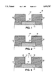
- FIG. 1 is a cross-sectional view of an interconnect structure for a semiconductor device showing an underlying metal layer and a barrier layer, disposed on a dielectric layer and over laid with an inter-level dielectric (ILD) layer, but in which a via opening is formed in the ILD layer to expose a portion of the underlying barrier layer.
- ILD inter-level dielectric
- FIG. 2 is a cross-sectional view showing a formation of a SiN or SiON layer over the ILD layer and also within the via opening of the structure of FIG. 1.
- FIG. 3 is a cross-sectional view showing a formation of a SiN or SiON sidewall within the via opening of FIG. 2 after an anisotropic etch of the SiN or SiON layer.
- FIG. 4 is a cross-sectional view showing the structure of FIG. 3 in which the exposed barrier layer is activated by contact displacement for the electroless deposition of copper.
- FIG. 5 is a cross-sectional view of the structure of FIG. 4 in which copper is electrolessly deposited within the via opening.
- FIG. 6 is a cross-sectional view showing a selective formation of a cap barrier layer atop the copper deposit in the via opening of FIG. 5 in order to form a fully encapsulated copper plug of the present invention.
- FIG. 7 is a cross-sectional view of an interconnect structure similar to the structure shown in FIG. 1, but wherein the barrier layer at the bottom of a via opening is removed, exposing the underlying metal layer.
- FIG. 8 is a cross-sectional view showing a formation of a SiN or SiON layer over the ILD layer and also within the via opening of the structure of FIG. 7.
- FIG. 9 is a cross-sectional view showing a formation of a SiN or SiON sidewall within the via opening of FIG. 8 after an anisotropic etch of the SiN or SiON layer.
- FIG. 10 is a cross-sectional view showing the structure of FIG. 9 in which the exposed metal layer is activated for an electroless deposition of a replacement barrier layer at the bottom of the via opening.
- FIG. 11 is a cross-sectional view of the structure of FIG. 10 in which the bottom barrier layer is selectively formed on the activated surface of the underlying metal layer by electroless deposition and in which the upper surface of the barrier layer is activated by copper contact displacement.
- FIG. 12 is a cross-sectional view of the structure of FIG. 11 in which copper is electrolessly deposited within the via opening atop the newly formed bottom barrier layer.
- FIG. 13 is a cross-sectional view showing a selective formation of a cap barrier layer atop the copper deposit in the via opening of FIG. 12 in order to form an alternative, fully encapsulated copper plug of the present invention.
- FIG. 14 is a cross-sectional view of a semiconductor device having four metal layers and a doped region in a substrate and in which via and contact openings are filled to interconnect the various conductive regions.
- a multiple-metal layer structure atop a wafer substrate, such as a silicon substrate, to manufacture a semiconductor device is well-known in the art.
- dielectric materials such as silicon dioxide (SiO 2 ) are utilized to separate the conductive regions.
- Contact openings are formed in the dielectric overlying the substrate region to provide conductive pathways to the source, drain and gate regions from a first metal layer.
- Via openings are formed in the subsequent inter-level dielectric (ILD) layers separating the various metal layers to provide conductive pathways between the metal layers.
- ILD inter-level dielectric
- One such exemplary multiple metal layer structure is described in "Planar Copper-Polyimide Back End Of The Line Interconnections For ULSI Devices;" B.
- an exemplary semiconductor structure 10 is shown having a metal layer 11 which is covered by an ILD layer 12.
- Metal layer 11 is representative of one of the metal layers in a multiple metal level semiconductor device.
- Layer 12 is typical of an ILD layer separating the different metal layers.
- ILD layer 12 is typically formed from an oxide material, such as silicon dioxide (SiO 2 ). It is appreciated that other materials, such as low dielectric constant materials, polymer and polyimide materials, as well as other non-conductive materials, can be utilized for ILD layer 12.
- metal 11 resides atop a dielectric material (which could be part of layer 12), but what comprises the underlying material is not critical to the understanding of the practice of the present invention. Also, it is understood that structure 10 is only a portion of many structures present on a semiconductor wafer.
- metal wiring layers are fabricated so that a barrier layer is present to separate the copper plug material in via openings from the metal layers forming the wiring.
- Typical practice is to utilize aluminum as the material for the metal lines.
- titanium nitride TiN
- TiN titanium nitride
- metal layer 11 is aluminum, it will have a titanium nitride layer overlying it, so that this titanium nitride layer is noted as layer 13 and will function as a barrier between the aluminum metal and the copper plug.
- the overlying metal can be TiN, titanium tungsten (TiW), tantalum (Ta), TaN or WN.
- TiW titanium tungsten
- Ta tantalum
- TaN tantalum
- WN nickel
- the material used for layer 13 is TiN, since it is presumed that the underlying metal is aluminum.
- a barrier layer 13 is formed overlying the metal layer 11.
- Layer 13 (also referred to as barrier layer 13 herein) is presumed to be TiN and is deposited to a typical thickness of about 200-500 angstroms. The deposition of titanium nitride to form TiN layer 13 is known in the art.
- a via opening (also, via hole or via) 15 is made in ILD 12 in order to provide a pathway to barrier layer 13 and metal 11.
- the via opening 15 will be eventually filled with a conductive material to form an interconnect plug between metal 11 and an overlying metal layer which will be formed above the ILD layer 12.
- the structure 10 of FIG. 1 can be fabricated from a variety of known processes.
- etching process for the formation of the via hole 15 be optimized so that the etch process stops when the TiN layer 13 is reached. The optimization is preferred in order not to etch away the TiN layer 13 at the bottom of the via hole 15.
- a technique of the present invention for forming a copper plug by a technique of selective electroless deposition of copper is described.
- a dielectric encapsulation layer is formed along the sidewalls of via opening 15 in order to inhibit copper migration into the ILD 12.
- a dielectric layer 16 is conformally blanket deposited on the wafer over ILD layer 12 and the exposed portions of TiN layer 13 within via 15.
- silicon nitride (SiN) or silicon oxynitride (SiON) is deposited by a chemical vapor deposition (CVD) technique to a thickness of approximately 500-1500 angstroms.
- the CVD deposited layer 16 has good step coverage and conformity over the via opening 15.
- an anisotropic etch is performed to remove the SiN or SiON layer 16 on the surface of the wafer and at the bottom of the via 15.
- reactive ion etching RIE
- anisotropically etch layer 16 Due to the anisotropic etching, the SiN or SiON layer 16 remains on the vertical sidewalls 17 of via 15.
- the selectivity of the anisotropic dielectric etch over TiN must be carefully maximized in order to retain the TiN layer 13 at the bottom of the via 15. With the presently described technique, approximately 50% (250-750 angstroms) of the SiN or SiON material will remain as sidewall layer 17 on the sidewalls of via 15.
- a technique of the present invention is used to activate the surface of TiN layer 13 by a method of contact displacement of copper.
- activation of a metal is necessary in order to pursue the autocatalytic reaction for the electroless deposition of copper.
- a number of techniques are known for treating a metal surface in order to make the surface susceptible for the autocatalytic reaction.
- the use of palladium (or palladium seeds) is one known technique for treating a surface to start the autocatalytic reaction of copper. (See for example, "Development Of An Electroless Copper Deposition Bath For Via Fill Applications On TiN Seed Layers;" Palmans et al.; Conference Proceedings, ULSI-X; Materials Research Society; 1995; pp. 87-94).
- Pd palladium
- the presence of Pd will reduce the stability of electroless Cu deposition solution and the formation of CuPd alloy increases the resistivity of electroless Cu deposits.
- the present invention uses copper as the activation material for activating the surface by contact displacement.
- the surface of the TiN layer 13 is activated by having a formation of copper atoms 21 attached to its surface by contact displacement, as shown in FIG. 4.
- the preferred material for barrier layer 13 is TiN, but other metallic barrier material can be used as well, provided that the copper activation of the surface can be achieved by contact displacement.
- the complete wafer (incorporating the structure) is subjected to one of two techniques for the formation of the copper layer 21 on the surface of the TiN layer 13.
- the wafer can be dipped in a wet bath containing a contact displacement deposition solution (technique of immersion deposition) or the wafer can be placed on a rotating chuck where the contact displacement solution is injected on to the rotating wafer (technique of spin or shower deposition).
- the aqueous contact displacement solution is formed having de-ionized (DI) water as the main component of the solution.
- DI de-ionized
- the various chemicals noted below are then added to the DI water in quantities noted.
- the solution is further comprised of 0.001-2 mol/liter of Cu +2 ions, 0.001-5 mol/liter of F - ions and 0.01-10 gm/liter of surfactant material.
- the particular solution utilized in the practice of the present invention includes copper sulfate (CuSO 4 ) and hydrofluoric acid (HF) to provide the copper and fluorine ions.
- the particular surfactant used in the solution is comprised of RHODAFAC RE 610 (manufactured by Rhone-Poulenc), polyethylene glycol and Triton X-100 (both manufactured by Aldrich).
- the exposed TiN is subjected to this solution for a time period of approximately 1-600 seconds at a temperature in the approximate range of 18-25° C.
- the parameters can be varied, but ultimately it is desirable to form a copper activation layer 21, having at least a mono-layer of copper atoms to cover the surface of TiN layer 13. Then, the wafer is removed from the contact displacement solution and rinsed in DI water.
- a copper activation layer 21 is formed on the surface of the TiN layer 13, so that now an auto-catalytic deposition of electrolessly deposited copper can occur on the TiN layer 13, once the wafer is placed in an electroless deposition solution.
- the contact displacement technique is described in reference to TiN, since TiN is the preferred barrier material for aluminum metal, but the same copper contact displacement technique can be used with other barrier metals (including those noted earlier) to activate the metal surface for copper deposition.
- Examples of metals, other than TiN, in which copper activation can occur by contact displacement are Al, AlCu, AlSiCu, Ti, Ta, TaN, W, WN and TiW.
- layer 13 can be comprised of one of these other materials, instead of TiN.
- the wafer is rinsed in DI water to remove the activation solution.
- Copper activation of TiN barrier layer by contact displacement is also described in a patent application titled “Electroless Cu Deposition On A Barrier Layer By Cu Contact Displacement For ULSI Applications;" Ser. No. 08/587,262; filed Jan. 16, 1996, which is incorporated by reference herein.
- copper is deposited by the technique of selective electroless deposition of copper to form plug 23.
- the electroless deposition of copper occurs at those locations where copper atoms 21 have activated the TiN surface, which in this instance is at the bottom of via 15 only.
- a selective growth of electrolessly deposited copper forms from TiN layer 13 to selectively fill via opening 15.
- electroless copper deposition solutions can be utilized to electrolessly deposit copper on layer 13.
- the electroless copper deposition to selectively form plug 23 is performed in the following solution.
- the electroless solution of the preferred embodiment is comprised of copper sulfate to supply the Cu 2+ cations, ethylenediaminetetraacetic acid (EDTA) as a complexing agent for Cu 2+ cations, quaternary ammonium hydroxides to supply the OH - , formaldehyde (HCHO) or glyoxylic acid as a reducing agent, RHODAFAC RE 610 or polyethylene glycols as a surfactant and wetting agent, and ammonium cyanide or 2,2"-dipyridyl as stabilizer and ductility promoter.
- EDTA ethylenediaminetetraacetic acid
- HCHO formaldehyde
- RHODAFAC RE 610 polyethylene glycols as a surfactant and wetting agent
- ammonium cyanide or 2,2"-dipyridyl as stabilizer and ductility promoter.
- the particular solution concentration for the solution of the preferred embodiment is mixed in DI water and is comprised of 0.016-0.08 mol/liter of copper sulfate (CuSO 4 ), 0.04-0.2 mol/liter of EDTA, 0.13-1 mol/liter of formaldehyde, 0.06-0.2 mol/liter of glyoxylic acid, 0.01 mol/liter of ammonium cyanide, 10-120 parts-per-million (ppm) of 2,2'-dipyridyl, 50-100 ppm of polyethylene glycol and 0.01-10 gm/liter of RHODAFAC RE 610. Also, sufficient tetramethylammonium hydroxide (TMAH) is added to adjust the pH of the solution to a range of 11-13. The electroless bath is maintained at a temperature in the range of 30°-80° C.
- CuSO 4 copper sulfate
- EDTA 0.13-1 mol/liter of formaldehyde
- Electroless copper deposition reaction can be expressed as:
- the ratio between the components in the solution must be in molar as:
- the wafer is rinsed in DI water again to remove the electroless deposition solution. It is appreciated that the selective growth of copper is timed so that it does not over flow via opening 15. It is also preferable to stop the copper deposition before the via is completely filled. The reason for it is noted below.
- a cap layer 24 is then selectively formed atop the copper plug in via 15.
- the cap layer 24 operates as a barrier layer to fully encapsulate the plug within via 15 and ensures that copper will not migrate out of via 15.
- the cap layer 24 can be formed from a variety of metals or metal alloys which have a barrier property to prevent copper diffusion.
- electrolessly deposited nickel (Ni), cobalt (Co), Ni--Co alloy, CoP, NiCoP or NiP can be used as the material for forming cap layer 24. It is also preferred that the material selected maintains a diffusion barrier at temperatures encountered in subsequent processing steps. Thus, it is preferred that the material selected for cap layer 24 can inhibit copper diffusion at least up to 400° C.
- the cap layer 24 is grown in another bath solution after the electroless copper deposition step. After a rinse, the wafer is placed into a known electroless deposition solution, which solution will depend on the material being deposited (see for example, "Electrochemically Deposited Diffusion Barriers;” Milan Paunovic et al.; J. Electrochem. Soc., Vol. 141, No.7; July 1994; pp. 1843-1850). Typical thickness for the barrier cap layer 24 is in the approximate range of 500-1500 angstroms. Thus, it is to be noted that the cap layer 24 functions as a diffusion barrier layer at the top of plug 23.
- the formation of the SiN or SiON sidewalls 17 in via 15 functions to provide a barrier layer to prevent the diffusion of copper into the ILD 12.
- copper plug 23 is completely isolated from the surrounding ILD 12 by the dielectric sidewall 17.
- the barrier metals 13 and 24 disposed at the bottom and top of the copper plug 23 function to prevent copper diffusion into the adjacent metal layers, thereby allowing for Al wiring to be used with the copper plug.
- the electrolessly deposited copper plug 23 is fully encapsulated along interfaces with adjacent materials.
- dielectric materials can be readily used instead of SiN or SiON for forming sidewall layers 16.
- the requirements for such layer 16 are that it must provide sufficient barrier isolation to inhibit copper diffusion into the adjacent ILD 12 and it must be compatible with the subsequent contact displacement process for forming the copper activation layer 21.
- the deposition can be stopped prior to the top of the plug reaching the upper surface of ILD layer 12.
- the electroless copper deposition is stopped below the surface with ample room for the formation of cap layer 24.
- Forming the cap layer 24 within via opening 15 so that the upper surface of cap layer 24 is substantially planar with the surface of ILD layer 12 completes the plug formation.
- CMP steps to polish and planarize the upper surface of the plug is not needed. It is appreciated that some amount of overgrowth can be tolerated, however, any significant overgrowth will require CMP to planarize the surface for proper Cu encapsulation.
- the fully encapsulated copper plug is then annealed at a temperature in the range of 150°-200° C. in vacuum for a time period of 0.5-1 hour.
- CMP can be used to planarize the surface of the copper plug.
- the preference is not to require the CMP step.
- the cap layer 24 may not be needed.
- this barrier layer can be used in place of the cap barrier layer 24.
- it is preferable to grow the copper plug so that the upper surface of the plug is substantially planar to the surface of the ILD where the barrier layer is to be deposited. To some extent, slight undergrowth of the plug is permitted.
- FIGS. 7-13 An alternative embodiment is shown in reference to FIGS. 7-13.
- the structure of FIG. 7 is equivalent to the structure of FIG. 1 except that the exposed TiN layer 13 in the via opening 15 has been etched away during the etch process creating the via opening 15. This is not preferred, but may occur with certain etch chemistries and/or processes. Accordingly, the underlying metal 11 is exposed in via 15. Thus, in order to practice the present invention, an additional step of reforming a barrier layer at the bottom of via opening 15 is necessary in order to encapsulate the copper plug.
- the SiN or SiON layer 16 is first conformally deposited as described in reference to FIG. 2.
- the subsequent anisotropic etch (equivalent to FIG. 3) of the SiN or SiON layer 16 is shown in FIG. 9 to form SiN or SiON sidewalls 17.
- the metal layer 11 is still exposed at the bottom of via opening 15.
- a metal barrier layer 19 is deposited in the bottom of the via opening 15 to prevent the diffusion of copper into the metal 11.
- the formation of the bottom barrier layer 19 is shown in FIG. 11.
- the preferred technique is to utilize electroless deposition to selectively form the barrier layer 19. If the underlying metal is aluminum, two techniques can be used to activate the aluminum to form an activation (seed) layer 27 on the aluminum, as shown in FIG. 10.
- a solution equivalent to the solution that was used for the copper contact displacement on TiN is used to activate the aluminum surface to form the activation layer 27.
- palladium (Pd) is used to activate the aluminum surface by a known technique to form the activation layer 27 (see for example, U.S. Pat. No. 4,574,095 and "Selective Electroless Metal Deposition For Via Hole Filling In VLSI Multilevel Interconnection Structures;" C. H. Ting et al.; J. Electrochem. Soc. Vol. 136; 1989; pp. 562).
- the wafer is then rinsed in DI water.
- the wafer is then subjected to an electroless deposition process equivalent to that described for the formation of cap layer 24 to selectively grow the metal barrier layer 19 comprised of one of the materials mentioned for the formation of cap barrier layer 24.
- the barrier layer 19 is electrolessly deposited on the activated surface 27 of metal layer 11.
- the preference is to use electrolessly deposited nickel (Ni), cobalt (Co), Ni--Co alloy, CoP, NiCoP or NiP to selectively form barrier layer 19.
- barrier layer 19 is not catalytic to electroless copper growth, then the surface of the barrier layer 19 is first activated.
- the preferred approach is to use the afore-mentioned copper contact displacement solution to form an activation layer 28 by contact displacement of copper atop barrier layer 19, as shown in FIG. 11. Once the barrier layer 19 is activated, the electroless copper deposition can occur to form plug 23, as shown in FIG. 12.
- the surface of the barrier layer 19 need not be treated (activated) in a separate step to form the activation layer 28.
- the reducing agent is dimethyllamine borane (DMAB).
- DMAB dimethyllamine borane
- One typical electroless Cu deposition solution using DMAB as a reducing agent can be found in "Electroless plating of copper at a low pH level;” R. Jagannathan et al.; IBM J. Res. Develop. Vol. 37, No. 2; March 1993; pp. 117-123.
- the wafer can be subjected to the electroless copper deposition solution without first having the surface of the barrier layer 19 activated.
- FIG. 14 shows a three-metal level structure 50 in which the metal levels are designated M1, M2 and M3, separated by dielectric layers 55. Plugs 51 are used to couple the metal lines 52 to each other and the Mr level to a contact region 53 on a substrate 54. It is appreciated that the present invention can be readily used to provide for the various plugs 51 shown in FIG. 14 in the fabrication of semiconductor devices.
- an electroless copper deposition technique in which advantages associated with the use of copper for conductive paths in a semiconductor device are inherently present in the practice of the present invention.
- the present invention is not limited to the size of the device or the via opening, but has advantages at smaller sized dimensions in the submicron range (typically in the approximate range of 0.2-0.8 ⁇ m).
- the practice of the present invention allows higher aspect ratio structures, including vias, to be fabricated.
- CMP is not needed to planarize the plug surface after the selective formation of the plug in the via opening.
- the electroless copper deposition can be performed as a batch process in which a substantial number of wafers can be immersed in the wet bath at the same time.
Abstract
Description
2HCHO+{Cu EDTA!}.sup.2- +4OH.sup.- →Cu+H.sub.2 +2HCOO.sup.- +2H.sub.2 O+EDTA.sup.4-
1 mol Cu.sup.2+ : 2 mol HCHO: 1 mol EDTA.sup.4-
Claims (32)
Priority Applications (1)
| Application Number | Priority Date | Filing Date | Title |
|---|---|---|---|
| US08/587,263 US5674787A (en) | 1996-01-16 | 1996-01-16 | Selective electroless copper deposited interconnect plugs for ULSI applications |
Applications Claiming Priority (1)
| Application Number | Priority Date | Filing Date | Title |
|---|---|---|---|
| US08/587,263 US5674787A (en) | 1996-01-16 | 1996-01-16 | Selective electroless copper deposited interconnect plugs for ULSI applications |
Publications (1)
| Publication Number | Publication Date |
|---|---|
| US5674787A true US5674787A (en) | 1997-10-07 |
Family
ID=24349076
Family Applications (1)
| Application Number | Title | Priority Date | Filing Date |
|---|---|---|---|
| US08/587,263 Expired - Fee Related US5674787A (en) | 1996-01-16 | 1996-01-16 | Selective electroless copper deposited interconnect plugs for ULSI applications |
Country Status (1)
| Country | Link |
|---|---|
| US (1) | US5674787A (en) |
Cited By (475)
| Publication number | Priority date | Publication date | Assignee | Title |
|---|---|---|---|---|
| US5872063A (en) * | 1998-01-12 | 1999-02-16 | Taiwan Semiconductor Manufacturing Company Ltd. | Self-aligned contact structures using high selectivity etching |
| US5891513A (en) * | 1996-01-16 | 1999-04-06 | Cornell Research Foundation | Electroless CU deposition on a barrier layer by CU contact displacement for ULSI applications |
| US5913147A (en) * | 1997-01-21 | 1999-06-15 | Advanced Micro Devices, Inc. | Method for fabricating copper-aluminum metallization |
| US5918150A (en) * | 1996-10-11 | 1999-06-29 | Sharp Microelectronics Technology, Inc. | Method for a chemical vapor deposition of copper on an ion prepared conductive surface |
| US5953628A (en) * | 1997-01-28 | 1999-09-14 | Matsushita Electric Industrial Co., Ltd. | Method for forming wiring for a semiconductor device |
| US5985762A (en) * | 1997-05-19 | 1999-11-16 | International Business Machines Corporation | Method of forming a self-aligned copper diffusion barrier in vias |
| US6001415A (en) * | 1997-12-03 | 1999-12-14 | Advanced Micro Devices, Inc. | Via with barrier layer for impeding diffusion of conductive material from via into insulator |
| US6008117A (en) * | 1996-03-29 | 1999-12-28 | Texas Instruments Incorporated | Method of forming diffusion barriers encapsulating copper |
| US6010962A (en) * | 1999-02-12 | 2000-01-04 | Taiwan Semiconductor Manufacturing Company | Copper chemical-mechanical-polishing (CMP) dishing |
| US6015749A (en) * | 1998-05-04 | 2000-01-18 | Taiwan Semiconductor Manufacturing Company | Method to improve adhesion between copper and titanium nitride, for copper interconnect structures, via the use of an ion implantation procedure |
| WO2000003420A2 (en) * | 1998-07-10 | 2000-01-20 | Cvc, Inc. | Method for forming a copper film on a substrate |
| WO2000004573A1 (en) * | 1998-07-16 | 2000-01-27 | National University Of Singapore | Highly selective and complete interconnect metal line and via/contact hole filling by electroless plating |
| US6022808A (en) * | 1998-03-16 | 2000-02-08 | Advanced Micro Devices, Inc. | Copper interconnect methodology for enhanced electromigration resistance |
| US6025275A (en) * | 1996-12-19 | 2000-02-15 | Texas Instruments Incorporated | Method of forming improved thick plated copper interconnect and associated auxiliary metal interconnect |
| FR2782839A1 (en) * | 1998-03-30 | 2000-03-03 | Sony Corp | Fabrication of a semiconductor device, especially an integrated circuit device, comprises forming a conductor in a concave opening by depositing an electroless first conductor film |
| US6037258A (en) * | 1999-05-07 | 2000-03-14 | Taiwan Semiconductor Manufacturing Company | Method of forming a smooth copper seed layer for a copper damascene structure |
| US6046107A (en) * | 1998-12-17 | 2000-04-04 | Industrial Technology Research Institute | Electroless copper employing hypophosphite as a reducing agent |
| EP0991114A2 (en) * | 1998-10-01 | 2000-04-05 | Chartered Semiconductor Manufacturing Pte Ltd. | Ultra-low sheet resistance metal/poly-SI gate for deep sub-micron CMOS application |
| WO2000019522A1 (en) * | 1998-09-29 | 2000-04-06 | Conexant Systems, Inc. | Improved methods for barrier layer formation |
| US6051490A (en) * | 1991-11-29 | 2000-04-18 | Sony Corporation | Method of forming wirings |
| US6066557A (en) * | 1998-12-09 | 2000-05-23 | Advanced Micro Devices, Inc. | Method for fabricating protected copper metallization |
| US6077771A (en) * | 1998-04-20 | 2000-06-20 | United Silicon Incorporated | Method for forming a barrier layer |
| US6086777A (en) * | 1998-07-02 | 2000-07-11 | Advanced Micro Devices, Inc. | Tantalum barrier metal removal by using CF4 /o2 plasma dry etch |
| EP1019954A1 (en) * | 1998-02-04 | 2000-07-19 | Semitool, Inc. | Method and apparatus for low-temperature annealing of metallization micro-structures in the production of a microelectronic device |
| EP1022770A2 (en) * | 1999-01-22 | 2000-07-26 | Sony Corporation | Method and apparatus for plating and plating structure |
| US6100182A (en) * | 1997-06-23 | 2000-08-08 | Hyundai Electronics Industries, Co., Ltd. | Method for forming metal interconnection of semiconductor device |
| US6100196A (en) * | 1996-04-08 | 2000-08-08 | Chartered Semiconductor Manufacturing Ltd. | Method of making a copper interconnect with top barrier layer |
| US6100195A (en) * | 1998-12-28 | 2000-08-08 | Chartered Semiconductor Manu. Ltd. | Passivation of copper interconnect surfaces with a passivating metal layer |
| US6107208A (en) * | 1998-06-04 | 2000-08-22 | Advanced Micro Devices, Inc. | Nitride etch using N2 /Ar/CHF3 chemistry |
| US6110817A (en) * | 1999-08-19 | 2000-08-29 | Taiwan Semiconductor Manufacturing Company | Method for improvement of electromigration of copper by carbon doping |
| US6114238A (en) * | 1998-01-26 | 2000-09-05 | United Silicon Incorporated | Self-aligned metal nitride for copper passivation |
| US6130162A (en) * | 1999-01-04 | 2000-10-10 | Taiwan Semiconductor Manufacturing Company | Method of preparing passivated copper line and device manufactured thereby |
| WO2000063966A2 (en) * | 1999-04-01 | 2000-10-26 | Cvc Products, Inc. | Method for planarized deposition of a material |
| US6143657A (en) * | 1999-01-04 | 2000-11-07 | Taiwan Semiconductor Manufacturing Company | Method of increasing the stability of a copper to copper interconnection process and structure manufactured thereby |
| US6150206A (en) * | 1997-04-29 | 2000-11-21 | Samsung Electronics Co., Ltd. | Methods of forming integrated circuit capacitors using trench isolation and planarization techniques |
| US6150269A (en) * | 1998-09-11 | 2000-11-21 | Chartered Semiconductor Manufacturing Company, Ltd. | Copper interconnect patterning |
| WO2000075964A2 (en) * | 1999-06-05 | 2000-12-14 | Kim Ki Bum | Method of fabricating semiconductor device employing copper interconnect structure |
| US6169024B1 (en) | 1998-09-30 | 2001-01-02 | Intel Corporation | Process to manufacture continuous metal interconnects |
| US6180523B1 (en) | 1998-10-13 | 2001-01-30 | Industrial Technology Research Institute | Copper metallization of USLI by electroless process |
| US6184138B1 (en) | 1999-09-07 | 2001-02-06 | Chartered Semiconductor Manufacturing Ltd. | Method to create a controllable and reproducible dual copper damascene structure |
| US6184128B1 (en) | 2000-01-31 | 2001-02-06 | Advanced Micro Devices, Inc. | Method using a thin resist mask for dual damascene stop layer etch |
| EP1077485A2 (en) * | 1999-08-16 | 2001-02-21 | Chartered Semiconductor Manufacturing Pte Ltd. | Method to deposit a platinum seed layer for use in selective copper plating |
| US6197688B1 (en) | 1998-02-12 | 2001-03-06 | Motorola Inc. | Interconnect structure in a semiconductor device and method of formation |
| US6204204B1 (en) | 1999-04-01 | 2001-03-20 | Cvc Products, Inc. | Method and apparatus for depositing tantalum-based thin films with organmetallic precursor |
| US6208016B1 (en) | 1998-09-10 | 2001-03-27 | Micron Technology, Inc. | Forming submicron integrated-circuit wiring from gold, silver, copper and other metals |
| US6211073B1 (en) | 1998-02-27 | 2001-04-03 | Micron Technology, Inc. | Methods for making copper and other metal interconnections in integrated circuits |
| US6214728B1 (en) * | 1998-11-20 | 2001-04-10 | Chartered Semiconductor Manufacturing, Ltd. | Method to encapsulate copper plug for interconnect metallization |
| US6218302B1 (en) | 1998-07-21 | 2001-04-17 | Motorola Inc. | Method for forming a semiconductor device |
| US6221763B1 (en) | 1999-04-05 | 2001-04-24 | Micron Technology, Inc. | Method of forming a metal seed layer for subsequent plating |
| US6221758B1 (en) | 1999-01-04 | 2001-04-24 | Taiwan Semiconductor Manufacturing Company | Effective diffusion barrier process and device manufactured thereby |
| WO2001029892A1 (en) * | 1999-10-18 | 2001-04-26 | Infineon Technologies North America Corp. | Self-aligned metal caps for interlevel metal connections |
| US6225226B1 (en) | 1999-12-13 | 2001-05-01 | Taiwan Semiconductor Manufacturing Company | Method for processing and integrating copper interconnects |
| US6225223B1 (en) | 1999-08-16 | 2001-05-01 | Taiwan Semiconductor Manufacturing Company | Method to eliminate dishing of copper interconnects |
| US6228768B1 (en) * | 1998-11-02 | 2001-05-08 | Advanced Micro Devices, Inc. | Storage-annealing plated CU interconnects |
| US6251786B1 (en) | 1999-09-07 | 2001-06-26 | Chartered Semiconductor Manufacturing Ltd. | Method to create a copper dual damascene structure with less dishing and erosion |
| US6261954B1 (en) | 2000-02-10 | 2001-07-17 | Chartered Semiconductor Manufacturing, Ltd. | Method to deposit a copper layer |
| US6271135B1 (en) * | 1998-07-07 | 2001-08-07 | Imec Vzx | Method for forming copper-containing metal studs |
| US6274495B1 (en) | 1998-09-03 | 2001-08-14 | Cvc Products, Inc. | Method for fabricating a device on a substrate |
| US6284656B1 (en) | 1998-08-04 | 2001-09-04 | Micron Technology, Inc. | Copper metallurgy in integrated circuits |
| US6287968B1 (en) * | 1999-01-04 | 2001-09-11 | Advanced Micro Devices, Inc. | Method of defining copper seed layer for selective electroless plating processing |
| US6294836B1 (en) | 1998-12-22 | 2001-09-25 | Cvc Products Inc. | Semiconductor chip interconnect barrier material and fabrication method |
| US6300244B1 (en) | 1998-05-25 | 2001-10-09 | Hitachi, Ltd. | Semiconductor device and method of manufacturing the same |
| US6300236B1 (en) * | 1997-09-30 | 2001-10-09 | International Business Machines Corporation | Copper stud structure with refractory metal liner |
| US6303881B1 (en) | 1998-03-20 | 2001-10-16 | Viasystems, Inc. | Via connector and method of making same |
| US6313028B2 (en) * | 1999-03-05 | 2001-11-06 | United Microelectronics Corp. | Method of fabricating dual damascene structure |
| US6316830B1 (en) | 1998-12-17 | 2001-11-13 | Charles Wen Chyang Lin | Bumpless flip chip assembly with strips and via-fill |
| US6344413B1 (en) | 1997-12-22 | 2002-02-05 | Motorola Inc. | Method for forming a semiconductor device |
| US20020022363A1 (en) * | 1998-02-04 | 2002-02-21 | Thomas L. Ritzdorf | Method for filling recessed micro-structures with metallization in the production of a microelectronic device |
| US6350687B1 (en) * | 1999-03-18 | 2002-02-26 | Advanced Micro Devices, Inc. | Method of fabricating improved copper metallization including forming and removing passivation layer before forming capping film |
| US6350386B1 (en) | 2000-09-20 | 2002-02-26 | Charles W. C. Lin | Method of making a support circuit with a tapered through-hole for a semiconductor chip assembly |
| US6350632B1 (en) | 2000-09-20 | 2002-02-26 | Charles W. C. Lin | Semiconductor chip assembly with ball bond connection joint |
| US6350633B1 (en) | 2000-08-22 | 2002-02-26 | Charles W. C. Lin | Semiconductor chip assembly with simultaneously electroplated contact terminal and connection joint |
| US6359328B1 (en) | 1998-12-31 | 2002-03-19 | Intel Corporation | Methods for making interconnects and diffusion barriers in integrated circuits |
| JP2002118111A (en) * | 2000-10-12 | 2002-04-19 | Sony Corp | Semiconductor device and its manufacturing method |
| US6383920B1 (en) | 2001-01-10 | 2002-05-07 | International Business Machines Corporation | Process of enclosing via for improved reliability in dual damascene interconnects |
| US20020053741A1 (en) * | 1998-02-23 | 2002-05-09 | Tomio Iwasaki | Semiconductor device and method for producing the same |
| US20020060363A1 (en) * | 1997-05-14 | 2002-05-23 | Applied Materials, Inc. | Reliability barrier integration for Cu application |
| US6400031B1 (en) * | 1998-06-11 | 2002-06-04 | Oki Electric Industry Co., Ltd. | Semiconductor device having damascene interconnection structure that prevents void formation between interconnections |
| WO2002045155A2 (en) * | 2000-11-29 | 2002-06-06 | Intel Corporation | ELECTROLESS METHOD OF SEED LAYER DEPOSITION, REPAIR, AND FABRICATION OF Cu INTERCONNECTS |
| US6402970B1 (en) | 2000-08-22 | 2002-06-11 | Charles W. C. Lin | Method of making a support circuit for a semiconductor chip assembly |
| US6403460B1 (en) | 2000-08-22 | 2002-06-11 | Charles W. C. Lin | Method of making a semiconductor chip assembly |
| US6403400B2 (en) | 1998-12-17 | 2002-06-11 | Charles Wen Chyang Lin | Bumpless flip chip assembly with strips-in-via and plating |
| US6406939B1 (en) | 1998-05-02 | 2002-06-18 | Charles W. C. Lin | Flip chip assembly with via interconnection |
| US6410435B1 (en) | 1999-10-01 | 2002-06-25 | Agere Systems Guardian Corp. | Process for fabricating copper interconnect for ULSI integrated circuits |
| US6436734B1 (en) | 2000-08-22 | 2002-08-20 | Charles W. C. Lin | Method of making a support circuit for a semiconductor chip assembly |
| US6440835B1 (en) | 2000-10-13 | 2002-08-27 | Charles W. C. Lin | Method of connecting a conductive trace to a semiconductor chip |
| US6441492B1 (en) | 1999-09-10 | 2002-08-27 | James A. Cunningham | Diffusion barriers for copper interconnect systems |
| US6444489B1 (en) | 2000-12-15 | 2002-09-03 | Charles W. C. Lin | Semiconductor chip assembly with bumped molded substrate |
| US6444263B1 (en) | 2000-09-15 | 2002-09-03 | Cvc Products, Inc. | Method of chemical-vapor deposition of a material |
| US6448644B1 (en) | 1998-05-02 | 2002-09-10 | Charles W. C. Lin | Flip chip assembly with via interconnection |
| US6448108B1 (en) | 2000-10-02 | 2002-09-10 | Charles W. C. Lin | Method of making a semiconductor chip assembly with a conductive trace subtractively formed before and after chip attachment |
| US20020127845A1 (en) * | 1999-03-01 | 2002-09-12 | Paul A. Farrar | Conductive structures in integrated circuits |
| US6455937B1 (en) * | 1998-03-20 | 2002-09-24 | James A. Cunningham | Arrangement and method for improved downward scaling of higher conductivity metal-based interconnects |
| US6455424B1 (en) * | 2000-08-07 | 2002-09-24 | Micron Technology, Inc. | Selective cap layers over recessed polysilicon plugs |
| US6454916B1 (en) | 2000-01-05 | 2002-09-24 | Advanced Micro Devices, Inc. | Selective electroplating with direct contact chemical polishing |
| US6479384B2 (en) * | 2000-02-18 | 2002-11-12 | Sony Corporation | Process for fabricating a semiconductor device |
| US20020173142A1 (en) * | 2001-02-15 | 2002-11-21 | Serge Vanhaelemeersch | Method of fabricating a semiconductor device |
| US6492252B1 (en) | 2000-10-13 | 2002-12-10 | Bridge Semiconductor Corporation | Method of connecting a bumped conductive trace to a semiconductor chip |
| US20020187631A1 (en) * | 2000-12-06 | 2002-12-12 | Ki-Bum Kim | Copper interconnect structure having stuffed diffusion barrier |
| US6495200B1 (en) | 1998-12-07 | 2002-12-17 | Chartered Semiconductor Manufacturing Ltd. | Method to deposit a seeding layer for electroless copper plating |
| US6511865B1 (en) | 2000-09-20 | 2003-01-28 | Charles W. C. Lin | Method for forming a ball bond connection joint on a conductive trace and conductive pad in a semiconductor chip assembly |
| US6521532B1 (en) * | 1999-07-22 | 2003-02-18 | James A. Cunningham | Method for making integrated circuit including interconnects with enhanced electromigration resistance |
| US6528891B2 (en) | 1998-12-17 | 2003-03-04 | Charles Wen Chyang Lin | Bumpless flip chip assembly with solder via |
| US6537851B1 (en) | 2000-10-13 | 2003-03-25 | Bridge Semiconductor Corporation | Method of connecting a bumped compliant conductive trace to a semiconductor chip |
| US6544891B1 (en) * | 2001-09-04 | 2003-04-08 | Taiwan Semiconductor Manufacturing Company | Method to eliminate post-CMP copper flake defect |
| US6544813B1 (en) | 2000-10-02 | 2003-04-08 | Charles W. C. Lin | Method of making a semiconductor chip assembly with a conductive trace subtractively formed before and after chip attachment |
| US6548393B1 (en) | 2000-10-13 | 2003-04-15 | Charles W. C. Lin | Semiconductor chip assembly with hardened connection joint |
| US20030073314A1 (en) * | 2001-10-11 | 2003-04-17 | Epion Corporation | GCIB processing to improve interconnection vias and improved interconnection via |
| US6551861B1 (en) | 2000-08-22 | 2003-04-22 | Charles W. C. Lin | Method of making a semiconductor chip assembly by joining the chip to a support circuit with an adhesive |
| US6551872B1 (en) | 1999-07-22 | 2003-04-22 | James A. Cunningham | Method for making integrated circuit including interconnects with enhanced electromigration resistance using doped seed layer and integrated circuits produced thereby |
| US6555171B1 (en) | 2000-04-26 | 2003-04-29 | Advanced Micro Devices, Inc. | Cu/Sn/Pd activation of a barrier layer for electroless CU deposition |
| US6559061B2 (en) | 1998-07-31 | 2003-05-06 | Applied Materials, Inc. | Method and apparatus for forming improved metal interconnects |
| US6562709B1 (en) | 2000-08-22 | 2003-05-13 | Charles W. C. Lin | Semiconductor chip assembly with simultaneously electroplated contact terminal and connection joint |
| US6562715B1 (en) | 2000-08-09 | 2003-05-13 | Applied Materials, Inc. | Barrier layer structure for copper metallization and method of forming the structure |
| US6562657B1 (en) | 2000-08-22 | 2003-05-13 | Charles W. C. Lin | Semiconductor chip assembly with simultaneously electrolessly plated contact terminal and connection joint |
| US6565729B2 (en) | 1998-03-20 | 2003-05-20 | Semitool, Inc. | Method for electrochemically depositing metal on a semiconductor workpiece |
| US6573606B2 (en) * | 2001-06-14 | 2003-06-03 | International Business Machines Corporation | Chip to wiring interface with single metal alloy layer applied to surface of copper interconnect |
| US6576539B1 (en) | 2000-10-13 | 2003-06-10 | Charles W.C. Lin | Semiconductor chip assembly with interlocked conductive trace |
| US6576493B1 (en) | 2000-10-13 | 2003-06-10 | Bridge Semiconductor Corporation | Method of connecting a conductive trace and an insulative base to a semiconductor chip using multiple etch steps |
| US20030109129A1 (en) * | 2001-11-15 | 2003-06-12 | Tatsuyuki Saito | Semiconductor device |
| US6583040B1 (en) | 2000-10-13 | 2003-06-24 | Bridge Semiconductor Corporation | Method of making a pillar in a laminated structure for a semiconductor chip assembly |
| US20030119324A1 (en) * | 2001-12-26 | 2003-06-26 | Jung Jong Goo | Method for manufacturing metal line contact plug of semiconductor device |
| JP2003179000A (en) * | 2001-12-12 | 2003-06-27 | Sony Corp | Semiconductor device and method of manufacturing the same |
| US20030134503A1 (en) * | 1997-10-09 | 2003-07-17 | Werner Juengling | Methods of forming materials between conductive electrical components, and insulating materials |
| US6598291B2 (en) | 1998-03-20 | 2003-07-29 | Viasystems, Inc. | Via connector and method of making same |
| US20030141194A1 (en) * | 1998-03-20 | 2003-07-31 | Chen Linlin | Apparatus and method for electrolytically depositing copper on a semiconductor workpiece |
| US20030140988A1 (en) * | 2002-01-28 | 2003-07-31 | Applied Materials, Inc. | Electroless deposition method over sub-micron apertures |
| US6627995B2 (en) | 2000-03-03 | 2003-09-30 | Cvc Products, Inc. | Microelectronic interconnect material with adhesion promotion layer and fabrication method |
| US20030190812A1 (en) * | 2002-04-03 | 2003-10-09 | Deenesh Padhi | Electroless deposition method |
| US20030189026A1 (en) * | 2002-04-03 | 2003-10-09 | Deenesh Padhi | Electroless deposition method |
| US6640151B1 (en) | 1999-12-22 | 2003-10-28 | Applied Materials, Inc. | Multi-tool control system, method and medium |
| US20030202070A1 (en) * | 2002-04-29 | 2003-10-30 | Xerox Corporation | Multiple portion solid ink stick |
| US20030207561A1 (en) * | 2002-05-03 | 2003-11-06 | Dubin Valery M. | Interconnect structures containing conductive electrolessly deposited etch stop layers, liner layers, and via plugs |
| US6649511B1 (en) * | 2000-11-06 | 2003-11-18 | Advanced Micro Devices, Inc. | Method of manufacturing a seed layer with annealed region for integrated circuit interconnects |
| US20030216025A1 (en) * | 2002-05-16 | 2003-11-20 | Haijing Lu | Wafer level electroless copper metallization and bumping process, and plating solutions for semiconductor wafer and microchip |
| US6653170B1 (en) | 2001-02-06 | 2003-11-25 | Charles W. C. Lin | Semiconductor chip assembly with elongated wire ball bonded to chip and electrolessly plated to support circuit |
| US6660626B1 (en) | 2000-08-22 | 2003-12-09 | Charles W. C. Lin | Semiconductor chip assembly with simultaneously electrolessly plated contact terminal and connection joint |
| US20030228749A1 (en) * | 2002-06-06 | 2003-12-11 | Nishant Sinha | Plating metal caps on conductive interconnect for wirebonding |
| US6664122B1 (en) | 2001-10-19 | 2003-12-16 | Novellus Systems, Inc. | Electroless copper deposition method for preparing copper seed layers |
| US6667229B1 (en) | 2000-10-13 | 2003-12-23 | Bridge Semiconductor Corporation | Method of connecting a bumped compliant conductive trace and an insulative base to a semiconductor chip |
| US20030235983A1 (en) * | 2002-06-21 | 2003-12-25 | Nanhai Li | Temperature control sequence of electroless plating baths |
| US6686280B1 (en) | 1999-07-22 | 2004-02-03 | Taiwan Semiconductor Manufacturing Company | Sidewall coverage for copper damascene filling |
| US20040023480A1 (en) * | 2001-08-16 | 2004-02-05 | Dennison Charles H. | Semiconductor processing methods, and semiconductor assemblies |
| US20040038052A1 (en) * | 2002-08-21 | 2004-02-26 | Collins Dale W. | Microelectronic workpiece for electrochemical deposition processing and methods of manufacturing and using such microelectronic workpieces |
| US6699780B1 (en) | 2000-10-13 | 2004-03-02 | Bridge Semiconductor Corporation | Method of connecting a conductive trace to a semiconductor chip using plasma undercut etching |
| US20040041273A1 (en) * | 2002-08-30 | 2004-03-04 | Chia-Hong Jan | Structure and manufacturing process of localized shunt to reduce electromigration failure of copper dual damascene process |
| US6708074B1 (en) | 2000-08-11 | 2004-03-16 | Applied Materials, Inc. | Generic interface builder |
| US6709874B2 (en) * | 2001-01-24 | 2004-03-23 | Infineon Technologies Ag | Method of manufacturing a metal cap layer for preventing damascene conductive lines from oxidation |
| US20040087148A1 (en) * | 2002-10-30 | 2004-05-06 | Xerox Corporation | Copper interconnect by immersion/electroless plating in dual damascene process |
| US20040087141A1 (en) * | 2002-10-30 | 2004-05-06 | Applied Materials, Inc. | Post rinse to improve selective deposition of electroless cobalt on copper for ULSI application |
| US6740576B1 (en) | 2000-10-13 | 2004-05-25 | Bridge Semiconductor Corporation | Method of making a contact terminal with a plated metal peripheral sidewall portion for a semiconductor chip assembly |
| US6740580B1 (en) | 1999-09-03 | 2004-05-25 | Chartered Semiconductor Manufacturing Ltd. | Method to form copper interconnects by adding an aluminum layer to the copper diffusion barrier |
| US6743716B2 (en) | 2000-01-18 | 2004-06-01 | Micron Technology, Inc. | Structures and methods to enhance copper metallization |
| US20040113277A1 (en) * | 2002-12-11 | 2004-06-17 | Chiras Stefanie Ruth | Formation of aligned capped metal lines and interconnections in multilevel semiconductor structures |
| US6756298B2 (en) | 2000-01-18 | 2004-06-29 | Micron Technology, Inc. | Methods and apparatus for making integrated-circuit wiring from copper, silver, gold, and other metals |
| US20040137733A1 (en) * | 2002-11-08 | 2004-07-15 | Epion Corporation | GCIB processing of integrated circuit interconnect structures |
| US20040142114A1 (en) * | 2003-01-21 | 2004-07-22 | Mattson Technology, Inc. | Electroless plating solution and process |
| US6778302B2 (en) | 2000-03-02 | 2004-08-17 | Sony Corporation | Holographic stereogram printing system, holographic stereogram printing method and holographing device |
| US6787467B2 (en) * | 1997-09-18 | 2004-09-07 | Ebara Corporation | Method of forming embedded copper interconnections and embedded copper interconnection structure |
| US6806578B2 (en) * | 2000-03-16 | 2004-10-19 | International Business Machines Corporation | Copper pad structure |
| US6811675B2 (en) | 1998-03-20 | 2004-11-02 | Semitool, Inc. | Apparatus and method for electrolytically depositing copper on a semiconductor workpiece |
| US20040219298A1 (en) * | 2003-02-27 | 2004-11-04 | Akira Fukunaga | Substrate processing method and substrate processing apparatus |
| US20040224497A1 (en) * | 2003-05-05 | 2004-11-11 | Hans-Joachim Barth | Method to form selective cap layers on metal features with narrow spaces |
| US20040235237A1 (en) * | 2001-06-11 | 2004-11-25 | Hiroaki Inoue | Semiconductor device and method for manufacturing the same |
| US20040238963A1 (en) * | 2003-05-26 | 2004-12-02 | Renesas Technology Corp. | Semiconductor device having structure for connecting interconnect lines |
| US20040253814A1 (en) * | 2003-06-10 | 2004-12-16 | Chin-Chang Cheng | Method for improving selectivity of electroless metal deposition |
| US20040258848A1 (en) * | 2003-05-23 | 2004-12-23 | Akira Fukunaga | Method and apparatus for processing a substrate |
| US20050009213A1 (en) * | 2003-06-27 | 2005-01-13 | Xinming Wang | Substrate processing method and apparatus |
| US20050029669A1 (en) * | 2003-07-17 | 2005-02-10 | Hiroaki Inoue | Semiconductor device and method for manufacturing the same |
| US20050034303A1 (en) * | 2001-08-03 | 2005-02-17 | Schlumberger Systemes | Process to allow electrical and mechanical connection of an electrical device with a face equipped with contact pads |
| KR100474857B1 (en) * | 2002-06-29 | 2005-03-10 | 매그나칩 반도체 유한회사 | Method for forming a copper metal line in semiconductor device |
| US20050059231A1 (en) * | 2000-10-26 | 2005-03-17 | Matsushita Electric Industrial Co., Ltd. | Semiconductor device and method for fabricating the same |
| US20050064707A1 (en) * | 2003-09-23 | 2005-03-24 | Nishant Sinha | Process and integration scheme for fabricating conductive components, through-vias and semiconductor components including conductive through-wafer vias |
| US20050064702A1 (en) * | 2003-07-24 | 2005-03-24 | Xinming Wang | Interconnects forming method and interconnects forming apparatus |
| US6872591B1 (en) | 2000-10-13 | 2005-03-29 | Bridge Semiconductor Corporation | Method of making a semiconductor chip assembly with a conductive trace and a substrate |
| US20050069646A1 (en) * | 2003-06-13 | 2005-03-31 | Hiroaki Inoue | Plating method, plating apparatus and interconnects forming method |
| US6876072B1 (en) | 2000-10-13 | 2005-04-05 | Bridge Semiconductor Corporation | Semiconductor chip assembly with chip in substrate cavity |
| US20050077630A1 (en) * | 2003-10-09 | 2005-04-14 | Kirby Kyle K. | Methods of plating via interconnects |
| US20050085066A1 (en) * | 2003-10-16 | 2005-04-21 | Taiwan Semicondutor Manufacturing Co. | Novel method to reduce Rs pattern dependence effect |
| US20050083592A1 (en) * | 2003-09-10 | 2005-04-21 | Yaakov Amitai | High Brightness optical device |
| US20050081785A1 (en) * | 2003-10-15 | 2005-04-21 | Applied Materials, Inc. | Apparatus for electroless deposition |
| US20050092611A1 (en) * | 2003-11-03 | 2005-05-05 | Semitool, Inc. | Bath and method for high rate copper deposition |
| KR100469338B1 (en) * | 1997-12-30 | 2005-05-17 | 주식회사 하이닉스반도체 | MOS PET Metal Film Formation Method |
| US20050112856A1 (en) * | 2002-09-23 | 2005-05-26 | Dubin Valery M. | Seed layer treatment |
| KR100493428B1 (en) * | 2000-12-30 | 2005-06-07 | 주식회사 하이닉스반도체 | Method for Polishing Electrode lines of a Semiconductor Device |
| US20050124158A1 (en) * | 2003-10-15 | 2005-06-09 | Lopatin Sergey D. | Silver under-layers for electroless cobalt alloys |
| US20050121794A1 (en) * | 1997-10-09 | 2005-06-09 | Werner Juengling | Semiconductor constructions |
| US6908788B1 (en) | 2000-10-13 | 2005-06-21 | Bridge Semiconductor Corporation | Method of connecting a conductive trace to a semiconductor chip using a metal base |
| US6910947B2 (en) | 2001-06-19 | 2005-06-28 | Applied Materials, Inc. | Control of chemical mechanical polishing pad conditioner directional velocity to improve pad life |
| US6913938B2 (en) | 2001-06-19 | 2005-07-05 | Applied Materials, Inc. | Feedback control of plasma-enhanced chemical vapor deposition processes |
| US20050145133A1 (en) * | 2004-01-02 | 2005-07-07 | Yossi Shacham-Diamand | Copper molybdenum electroless deposition process and materials |
| US20050150683A1 (en) * | 2004-01-12 | 2005-07-14 | Farnworth Warren M. | Methods of fabricating substrates and substrate precursor structures resulting therefrom |
| US20050164497A1 (en) * | 2004-01-26 | 2005-07-28 | Sergey Lopatin | Pretreatment for electroless deposition |
| US20050191845A1 (en) * | 1999-03-19 | 2005-09-01 | Fujitsu Limited | Semiconductor device having a guard ring |
| US6949408B1 (en) | 2000-10-13 | 2005-09-27 | Bridge Semiconductor Corporation | Method of connecting a conductive trace and an insulative base to a semiconductor chip using multiple etch steps |
| US20050218523A1 (en) * | 2004-03-30 | 2005-10-06 | Dubin Valery M | Integrated circuit with metal layer having carbon nanotubes and methods of making same |
| US20050227491A1 (en) * | 2001-08-09 | 2005-10-13 | Lee Jae S | Methods of forming integrated circuit devices having polished tungsten metal layers therein |
| US6961626B1 (en) | 2004-05-28 | 2005-11-01 | Applied Materials, Inc | Dynamic offset and feedback threshold |
| US20050266673A1 (en) * | 1999-07-27 | 2005-12-01 | International Business Machines Corporation | Reduced electromigration and stressed induced migration of copper wires by surface coating |
| US6972081B2 (en) | 2003-02-05 | 2005-12-06 | Xerox Corporation | Fabrication of embedded vertical spiral inductor for multichip module (MCM) package |
| US20050275100A1 (en) * | 2004-06-14 | 2005-12-15 | Enthone Inc. | Capping of metal interconnects in integrated circuit electronic devices |
| US6977224B2 (en) | 2000-12-28 | 2005-12-20 | Intel Corporation | Method of electroless introduction of interconnect structures |
| US20050282384A1 (en) * | 2004-06-17 | 2005-12-22 | Hidemi Nawafune | Method for forming protective film and electroless plating bath |
| US20060003577A1 (en) * | 2004-07-01 | 2006-01-05 | Semiconductor Leading Edge Technologies, Inc. | Method of manufacturing a semiconductor device |
| US20060003570A1 (en) * | 2003-12-02 | 2006-01-05 | Arulkumar Shanmugasundram | Method and apparatus for electroless capping with vapor drying |
| US6984198B2 (en) | 2001-08-14 | 2006-01-10 | Applied Materials, Inc. | Experiment management system, method and medium |
| US6984576B1 (en) | 2000-10-13 | 2006-01-10 | Bridge Semiconductor Corporation | Method of connecting an additively and subtractively formed conductive trace and an insulative base to a semiconductor chip |
| US6984587B2 (en) | 2004-01-08 | 2006-01-10 | Cabot Microelectronics Corporation | Integrated polishing and electroless deposition |
| US6995470B2 (en) | 2000-05-31 | 2006-02-07 | Micron Technology, Inc. | Multilevel copper interconnects with low-k dielectrics and air gaps |
| US20060029727A1 (en) * | 2004-08-09 | 2006-02-09 | Ivanov Igor C | Systems and methods affecting profiles of solutions dispensed across microelectronic topographies during electroless plating processes |
| US6999836B2 (en) | 2002-08-01 | 2006-02-14 | Applied Materials, Inc. | Method, system, and medium for handling misrepresentative metrology data within an advanced process control system |
| US20060040491A1 (en) * | 2004-08-21 | 2006-02-23 | Lim Yeow K | Slot designs in wide metal lines |
| US7005388B1 (en) * | 2003-12-04 | 2006-02-28 | National Semiconductor Corporation | Method of forming through-the-wafer metal interconnect structures |
| US7009297B1 (en) | 2000-10-13 | 2006-03-07 | Bridge Semiconductor Corporation | Semiconductor chip assembly with embedded metal particle |
| US20060083850A1 (en) * | 2004-10-18 | 2006-04-20 | Enthone Inc. | Cobalt and nickel electroless plating in microelectronic devices |
| US7047099B2 (en) | 2001-06-19 | 2006-05-16 | Applied Materials Inc. | Integrating tool, module, and fab level control |
| KR100559032B1 (en) * | 1998-12-30 | 2006-06-19 | 주식회사 하이닉스반도체 | Method of forming contact plug of semiconductor device |
| US7069101B1 (en) | 1999-07-29 | 2006-06-27 | Applied Materials, Inc. | Computer integrated manufacturing techniques |
| US7067421B2 (en) | 2000-05-31 | 2006-06-27 | Micron Technology, Inc. | Multilevel copper interconnect with double passivation |
| US7071089B1 (en) | 2000-10-13 | 2006-07-04 | Bridge Semiconductor Corporation | Method of making a semiconductor chip assembly with a carved bumped terminal |
| US7075186B1 (en) | 2000-10-13 | 2006-07-11 | Bridge Semiconductor Corporation | Semiconductor chip assembly with interlocked contact terminal |
| US7082345B2 (en) | 2001-06-19 | 2006-07-25 | Applied Materials, Inc. | Method, system and medium for process control for the matching of tools, chambers and/or other semiconductor-related entities |
| US7087104B2 (en) | 2003-06-26 | 2006-08-08 | Intel Corporation | Preparation of electroless deposition solutions |
| US7094676B1 (en) | 2000-10-13 | 2006-08-22 | Bridge Semiconductor Corporation | Semiconductor chip assembly with embedded metal pillar |
| US7096085B2 (en) | 2004-05-28 | 2006-08-22 | Applied Materials | Process control by distinguishing a white noise component of a process variance |
| US7101799B2 (en) | 2001-06-19 | 2006-09-05 | Applied Materials, Inc. | Feedforward and feedback control for conditioning of chemical mechanical polishing pad |
| US7105914B2 (en) | 2000-01-18 | 2006-09-12 | Micron Technology, Inc. | Integrated circuit and seed layers |
| US20060205204A1 (en) * | 2005-03-14 | 2006-09-14 | Michael Beck | Method of making a semiconductor interconnect with a metal cap |
| JP2006253504A (en) * | 2005-03-11 | 2006-09-21 | Nec Electronics Corp | Semiconductor device and its manufacturing method |
| US7112521B1 (en) | 2000-10-13 | 2006-09-26 | Bridge Semiconductor Corporation | Method of making a semiconductor chip assembly with a bumped metal pillar |
| JP2006261440A (en) * | 2005-03-17 | 2006-09-28 | Nec Electronics Corp | Semiconductor device and its manufacturing method |
| US20060246683A1 (en) * | 2002-06-11 | 2006-11-02 | Applied Materials, Inc. | Integrated equipment set for forming a low K dielectric interconnect on a substrate |
| US7132741B1 (en) | 2000-10-13 | 2006-11-07 | Bridge Semiconductor Corporation | Semiconductor chip assembly with carved bumped terminal |
| US7138014B2 (en) | 2002-01-28 | 2006-11-21 | Applied Materials, Inc. | Electroless deposition apparatus |
| US7160739B2 (en) | 2001-06-19 | 2007-01-09 | Applied Materials, Inc. | Feedback control of a chemical mechanical polishing device providing manipulation of removal rate profiles |
| US20070018325A1 (en) * | 2005-07-20 | 2007-01-25 | Hynix Semiconductor Inc. | Semiconductor device and method for fabricating the same |
| US7188142B2 (en) | 2000-11-30 | 2007-03-06 | Applied Materials, Inc. | Dynamic subject information generation in message services of distributed object systems in a semiconductor assembly line facility |
| US20070054488A1 (en) * | 2003-08-08 | 2007-03-08 | Ting-Chu Ko | Low resistance and reliable copper interconnects by variable doping |
| US7190080B1 (en) | 2000-10-13 | 2007-03-13 | Bridge Semiconductor Corporation | Semiconductor chip assembly with embedded metal pillar |
| US7201936B2 (en) | 2001-06-19 | 2007-04-10 | Applied Materials, Inc. | Method of feedback control of sub-atmospheric chemical vapor deposition processes |
| US20070080455A1 (en) * | 2005-10-11 | 2007-04-12 | International Business Machines Corporation | Semiconductors and methods of making |
| US7205228B2 (en) | 2003-06-03 | 2007-04-17 | Applied Materials, Inc. | Selective metal encapsulation schemes |
| US7205233B2 (en) | 2003-11-07 | 2007-04-17 | Applied Materials, Inc. | Method for forming CoWRe alloys by electroless deposition |
| US20070105377A1 (en) * | 2003-10-20 | 2007-05-10 | Novellus Systems, Inc. | Fabrication of semiconductor interconnect structure |
| US20070111519A1 (en) * | 2003-10-15 | 2007-05-17 | Applied Materials, Inc. | Integrated electroless deposition system |
| US7220665B2 (en) | 2003-08-05 | 2007-05-22 | Micron Technology, Inc. | H2 plasma treatment |
| US7225047B2 (en) | 2002-03-19 | 2007-05-29 | Applied Materials, Inc. | Method, system and medium for controlling semiconductor wafer processes using critical dimension measurements |
| US20070141826A1 (en) * | 2005-12-15 | 2007-06-21 | Intel Corporation | Filling narrow and high aspect ratio openings using electroless deposition |
| US20070166992A1 (en) * | 2006-01-18 | 2007-07-19 | International Business Machines Corporation | Method for fabricating last level copper-to-c4 connection with interfacial cap structure |
| US7253521B2 (en) | 2000-01-18 | 2007-08-07 | Micron Technology, Inc. | Methods for making integrated-circuit wiring from copper, silver, gold, and other metals |
| US7262505B2 (en) * | 2000-01-18 | 2007-08-28 | Micron Technology, Inc. | Selective electroless-plated copper metallization |
| US7264991B1 (en) | 2000-10-13 | 2007-09-04 | Bridge Semiconductor Corporation | Method of connecting a conductive trace to a semiconductor chip using conductive adhesive |
| US7268421B1 (en) | 2004-11-10 | 2007-09-11 | Bridge Semiconductor Corporation | Semiconductor chip assembly with welded metal pillar that includes enlarged ball bond |
| US7272459B2 (en) | 2002-11-15 | 2007-09-18 | Applied Materials, Inc. | Method, system and medium for controlling manufacture process having multivariate input parameters |
| US20070217174A1 (en) * | 2006-03-17 | 2007-09-20 | Industrial Technology Research Institute | Wafer level packaging structure with inductors and manufacture method thereof |
| US20070293039A1 (en) * | 2006-06-16 | 2007-12-20 | Chartered Semiconductor Manufacturing, Ltd. | Combined copper plating method to improve gap fill |
| US7319265B1 (en) | 2000-10-13 | 2008-01-15 | Bridge Semiconductor Corporation | Semiconductor chip assembly with precision-formed metal pillar |
| US20080032472A1 (en) * | 2006-08-01 | 2008-02-07 | Chen-Hua Yu | Methods for improving uniformity of cap layers |
| US7333871B2 (en) | 2003-01-21 | 2008-02-19 | Applied Materials, Inc. | Automated design and execution of experiments with integrated model creation for semiconductor manufacturing tools |
| US7337019B2 (en) | 2001-07-16 | 2008-02-26 | Applied Materials, Inc. | Integration of fault detection with run-to-run control |
| US20080049378A1 (en) * | 2003-08-19 | 2008-02-28 | Hsu Louis L | Metal-insulator-metal capacitor and method of fabricating same |
| US7338908B1 (en) | 2003-10-20 | 2008-03-04 | Novellus Systems, Inc. | Method for fabrication of semiconductor interconnect structure with reduced capacitance, leakage current, and improved breakdown voltage |
| US7354332B2 (en) | 2003-08-04 | 2008-04-08 | Applied Materials, Inc. | Technique for process-qualifying a semiconductor manufacturing tool using metrology data |
| US7356377B2 (en) | 2004-01-29 | 2008-04-08 | Applied Materials, Inc. | System, method, and medium for monitoring performance of an advanced process control system |
| US7396703B1 (en) | 2003-11-20 | 2008-07-08 | Bridge Semiconductor Corporation | Method of making a semiconductor chip assembly with a bumped terminal and a filler |
| US20080169570A1 (en) * | 2007-01-11 | 2008-07-17 | Elpida Memory, Inc. | Method for manufacturing a semiconductor device using a reflow sputtering technique |
| US20080182409A1 (en) * | 2007-01-31 | 2008-07-31 | Robert Seidel | Method of forming a metal layer over a patterned dielectric by electroless deposition using a selectively provided activation layer |
| CN100411165C (en) * | 2004-12-27 | 2008-08-13 | 台湾积体电路制造股份有限公司 | Integrate circuit and method producing the same |
| US7414319B2 (en) | 2000-10-13 | 2008-08-19 | Bridge Semiconductor Corporation | Semiconductor chip assembly with metal containment wall and solder terminal |
| US7446419B1 (en) | 2004-11-10 | 2008-11-04 | Bridge Semiconductor Corporation | Semiconductor chip assembly with welded metal pillar of stacked metal balls |
| US7456102B1 (en) | 2005-10-11 | 2008-11-25 | Novellus Systems, Inc. | Electroless copper fill process |
| US20090004851A1 (en) * | 2007-06-29 | 2009-01-01 | Taiwan Semiconductor Manufacturing Co., Ltd. | Salicidation process using electroless plating to deposit metal and introduce dopant impurities |
| US7514353B2 (en) | 2005-03-18 | 2009-04-07 | Applied Materials, Inc. | Contact metallization scheme using a barrier layer over a silicide layer |
| US7538415B1 (en) | 2003-11-20 | 2009-05-26 | Bridge Semiconductor Corporation | Semiconductor chip assembly with bumped terminal, filler and insulative base |
| US7605082B1 (en) | 2005-10-13 | 2009-10-20 | Novellus Systems, Inc. | Capping before barrier-removal IC fabrication method |
| US20090294989A1 (en) * | 2007-01-05 | 2009-12-03 | International Business Machines Corporation | Formation of vertical devices by electroplating |
| US20100015805A1 (en) * | 2003-10-20 | 2010-01-21 | Novellus Systems, Inc. | Wet Etching Methods for Copper Removal and Planarization in Semiconductor Processing |
| US7651934B2 (en) | 2005-03-18 | 2010-01-26 | Applied Materials, Inc. | Process for electroless copper deposition |
| US7654221B2 (en) | 2003-10-06 | 2010-02-02 | Applied Materials, Inc. | Apparatus for electroless deposition of metals onto semiconductor substrates |
| US20100029088A1 (en) * | 2003-10-20 | 2010-02-04 | Novellus Systems, Inc. | Modulated metal removal using localized wet etching |
| US7659203B2 (en) | 2005-03-18 | 2010-02-09 | Applied Materials, Inc. | Electroless deposition process on a silicon contact |
| US20100044869A1 (en) * | 2008-08-22 | 2010-02-25 | Chartered Semiconductor Manufacturing, Ltd. | Reliable interconnects |
| US7698012B2 (en) | 2001-06-19 | 2010-04-13 | Applied Materials, Inc. | Dynamic metrology schemes and sampling schemes for advanced process control in semiconductor processing |
| US20100147679A1 (en) * | 2008-12-17 | 2010-06-17 | Novellus Systems, Inc. | Electroplating Apparatus with Vented Electrolyte Manifold |
| US7750483B1 (en) | 2004-11-10 | 2010-07-06 | Bridge Semiconductor Corporation | Semiconductor chip assembly with welded metal pillar and enlarged plated contact terminal |
| US7811863B1 (en) | 2006-10-26 | 2010-10-12 | Bridge Semiconductor Corporation | Method of making a semiconductor chip assembly with metal pillar and encapsulant grinding and heat sink attachment |
| US7867900B2 (en) | 2007-09-28 | 2011-01-11 | Applied Materials, Inc. | Aluminum contact integration on cobalt silicide junction |
| US20110014489A1 (en) * | 2003-06-16 | 2011-01-20 | Lam Research Corporation | Method for Strengthening Adhesion Between Dielectric Layers Formed Adjacent to Metal Layers |
| US7897198B1 (en) | 2002-09-03 | 2011-03-01 | Novellus Systems, Inc. | Electroless layer plating process and apparatus |
| US20110056913A1 (en) * | 2009-09-02 | 2011-03-10 | Mayer Steven T | Reduced isotropic etchant material consumption and waste generation |
| US20110079907A1 (en) * | 2009-10-05 | 2011-04-07 | International Business Machines Corporation | Semiconductor device having a copper plug |
| US7972970B2 (en) | 2003-10-20 | 2011-07-05 | Novellus Systems, Inc. | Fabrication of semiconductor interconnect structure |
| US7993983B1 (en) | 2003-11-17 | 2011-08-09 | Bridge Semiconductor Corporation | Method of making a semiconductor chip assembly with chip and encapsulant grinding |
| US8005634B2 (en) | 2002-03-22 | 2011-08-23 | Applied Materials, Inc. | Copper wiring module control |
| DE102010003556A1 (en) * | 2010-03-31 | 2011-10-06 | Globalfoundries Dresden Module One Llc & Co. Kg | Contact elements of a semiconductor device made by electroless plating and removal of excess material at lower shear forces |
| US20110304029A1 (en) * | 2004-11-25 | 2011-12-15 | Yoshimichi Sogawa | Semiconductor device and manufacturing method thereof, wiring board and manufacturing method thereof, semiconductor package, and electronic apparatus |
| CN102376641A (en) * | 2011-11-24 | 2012-03-14 | 上海华力微电子有限公司 | Method for producing copper filled silicon through hole |
| US20120273948A1 (en) * | 2011-04-27 | 2012-11-01 | Nanya Technology Corporation | Integrated circuit structure including a copper-aluminum interconnect and method for fabricating the same |
| US20120315756A1 (en) * | 2005-03-18 | 2012-12-13 | Applied Materials, Inc. | Process for electroless copper deposition on a ruthenium seed |
| TWI392104B (en) * | 2008-07-02 | 2013-04-01 | 羅門哈斯電子材料有限公司 | Method of light induced plating on semiconductors |
| US20130084699A1 (en) * | 2005-08-05 | 2013-04-04 | Micron Technology, Inc. | Selective Metal Deposition Over Dielectric Layers |
| US8470191B2 (en) | 2003-10-20 | 2013-06-25 | Novellus Systems, Inc. | Topography reduction and control by selective accelerator removal |
| CN103258810A (en) * | 2013-05-10 | 2013-08-21 | 江苏物联网研究发展中心 | Method for reducing over electroplating on surface of wafer after through silicon via (TSV) is electroplated with copper |
| US8517769B1 (en) * | 2012-03-16 | 2013-08-27 | Globalfoundries Inc. | Methods of forming copper-based conductive structures on an integrated circuit device |
| US20130260552A1 (en) * | 2011-09-16 | 2013-10-03 | Taiwan Semiconductor Manufacturing Co., Ltd. | Reverse Damascene Process |
| CN103456772A (en) * | 2012-06-04 | 2013-12-18 | 南亚科技股份有限公司 | Semiconductor device and method for manufacturing the same |
| US8673766B2 (en) | 2012-05-21 | 2014-03-18 | Globalfoundries Inc. | Methods of forming copper-based conductive structures by forming a copper-based seed layer having an as-deposited thickness profile and thereafter performing an etching process and electroless copper deposition |
| US20140077379A1 (en) * | 2010-09-30 | 2014-03-20 | Infineon Technologies Ag | Semiconductor structure and method for making same |
| US8679982B2 (en) | 2011-08-26 | 2014-03-25 | Applied Materials, Inc. | Selective suppression of dry-etch rate of materials containing both silicon and oxygen |
| US8679983B2 (en) | 2011-09-01 | 2014-03-25 | Applied Materials, Inc. | Selective suppression of dry-etch rate of materials containing both silicon and nitrogen |
| CN103668356A (en) * | 2013-12-17 | 2014-03-26 | 上海交通大学 | Electroplating method of adding Fe<2+> and Fe<3+> in copper-interconnection copper sulfate electroplating solution |
| US8765574B2 (en) | 2012-11-09 | 2014-07-01 | Applied Materials, Inc. | Dry etch process |
| US8771539B2 (en) | 2011-02-22 | 2014-07-08 | Applied Materials, Inc. | Remotely-excited fluorine and water vapor etch |
| US8801952B1 (en) | 2013-03-07 | 2014-08-12 | Applied Materials, Inc. | Conformal oxide dry etch |
| US8808563B2 (en) | 2011-10-07 | 2014-08-19 | Applied Materials, Inc. | Selective etch of silicon by way of metastable hydrogen termination |
| US8846163B2 (en) | 2004-02-26 | 2014-09-30 | Applied Materials, Inc. | Method for removing oxides |
| US20140319699A1 (en) * | 2011-06-20 | 2014-10-30 | Tessera, Inc. | Reliable packaging and interconnect structures |
| US8895449B1 (en) | 2013-05-16 | 2014-11-25 | Applied Materials, Inc. | Delicate dry clean |
| US8921234B2 (en) | 2012-12-21 | 2014-12-30 | Applied Materials, Inc. | Selective titanium nitride etching |
| US8927390B2 (en) | 2011-09-26 | 2015-01-06 | Applied Materials, Inc. | Intrench profile |
| US8951429B1 (en) | 2013-10-29 | 2015-02-10 | Applied Materials, Inc. | Tungsten oxide processing |
| US8956980B1 (en) | 2013-09-16 | 2015-02-17 | Applied Materials, Inc. | Selective etch of silicon nitride |
| US8969212B2 (en) | 2012-11-20 | 2015-03-03 | Applied Materials, Inc. | Dry-etch selectivity |
| US8975152B2 (en) | 2011-11-08 | 2015-03-10 | Applied Materials, Inc. | Methods of reducing substrate dislocation during gapfill processing |
| US8980763B2 (en) | 2012-11-30 | 2015-03-17 | Applied Materials, Inc. | Dry-etch for selective tungsten removal |
| US8999856B2 (en) | 2011-03-14 | 2015-04-07 | Applied Materials, Inc. | Methods for etch of sin films |
| US9023734B2 (en) | 2012-09-18 | 2015-05-05 | Applied Materials, Inc. | Radical-component oxide etch |
| US9023732B2 (en) | 2013-03-15 | 2015-05-05 | Applied Materials, Inc. | Processing systems and methods for halide scavenging |
| US9034770B2 (en) | 2012-09-17 | 2015-05-19 | Applied Materials, Inc. | Differential silicon oxide etch |
| US9040422B2 (en) | 2013-03-05 | 2015-05-26 | Applied Materials, Inc. | Selective titanium nitride removal |
| US9064816B2 (en) | 2012-11-30 | 2015-06-23 | Applied Materials, Inc. | Dry-etch for selective oxidation removal |
| US9064815B2 (en) | 2011-03-14 | 2015-06-23 | Applied Materials, Inc. | Methods for etch of metal and metal-oxide films |
| US9105628B1 (en) | 2012-03-29 | 2015-08-11 | Valery Dubin | Through substrate via (TSuV) structures and method of making the same |
| US20150228538A1 (en) * | 2014-02-11 | 2015-08-13 | Kabushiki Kaisha Toshiba | Semiconductor device and manufacturing method thereof |
| KR101544508B1 (en) | 2008-11-25 | 2015-08-17 | 삼성전자주식회사 | Semiconductor package and printed circuit board having bond finger |
| US9111877B2 (en) | 2012-12-18 | 2015-08-18 | Applied Materials, Inc. | Non-local plasma oxide etch |
| US9117855B2 (en) | 2013-12-04 | 2015-08-25 | Applied Materials, Inc. | Polarity control for remote plasma |
| US9114438B2 (en) | 2013-05-21 | 2015-08-25 | Applied Materials, Inc. | Copper residue chamber clean |
| US9136273B1 (en) | 2014-03-21 | 2015-09-15 | Applied Materials, Inc. | Flash gate air gap |
| US9132436B2 (en) | 2012-09-21 | 2015-09-15 | Applied Materials, Inc. | Chemical control features in wafer process equipment |
| US9159606B1 (en) | 2014-07-31 | 2015-10-13 | Applied Materials, Inc. | Metal air gap |
| US9165786B1 (en) | 2014-08-05 | 2015-10-20 | Applied Materials, Inc. | Integrated oxide and nitride recess for better channel contact in 3D architectures |
| US9190293B2 (en) | 2013-12-18 | 2015-11-17 | Applied Materials, Inc. | Even tungsten etch for high aspect ratio trenches |
| US9236265B2 (en) | 2013-11-04 | 2016-01-12 | Applied Materials, Inc. | Silicon germanium processing |
| US9236266B2 (en) | 2011-08-01 | 2016-01-12 | Applied Materials, Inc. | Dry-etch for silicon-and-carbon-containing films |
| US9245762B2 (en) | 2013-12-02 | 2016-01-26 | Applied Materials, Inc. | Procedure for etch rate consistency |
| US9263278B2 (en) | 2013-12-17 | 2016-02-16 | Applied Materials, Inc. | Dopant etch selectivity control |
| US9269590B2 (en) | 2014-04-07 | 2016-02-23 | Applied Materials, Inc. | Spacer formation |
| US9287134B2 (en) | 2014-01-17 | 2016-03-15 | Applied Materials, Inc. | Titanium oxide etch |
| US9287183B1 (en) * | 2015-03-31 | 2016-03-15 | Lam Research Corporation | Using electroless deposition as a metrology tool to highlight contamination, residue, and incomplete via etch |
| US9287095B2 (en) | 2013-12-17 | 2016-03-15 | Applied Materials, Inc. | Semiconductor system assemblies and methods of operation |
| US9293568B2 (en) | 2014-01-27 | 2016-03-22 | Applied Materials, Inc. | Method of fin patterning |
| US9299583B1 (en) | 2014-12-05 | 2016-03-29 | Applied Materials, Inc. | Aluminum oxide selective etch |
| US9299582B2 (en) | 2013-11-12 | 2016-03-29 | Applied Materials, Inc. | Selective etch for metal-containing materials |
| US9299538B2 (en) | 2014-03-20 | 2016-03-29 | Applied Materials, Inc. | Radial waveguide systems and methods for post-match control of microwaves |
| US9299537B2 (en) | 2014-03-20 | 2016-03-29 | Applied Materials, Inc. | Radial waveguide systems and methods for post-match control of microwaves |
| US9299575B2 (en) | 2014-03-17 | 2016-03-29 | Applied Materials, Inc. | Gas-phase tungsten etch |
| US9309598B2 (en) | 2014-05-28 | 2016-04-12 | Applied Materials, Inc. | Oxide and metal removal |
| US9324576B2 (en) | 2010-05-27 | 2016-04-26 | Applied Materials, Inc. | Selective etch for silicon films |
| US9343272B1 (en) | 2015-01-08 | 2016-05-17 | Applied Materials, Inc. | Self-aligned process |
| US9349605B1 (en) | 2015-08-07 | 2016-05-24 | Applied Materials, Inc. | Oxide etch selectivity systems and methods |
| US9355856B2 (en) | 2014-09-12 | 2016-05-31 | Applied Materials, Inc. | V trench dry etch |
| US9355862B2 (en) | 2014-09-24 | 2016-05-31 | Applied Materials, Inc. | Fluorine-based hardmask removal |
| US9362130B2 (en) | 2013-03-01 | 2016-06-07 | Applied Materials, Inc. | Enhanced etching processes using remote plasma sources |
| US9368364B2 (en) | 2014-09-24 | 2016-06-14 | Applied Materials, Inc. | Silicon etch process with tunable selectivity to SiO2 and other materials |
| US9373522B1 (en) | 2015-01-22 | 2016-06-21 | Applied Mateials, Inc. | Titanium nitride removal |
| US9373517B2 (en) | 2012-08-02 | 2016-06-21 | Applied Materials, Inc. | Semiconductor processing with DC assisted RF power for improved control |
| US9378978B2 (en) | 2014-07-31 | 2016-06-28 | Applied Materials, Inc. | Integrated oxide recess and floating gate fin trimming |
| US9378969B2 (en) | 2014-06-19 | 2016-06-28 | Applied Materials, Inc. | Low temperature gas-phase carbon removal |
| US9385028B2 (en) | 2014-02-03 | 2016-07-05 | Applied Materials, Inc. | Air gap process |
| US9390937B2 (en) | 2012-09-20 | 2016-07-12 | Applied Materials, Inc. | Silicon-carbon-nitride selective etch |
| US9396989B2 (en) | 2014-01-27 | 2016-07-19 | Applied Materials, Inc. | Air gaps between copper lines |
| US9396995B1 (en) * | 2015-02-27 | 2016-07-19 | Globalfoundries Inc. | MOL contact metallization scheme for improved yield and device reliability |
| US9406523B2 (en) | 2014-06-19 | 2016-08-02 | Applied Materials, Inc. | Highly selective doped oxide removal method |
| US9425058B2 (en) | 2014-07-24 | 2016-08-23 | Applied Materials, Inc. | Simplified litho-etch-litho-etch process |
| US9449846B2 (en) | 2015-01-28 | 2016-09-20 | Applied Materials, Inc. | Vertical gate separation |
| US9478432B2 (en) | 2014-09-25 | 2016-10-25 | Applied Materials, Inc. | Silicon oxide selective removal |
| US9496167B2 (en) | 2014-07-31 | 2016-11-15 | Applied Materials, Inc. | Integrated bit-line airgap formation and gate stack post clean |
| US9493879B2 (en) | 2013-07-12 | 2016-11-15 | Applied Materials, Inc. | Selective sputtering for pattern transfer |
| US9499898B2 (en) | 2014-03-03 | 2016-11-22 | Applied Materials, Inc. | Layered thin film heater and method of fabrication |
| US9502258B2 (en) | 2014-12-23 | 2016-11-22 | Applied Materials, Inc. | Anisotropic gap etch |
| US9553102B2 (en) | 2014-08-19 | 2017-01-24 | Applied Materials, Inc. | Tungsten separation |
| US9576809B2 (en) | 2013-11-04 | 2017-02-21 | Applied Materials, Inc. | Etch suppression with germanium |
| US9659753B2 (en) | 2014-08-07 | 2017-05-23 | Applied Materials, Inc. | Grooved insulator to reduce leakage current |
| US9691645B2 (en) | 2015-08-06 | 2017-06-27 | Applied Materials, Inc. | Bolted wafer chuck thermal management systems and methods for wafer processing systems |
| US9721789B1 (en) | 2016-10-04 | 2017-08-01 | Applied Materials, Inc. | Saving ion-damaged spacers |
| US9728437B2 (en) | 2015-02-03 | 2017-08-08 | Applied Materials, Inc. | High temperature chuck for plasma processing systems |
| US9741593B2 (en) | 2015-08-06 | 2017-08-22 | Applied Materials, Inc. | Thermal management systems and methods for wafer processing systems |
| US9768034B1 (en) | 2016-11-11 | 2017-09-19 | Applied Materials, Inc. | Removal methods for high aspect ratio structures |
| US9773648B2 (en) | 2013-08-30 | 2017-09-26 | Applied Materials, Inc. | Dual discharge modes operation for remote plasma |
| TWI601241B (en) * | 2016-11-23 | 2017-10-01 | 世界先進積體電路股份有限公司 | Electrical contact structure and methods for forming the same |
| US9847289B2 (en) | 2014-05-30 | 2017-12-19 | Applied Materials, Inc. | Protective via cap for improved interconnect performance |
| US9865484B1 (en) | 2016-06-29 | 2018-01-09 | Applied Materials, Inc. | Selective etch using material modification and RF pulsing |
| US9881805B2 (en) | 2015-03-02 | 2018-01-30 | Applied Materials, Inc. | Silicon selective removal |
| US9885117B2 (en) | 2014-03-31 | 2018-02-06 | Applied Materials, Inc. | Conditioned semiconductor system parts |
| CN107706101A (en) * | 2017-09-29 | 2018-02-16 | 上海华虹宏力半导体制造有限公司 | The manufacture method of trench gate |
| US9934942B1 (en) | 2016-10-04 | 2018-04-03 | Applied Materials, Inc. | Chamber with flow-through source |
| US9947549B1 (en) | 2016-10-10 | 2018-04-17 | Applied Materials, Inc. | Cobalt-containing material removal |
| US10026621B2 (en) | 2016-11-14 | 2018-07-17 | Applied Materials, Inc. | SiN spacer profile patterning |
| US10043674B1 (en) | 2017-08-04 | 2018-08-07 | Applied Materials, Inc. | Germanium etching systems and methods |
| US10043684B1 (en) | 2017-02-06 | 2018-08-07 | Applied Materials, Inc. | Self-limiting atomic thermal etching systems and methods |
| US10049891B1 (en) | 2017-05-31 | 2018-08-14 | Applied Materials, Inc. | Selective in situ cobalt residue removal |
| US10062585B2 (en) | 2016-10-04 | 2018-08-28 | Applied Materials, Inc. | Oxygen compatible plasma source |
| US10062579B2 (en) | 2016-10-07 | 2018-08-28 | Applied Materials, Inc. | Selective SiN lateral recess |
| US10062587B2 (en) | 2012-07-18 | 2018-08-28 | Applied Materials, Inc. | Pedestal with multi-zone temperature control and multiple purge capabilities |
| US10062575B2 (en) | 2016-09-09 | 2018-08-28 | Applied Materials, Inc. | Poly directional etch by oxidation |
| US10103056B2 (en) | 2017-03-08 | 2018-10-16 | Lam Research Corporation | Methods for wet metal seed deposition for bottom up gapfill of features |
| US10128086B1 (en) | 2017-10-24 | 2018-11-13 | Applied Materials, Inc. | Silicon pretreatment for nitride removal |
| US10163696B2 (en) | 2016-11-11 | 2018-12-25 | Applied Materials, Inc. | Selective cobalt removal for bottom up gapfill |
| US10170336B1 (en) | 2017-08-04 | 2019-01-01 | Applied Materials, Inc. | Methods for anisotropic control of selective silicon removal |
| US10170282B2 (en) | 2013-03-08 | 2019-01-01 | Applied Materials, Inc. | Insulated semiconductor faceplate designs |
| US10224210B2 (en) | 2014-12-09 | 2019-03-05 | Applied Materials, Inc. | Plasma processing system with direct outlet toroidal plasma source |
| US10242908B2 (en) | 2016-11-14 | 2019-03-26 | Applied Materials, Inc. | Airgap formation with damage-free copper |
| US10256112B1 (en) | 2017-12-08 | 2019-04-09 | Applied Materials, Inc. | Selective tungsten removal |
| US10256079B2 (en) | 2013-02-08 | 2019-04-09 | Applied Materials, Inc. | Semiconductor processing systems having multiple plasma configurations |
| US10283324B1 (en) | 2017-10-24 | 2019-05-07 | Applied Materials, Inc. | Oxygen treatment for nitride etching |
| US10283321B2 (en) | 2011-01-18 | 2019-05-07 | Applied Materials, Inc. | Semiconductor processing system and methods using capacitively coupled plasma |
| US10297458B2 (en) | 2017-08-07 | 2019-05-21 | Applied Materials, Inc. | Process window widening using coated parts in plasma etch processes |
| US10319600B1 (en) | 2018-03-12 | 2019-06-11 | Applied Materials, Inc. | Thermal silicon etch |
| US10319739B2 (en) | 2017-02-08 | 2019-06-11 | Applied Materials, Inc. | Accommodating imperfectly aligned memory holes |
| US10319649B2 (en) | 2017-04-11 | 2019-06-11 | Applied Materials, Inc. | Optical emission spectroscopy (OES) for remote plasma monitoring |
| US10354889B2 (en) | 2017-07-17 | 2019-07-16 | Applied Materials, Inc. | Non-halogen etching of silicon-containing materials |
| US10395986B1 (en) | 2018-05-30 | 2019-08-27 | International Business Machines Corporation | Fully aligned via employing selective metal deposition |
| US10403507B2 (en) | 2017-02-03 | 2019-09-03 | Applied Materials, Inc. | Shaped etch profile with oxidation |
| US10431429B2 (en) | 2017-02-03 | 2019-10-01 | Applied Materials, Inc. | Systems and methods for radial and azimuthal control of plasma uniformity |
| US10468267B2 (en) | 2017-05-31 | 2019-11-05 | Applied Materials, Inc. | Water-free etching methods |
| US10490418B2 (en) | 2014-10-14 | 2019-11-26 | Applied Materials, Inc. | Systems and methods for internal surface conditioning assessment in plasma processing equipment |
| US10490406B2 (en) | 2018-04-10 | 2019-11-26 | Appled Materials, Inc. | Systems and methods for material breakthrough |
| US10497573B2 (en) | 2018-03-13 | 2019-12-03 | Applied Materials, Inc. | Selective atomic layer etching of semiconductor materials |
| US10504754B2 (en) | 2016-05-19 | 2019-12-10 | Applied Materials, Inc. | Systems and methods for improved semiconductor etching and component protection |
| US10504700B2 (en) | 2015-08-27 | 2019-12-10 | Applied Materials, Inc. | Plasma etching systems and methods with secondary plasma injection |
| US10522371B2 (en) | 2016-05-19 | 2019-12-31 | Applied Materials, Inc. | Systems and methods for improved semiconductor etching and component protection |
| US10541184B2 (en) | 2017-07-11 | 2020-01-21 | Applied Materials, Inc. | Optical emission spectroscopic techniques for monitoring etching |
| US10541246B2 (en) | 2017-06-26 | 2020-01-21 | Applied Materials, Inc. | 3D flash memory cells which discourage cross-cell electrical tunneling |
| US10546729B2 (en) | 2016-10-04 | 2020-01-28 | Applied Materials, Inc. | Dual-channel showerhead with improved profile |
| US10566206B2 (en) | 2016-12-27 | 2020-02-18 | Applied Materials, Inc. | Systems and methods for anisotropic material breakthrough |
| US10573496B2 (en) | 2014-12-09 | 2020-02-25 | Applied Materials, Inc. | Direct outlet toroidal plasma source |
| US10573527B2 (en) | 2018-04-06 | 2020-02-25 | Applied Materials, Inc. | Gas-phase selective etching systems and methods |
| US10593523B2 (en) | 2014-10-14 | 2020-03-17 | Applied Materials, Inc. | Systems and methods for internal surface conditioning in plasma processing equipment |
| US10593560B2 (en) | 2018-03-01 | 2020-03-17 | Applied Materials, Inc. | Magnetic induction plasma source for semiconductor processes and equipment |
| US10615047B2 (en) | 2018-02-28 | 2020-04-07 | Applied Materials, Inc. | Systems and methods to form airgaps |
| US10629473B2 (en) | 2016-09-09 | 2020-04-21 | Applied Materials, Inc. | Footing removal for nitride spacer |
| US10651365B2 (en) | 2017-03-16 | 2020-05-12 | Vanguard International Semiconductor Corporation | Electrical contact structure and methods for forming the same |
| US10672642B2 (en) | 2018-07-24 | 2020-06-02 | Applied Materials, Inc. | Systems and methods for pedestal configuration |
| US10679870B2 (en) | 2018-02-15 | 2020-06-09 | Applied Materials, Inc. | Semiconductor processing chamber multistage mixing apparatus |
| US10699879B2 (en) | 2018-04-17 | 2020-06-30 | Applied Materials, Inc. | Two piece electrode assembly with gap for plasma control |
| US10727080B2 (en) | 2017-07-07 | 2020-07-28 | Applied Materials, Inc. | Tantalum-containing material removal |
| US10755941B2 (en) | 2018-07-06 | 2020-08-25 | Applied Materials, Inc. | Self-limiting selective etching systems and methods |
| US10854426B2 (en) | 2018-01-08 | 2020-12-01 | Applied Materials, Inc. | Metal recess for semiconductor structures |
| US10872778B2 (en) | 2018-07-06 | 2020-12-22 | Applied Materials, Inc. | Systems and methods utilizing solid-phase etchants |
| US10886137B2 (en) | 2018-04-30 | 2021-01-05 | Applied Materials, Inc. | Selective nitride removal |
| US10892198B2 (en) | 2018-09-14 | 2021-01-12 | Applied Materials, Inc. | Systems and methods for improved performance in semiconductor processing |
| US10903054B2 (en) | 2017-12-19 | 2021-01-26 | Applied Materials, Inc. | Multi-zone gas distribution systems and methods |
| US10920319B2 (en) | 2019-01-11 | 2021-02-16 | Applied Materials, Inc. | Ceramic showerheads with conductive electrodes |
| US10920320B2 (en) | 2017-06-16 | 2021-02-16 | Applied Materials, Inc. | Plasma health determination in semiconductor substrate processing reactors |
| US10943834B2 (en) | 2017-03-13 | 2021-03-09 | Applied Materials, Inc. | Replacement contact process |
| US10964512B2 (en) | 2018-02-15 | 2021-03-30 | Applied Materials, Inc. | Semiconductor processing chamber multistage mixing apparatus and methods |
| US11049755B2 (en) | 2018-09-14 | 2021-06-29 | Applied Materials, Inc. | Semiconductor substrate supports with embedded RF shield |
| US11062887B2 (en) | 2018-09-17 | 2021-07-13 | Applied Materials, Inc. | High temperature RF heater pedestals |
| US11121002B2 (en) | 2018-10-24 | 2021-09-14 | Applied Materials, Inc. | Systems and methods for etching metals and metal derivatives |
| US11152257B2 (en) | 2020-01-16 | 2021-10-19 | International Business Machines Corporation | Barrier-less prefilled via formation |
| US11171084B2 (en) | 2020-04-06 | 2021-11-09 | International Business Machines Corporation | Top via with next level line selective growth |
| US11239061B2 (en) | 2014-11-26 | 2022-02-01 | Applied Materials, Inc. | Methods and systems to enhance process uniformity |
| US11257693B2 (en) | 2015-01-09 | 2022-02-22 | Applied Materials, Inc. | Methods and systems to improve pedestal temperature control |
| US20220077092A1 (en) * | 2020-09-04 | 2022-03-10 | Sj Semiconductor(Jiangyin) Corporation | Semiconductor structure and method for preparing the same |
| US11276559B2 (en) | 2017-05-17 | 2022-03-15 | Applied Materials, Inc. | Semiconductor processing chamber for multiple precursor flow |
| US11276590B2 (en) | 2017-05-17 | 2022-03-15 | Applied Materials, Inc. | Multi-zone semiconductor substrate supports |
| US11328909B2 (en) | 2017-12-22 | 2022-05-10 | Applied Materials, Inc. | Chamber conditioning and removal processes |
| TWI768670B (en) * | 2020-04-29 | 2022-06-21 | 台灣積體電路製造股份有限公司 | Interconnect structure and method of manufacturing thereof |
| US11417534B2 (en) | 2018-09-21 | 2022-08-16 | Applied Materials, Inc. | Selective material removal |
| US11437242B2 (en) | 2018-11-27 | 2022-09-06 | Applied Materials, Inc. | Selective removal of silicon-containing materials |
| US11450563B2 (en) | 2020-04-29 | 2022-09-20 | Taiwan Semiconductor Manufacturing Co., Ltd. | Interconnect structure and method |
| US11594428B2 (en) | 2015-02-03 | 2023-02-28 | Applied Materials, Inc. | Low temperature chuck for plasma processing systems |
| US11682560B2 (en) | 2018-10-11 | 2023-06-20 | Applied Materials, Inc. | Systems and methods for hafnium-containing film removal |
| US11721527B2 (en) | 2019-01-07 | 2023-08-08 | Applied Materials, Inc. | Processing chamber mixing systems |
Citations (6)
| Publication number | Priority date | Publication date | Assignee | Title |
|---|---|---|---|---|
| US4574095A (en) * | 1984-11-19 | 1986-03-04 | International Business Machines Corporation | Selective deposition of copper |
| US4789648A (en) * | 1985-10-28 | 1988-12-06 | International Business Machines Corporation | Method for producing coplanar multi-level metal/insulator films on a substrate and for forming patterned conductive lines simultaneously with stud vias |
| US4894260A (en) * | 1987-09-19 | 1990-01-16 | Pioneer Electronic Corporation | Electroless plating method and apparatus |
| US4985750A (en) * | 1986-09-17 | 1991-01-15 | Fujitsu Limited | Semiconductor device using copper metallization |
| US5151168A (en) * | 1990-09-24 | 1992-09-29 | Micron Technology, Inc. | Process for metallizing integrated circuits with electrolytically-deposited copper |
| US5240497A (en) * | 1991-10-08 | 1993-08-31 | Cornell Research Foundation, Inc. | Alkaline free electroless deposition |
-
1996
- 1996-01-16 US US08/587,263 patent/US5674787A/en not_active Expired - Fee Related
Patent Citations (6)
| Publication number | Priority date | Publication date | Assignee | Title |
|---|---|---|---|---|
| US4574095A (en) * | 1984-11-19 | 1986-03-04 | International Business Machines Corporation | Selective deposition of copper |
| US4789648A (en) * | 1985-10-28 | 1988-12-06 | International Business Machines Corporation | Method for producing coplanar multi-level metal/insulator films on a substrate and for forming patterned conductive lines simultaneously with stud vias |
| US4985750A (en) * | 1986-09-17 | 1991-01-15 | Fujitsu Limited | Semiconductor device using copper metallization |
| US4894260A (en) * | 1987-09-19 | 1990-01-16 | Pioneer Electronic Corporation | Electroless plating method and apparatus |
| US5151168A (en) * | 1990-09-24 | 1992-09-29 | Micron Technology, Inc. | Process for metallizing integrated circuits with electrolytically-deposited copper |
| US5240497A (en) * | 1991-10-08 | 1993-08-31 | Cornell Research Foundation, Inc. | Alkaline free electroless deposition |
Non-Patent Citations (42)
| Title |
|---|
| "0.35 um Cu-Filled Via Holes By Blanket Deposited Electroless Copper On Sputtered Seed Layer;" Yosi Shacham-Diamand et al.; VMIC Conf.; Jun. 27-29, 1995; pp. 334-336. |
| "100 nm wide copper lines made by selective electroless deposition;" Yosi Shacham-Diamand; J. Micromech. Microeng. 1 (1991); pp. 66-72. |
| "A Half-Micron Pitch Cu Interconnection Technology;" Kazuyoshi Ueno et al.; 1995 Symposium on VLSI Technology Digest of Technical Papers; 1995; pp. 27-28. |
| "Barrier Against Copper Diffusion into Silicon and Drift Through Silicon Dioxide;" Shi-Qing Wang; MRS Bulletin/Aug. 1994; pp. 30-40. |
| "Copper Corrosion With and Without Inhibitors;" V. Brusic et al.; J. Electrochem. Soc., vol. 138, No. 8; Aug. 1991; pp. 2253-2259. |
| "Copper Interconnection with Tungsten Cladding for ULSI;" J.S.H. Cho et al.; VLSI Tech. Symp.; 1991; pp. 39-40. |
| "Development Of An Electroless Copper Deposition Bath For Via Fill Applications On TiN Seed Layers;" Roger Palmans et al.; Conf. Proc. ULSI-X; Material Research Society; 1995; pp. 87-94. |
| "Electrochemically Deposited Diffusion Barriers;" M. Paunovic; et al.; J. Electrochem Soc., vol. 141 No. 7; Jul. 1994; pp. 1843-1850. |
| "Electroless Copper Deposition For Multilevel Metallization;" S. Simon Wong et al.; Mat. Res. Soc. Symp. Proc. vol. 203; 1991 Materials Research Society; pp. 347-356. |
| "Electroless Copper Deposition on Metals and Metal Silicides;" Cecilia Y. Mak; MRS Bulletin/Aug. 1994; pp. 55-62. |
| "Electroless Cu for VLSI;" James S.H. Cho et al.; MRS Bulletin/Jun. 1993; pp. 31-38. |
| "Electroless plating of copper at a low pH level;" R. Jagannathan et al.; IBM J. Res. Develop. vol. 37 No. 2; Mar. 1993; pp. 117-123. |
| "Encapsulated Copper Interconnection Devices Using Sidewall Barriers;" Donald S. Gardner et al.; 1991 VMIC Conference; Jun. 11-12, 1991; pp. 99-108. |
| "Inlaid Copper Multilevel Interconnections Using Planarization by Chemical-Mechanical Polishing;" S.P. Murarka et al.; MRS Bulletin/Jun. 1993; pp. 46-51. |
| "Passivation of Copper by Silicide Formation In Dilute Silane;" S. Hymes et al.; Conf. Proc. ULSI-VII, Materials Research Society; 1992; pp. 425-431. |
| "Pd/Si plasma immersion ion implantation for selective electroless copper plating on SiO2;" M.-H. Kiang et al.; Appl. Phys. Lett. 60(22); Jun. 1, 1992; pp. 2767-2769. |
| "Planar Copper-Polyimide Back End Of The Line Interconnections For ULSI Devices;" B. Luther et al.; 1993 VMIC Conference; Jun. 8-9, 1993; pp. 15-21. |
| "Selective and Blanket Electroless Cu Plating Initiated By Contact Displacement For Deep Submicron Via Contact Filling;" Dubin et al.; VMIC Conf.; Jun. 27-29, 1995; pp. 315-321. |
| "Selective Electroless Metal Deposition for Integrated Circuit Fabrication;" Chiu H. Ting et al.; J. Electrochem. Soc. vol. 136, No. 2; Feb. 1989; pp. 456-462. |
| "Selective Electroless Metal Deposition for Via Hole Filling in VLSI Multilevel Interconnection Structures;" Chiu H. Ting et al.; J. Electrochem. Soc., vol. 136, No. 2; Feb. 1989; pp. 462-466. |
| "Selective electroless Ni deposition on a TiW underlayer for integrated circuit fabrication;" V.M. Dubin et al.; Thin Solid Films, 226(1993); pp. 87-93. |
| 0.35 um Cu Filled Via Holes By Blanket Deposited Electroless Copper On Sputtered Seed Layer; Yosi Shacham Diamand et al.; VMIC Conf.; Jun. 27 29, 1995; pp. 334 336. * |
| 100 nm wide copper lines made by selective electroless deposition; Yosi Shacham Diamand; J. Micromech. Microeng. 1 (1991); pp. 66 72. * |
| A Half Micron Pitch Cu Interconnection Technology; Kazuyoshi Ueno et al.; 1995 Symposium on VLSI Technology Digest of Technical Papers; 1995; pp. 27 28. * |
| Barrier Against Copper Diffusion into Silicon and Drift Through Silicon Dioxide; Shi Qing Wang; MRS Bulletin/Aug. 1994; pp. 30 40. * |
| Copper Corrosion With and Without Inhibitors; V. Brusic et al.; J. Electrochem. Soc., vol. 138, No. 8; Aug. 1991; pp. 2253 2259. * |
| Copper Interconnection with Tungsten Cladding for ULSI; J.S.H. Cho et al.; VLSI Tech. Symp.; 1991; pp. 39 40. * |
| Development Of An Electroless Copper Deposition Bath For Via Fill Applications On TiN Seed Layers; Roger Palmans et al.; Conf. Proc. ULSI X; Material Research Society; 1995; pp. 87 94. * |
| Electrochemically Deposited Diffusion Barriers; M. Paunovic; et al.; J. Electrochem Soc., vol. 141 No. 7; Jul. 1994; pp. 1843 1850. * |
| Electroless Copper Deposition For Multilevel Metallization; S. Simon Wong et al.; Mat. Res. Soc. Symp. Proc. vol. 203; 1991 Materials Research Society; pp. 347 356. * |
| Electroless Copper Deposition on Metals and Metal Silicides; Cecilia Y. Mak; MRS Bulletin/Aug. 1994; pp. 55 62. * |
| Electroless Cu for VLSI; James S.H. Cho et al.; MRS Bulletin/Jun. 1993; pp. 31 38. * |
| Electroless plating of copper at a low pH level; R. Jagannathan et al.; IBM J. Res. Develop. vol. 37 No. 2; Mar. 1993; pp. 117 123. * |
| Encapsulated Copper Interconnection Devices Using Sidewall Barriers; Donald S. Gardner et al.; 1991 VMIC Conference; Jun. 11 12, 1991; pp. 99 108. * |
| Inlaid Copper Multilevel Interconnections Using Planarization by Chemical Mechanical Polishing; S.P. Murarka et al.; MRS Bulletin/Jun. 1993; pp. 46 51. * |
| Passivation of Copper by Silicide Formation In Dilute Silane; S. Hymes et al.; Conf. Proc. ULSI VII, Materials Research Society; 1992; pp. 425 431. * |
| Pd/Si plasma immersion ion implantation for selective electroless copper plating on SiO2; M. H. Kiang et al.; Appl. Phys. Lett. 60(22); Jun. 1, 1992; pp. 2767 2769. * |
| Planar Copper Polyimide Back End Of The Line Interconnections For ULSI Devices; B. Luther et al.; 1993 VMIC Conference; Jun. 8 9, 1993; pp. 15 21. * |
| Selective and Blanket Electroless Cu Plating Initiated By Contact Displacement For Deep Submicron Via Contact Filling; Dubin et al.; VMIC Conf.; Jun. 27 29, 1995; pp. 315 321. * |
| Selective Electroless Metal Deposition for Integrated Circuit Fabrication; Chiu H. Ting et al.; J. Electrochem. Soc. vol. 136, No. 2; Feb. 1989; pp. 456 462. * |
| Selective Electroless Metal Deposition for Via Hole Filling in VLSI Multilevel Interconnection Structures; Chiu H. Ting et al.; J. Electrochem. Soc., vol. 136, No. 2; Feb. 1989; pp. 462 466. * |
| Selective electroless Ni deposition on a TiW underlayer for integrated circuit fabrication; V.M. Dubin et al.; Thin Solid Films, 226(1993); pp. 87 93. * |
Cited By (828)
| Publication number | Priority date | Publication date | Assignee | Title |
|---|---|---|---|---|
| US6051490A (en) * | 1991-11-29 | 2000-04-18 | Sony Corporation | Method of forming wirings |
| US5891513A (en) * | 1996-01-16 | 1999-04-06 | Cornell Research Foundation | Electroless CU deposition on a barrier layer by CU contact displacement for ULSI applications |
| US6008117A (en) * | 1996-03-29 | 1999-12-28 | Texas Instruments Incorporated | Method of forming diffusion barriers encapsulating copper |
| US6100196A (en) * | 1996-04-08 | 2000-08-08 | Chartered Semiconductor Manufacturing Ltd. | Method of making a copper interconnect with top barrier layer |
| US5918150A (en) * | 1996-10-11 | 1999-06-29 | Sharp Microelectronics Technology, Inc. | Method for a chemical vapor deposition of copper on an ion prepared conductive surface |
| US6025275A (en) * | 1996-12-19 | 2000-02-15 | Texas Instruments Incorporated | Method of forming improved thick plated copper interconnect and associated auxiliary metal interconnect |
| US5913147A (en) * | 1997-01-21 | 1999-06-15 | Advanced Micro Devices, Inc. | Method for fabricating copper-aluminum metallization |
| US6271591B1 (en) | 1997-01-21 | 2001-08-07 | Advanced Micro Devices, Inc. | Copper-aluminum metallization |
| US5953628A (en) * | 1997-01-28 | 1999-09-14 | Matsushita Electric Industrial Co., Ltd. | Method for forming wiring for a semiconductor device |
| US6150206A (en) * | 1997-04-29 | 2000-11-21 | Samsung Electronics Co., Ltd. | Methods of forming integrated circuit capacitors using trench isolation and planarization techniques |
| US20030017695A1 (en) * | 1997-05-14 | 2003-01-23 | Applied Materials, Inc. | Reliability barrier integration for Cu application |
| US20030013297A1 (en) * | 1997-05-14 | 2003-01-16 | Applied Materials, Inc. | Reliability barrier integration for Cu application |
| US20040209460A1 (en) * | 1997-05-14 | 2004-10-21 | Ming Xi | Reliability barrier integration for Cu application |
| US20020060363A1 (en) * | 1997-05-14 | 2002-05-23 | Applied Materials, Inc. | Reliability barrier integration for Cu application |
| US5985762A (en) * | 1997-05-19 | 1999-11-16 | International Business Machines Corporation | Method of forming a self-aligned copper diffusion barrier in vias |
| US6100182A (en) * | 1997-06-23 | 2000-08-08 | Hyundai Electronics Industries, Co., Ltd. | Method for forming metal interconnection of semiconductor device |
| US6787467B2 (en) * | 1997-09-18 | 2004-09-07 | Ebara Corporation | Method of forming embedded copper interconnections and embedded copper interconnection structure |
| US6300236B1 (en) * | 1997-09-30 | 2001-10-09 | International Business Machines Corporation | Copper stud structure with refractory metal liner |
| US7112542B2 (en) | 1997-10-09 | 2006-09-26 | Micron Technology, Inc. | Methods of forming materials between conductive electrical components, and insulating materials |
| US7262503B2 (en) * | 1997-10-09 | 2007-08-28 | Micron Technology, Inc. | Semiconductor constructions |
| US20030134503A1 (en) * | 1997-10-09 | 2003-07-17 | Werner Juengling | Methods of forming materials between conductive electrical components, and insulating materials |
| US20050121794A1 (en) * | 1997-10-09 | 2005-06-09 | Werner Juengling | Semiconductor constructions |
| US6001415A (en) * | 1997-12-03 | 1999-12-14 | Advanced Micro Devices, Inc. | Via with barrier layer for impeding diffusion of conductive material from via into insulator |
| US6344413B1 (en) | 1997-12-22 | 2002-02-05 | Motorola Inc. | Method for forming a semiconductor device |
| KR100469338B1 (en) * | 1997-12-30 | 2005-05-17 | 주식회사 하이닉스반도체 | MOS PET Metal Film Formation Method |
| US5872063A (en) * | 1998-01-12 | 1999-02-16 | Taiwan Semiconductor Manufacturing Company Ltd. | Self-aligned contact structures using high selectivity etching |
| US6114238A (en) * | 1998-01-26 | 2000-09-05 | United Silicon Incorporated | Self-aligned metal nitride for copper passivation |
| US7244677B2 (en) | 1998-02-04 | 2007-07-17 | Semitool. Inc. | Method for filling recessed micro-structures with metallization in the production of a microelectronic device |
| US20020074233A1 (en) * | 1998-02-04 | 2002-06-20 | Semitool, Inc. | Method and apparatus for low temperature annealing of metallization micro-structures in the production of a microelectronic device |
| US7001471B2 (en) | 1998-02-04 | 2006-02-21 | Semitool, Inc. | Method and apparatus for low-temperature annealing of metallization microstructures in the production of a microelectronic device |
| US6753251B2 (en) | 1998-02-04 | 2004-06-22 | Semitool, Inc. | Method for filling recessed micro-structures with metallization in the production of a microelectronic device |
| EP1019954A4 (en) * | 1998-02-04 | 2006-12-06 | Semitool Inc | Method and apparatus for low-temperature annealing of metallization micro-structures in the production of a microelectronic device |
| US6508920B1 (en) | 1998-02-04 | 2003-01-21 | Semitool, Inc. | Apparatus for low-temperature annealing of metallization microstructures in the production of a microelectronic device |
| US20020022363A1 (en) * | 1998-02-04 | 2002-02-21 | Thomas L. Ritzdorf | Method for filling recessed micro-structures with metallization in the production of a microelectronic device |
| EP1019954A1 (en) * | 1998-02-04 | 2000-07-19 | Semitool, Inc. | Method and apparatus for low-temperature annealing of metallization micro-structures in the production of a microelectronic device |
| US7462269B2 (en) | 1998-02-04 | 2008-12-09 | Semitool, Inc. | Method for low temperature annealing of metallization micro-structures in the production of a microelectronic device |
| US6806186B2 (en) | 1998-02-04 | 2004-10-19 | Semitool, Inc. | Submicron metallization using electrochemical deposition |
| US6316359B1 (en) | 1998-02-12 | 2001-11-13 | Motorola Inc. | Interconnect structure in a semiconductor device and method of formation |
| US6197688B1 (en) | 1998-02-12 | 2001-03-06 | Motorola Inc. | Interconnect structure in a semiconductor device and method of formation |
| US6989599B1 (en) * | 1998-02-23 | 2006-01-24 | Hitachi, Ltd. | Semiconductor device with layered interconnect structure |
| US20100193957A1 (en) * | 1998-02-23 | 2010-08-05 | Tomio Iwasaki | Semiconductor device and method for producing the same |
| US20080036090A1 (en) * | 1998-02-23 | 2008-02-14 | Tomio Iwasaki | Semiconductor device and method for producing the same |
| US7253103B2 (en) | 1998-02-23 | 2007-08-07 | Hitachi, Ltd. | Method for producing semiconductor devices that includes forming a copper film in contact with a ruthenium film |
| US7030493B2 (en) | 1998-02-23 | 2006-04-18 | Hitachi, Ltd. | Semiconductor device having layered interconnect structure with a copper or platinum conducting film and a neighboring film |
| US8026609B2 (en) | 1998-02-23 | 2011-09-27 | Renesas Electronics Corporation | Semiconductor device and method for producing the same |
| US20060183324A1 (en) * | 1998-02-23 | 2006-08-17 | Tomio Iwasaki | Semiconductor device and method for producing the same |
| US20040238965A1 (en) * | 1998-02-23 | 2004-12-02 | Tomio Iwasaki | Semiconductor device and method for producing the same |
| US7701062B2 (en) | 1998-02-23 | 2010-04-20 | Hitachi, Ltd. | Semiconductor device and method for producing the same |
| US20020053741A1 (en) * | 1998-02-23 | 2002-05-09 | Tomio Iwasaki | Semiconductor device and method for producing the same |
| US6984891B2 (en) | 1998-02-27 | 2006-01-10 | Micron Technology, Inc. | Methods for making copper and other metal interconnections in integrated circuits |
| US6211073B1 (en) | 1998-02-27 | 2001-04-03 | Micron Technology, Inc. | Methods for making copper and other metal interconnections in integrated circuits |
| US6022808A (en) * | 1998-03-16 | 2000-02-08 | Advanced Micro Devices, Inc. | Copper interconnect methodology for enhanced electromigration resistance |
| US20040035708A1 (en) * | 1998-03-20 | 2004-02-26 | Semitool, Inc. | Apparatus and method for electrolytically depositing copper on a semiconductor workpiece |
| US6632345B1 (en) | 1998-03-20 | 2003-10-14 | Semitool, Inc. | Apparatus and method for electrolytically depositing a metal on a workpiece |
| US6598291B2 (en) | 1998-03-20 | 2003-07-29 | Viasystems, Inc. | Via connector and method of making same |
| US20030141194A1 (en) * | 1998-03-20 | 2003-07-31 | Chen Linlin | Apparatus and method for electrolytically depositing copper on a semiconductor workpiece |
| US6811675B2 (en) | 1998-03-20 | 2004-11-02 | Semitool, Inc. | Apparatus and method for electrolytically depositing copper on a semiconductor workpiece |
| US6638410B2 (en) | 1998-03-20 | 2003-10-28 | Semitool, Inc. | Apparatus and method for electrolytically depositing copper on a semiconductor workpiece |
| US6919013B2 (en) | 1998-03-20 | 2005-07-19 | Semitool, Inc. | Apparatus and method for electrolytically depositing copper on a workpiece |
| US6565729B2 (en) | 1998-03-20 | 2003-05-20 | Semitool, Inc. | Method for electrochemically depositing metal on a semiconductor workpiece |
| US20040040857A1 (en) * | 1998-03-20 | 2004-03-04 | Semitool, Inc. | Apparatus and method for electrolytically depositing copper on a semiconductor workpiece |
| US6303881B1 (en) | 1998-03-20 | 2001-10-16 | Viasystems, Inc. | Via connector and method of making same |
| US6932892B2 (en) | 1998-03-20 | 2005-08-23 | Semitool, Inc. | Apparatus and method for electrolytically depositing copper on a semiconductor workpiece |
| US20040092065A1 (en) * | 1998-03-20 | 2004-05-13 | Semitool, Inc. | Apparatus and method for electrolytically depositing copper on a semiconductor workpiece |
| US20040035710A1 (en) * | 1998-03-20 | 2004-02-26 | Semitool, Inc. | Apparatus and method for electrolytically depositing copper on a semiconductor workpiece |
| US6455937B1 (en) * | 1998-03-20 | 2002-09-24 | James A. Cunningham | Arrangement and method for improved downward scaling of higher conductivity metal-based interconnects |
| FR2782839A1 (en) * | 1998-03-30 | 2000-03-03 | Sony Corp | Fabrication of a semiconductor device, especially an integrated circuit device, comprises forming a conductor in a concave opening by depositing an electroless first conductor film |
| US6077771A (en) * | 1998-04-20 | 2000-06-20 | United Silicon Incorporated | Method for forming a barrier layer |
| US6406939B1 (en) | 1998-05-02 | 2002-06-18 | Charles W. C. Lin | Flip chip assembly with via interconnection |
| US6448644B1 (en) | 1998-05-02 | 2002-09-10 | Charles W. C. Lin | Flip chip assembly with via interconnection |
| US6015749A (en) * | 1998-05-04 | 2000-01-18 | Taiwan Semiconductor Manufacturing Company | Method to improve adhesion between copper and titanium nitride, for copper interconnect structures, via the use of an ion implantation procedure |
| US6300244B1 (en) | 1998-05-25 | 2001-10-09 | Hitachi, Ltd. | Semiconductor device and method of manufacturing the same |
| US20020030283A1 (en) * | 1998-05-25 | 2002-03-14 | Takeyuki Itabashi | Semiconductor device having wires and insulator layers with via-studs |
| US6107208A (en) * | 1998-06-04 | 2000-08-22 | Advanced Micro Devices, Inc. | Nitride etch using N2 /Ar/CHF3 chemistry |
| US7176577B2 (en) | 1998-06-11 | 2007-02-13 | Oki Electric Industry Co., Ltd. | Semiconductor device |
| US8786087B2 (en) | 1998-06-11 | 2014-07-22 | Oki Semiconductor Co., Ltd. | Semiconductor device having damascene interconnection structure that prevents void formation between interconnections having transparent dielectric substrate |
| US6759747B2 (en) | 1998-06-11 | 2004-07-06 | Oki Electric Industry Co., Ltd. | Semiconductor device having damascene interconnection structure that prevents void formation between interconnections |
| US6400031B1 (en) * | 1998-06-11 | 2002-06-04 | Oki Electric Industry Co., Ltd. | Semiconductor device having damascene interconnection structure that prevents void formation between interconnections |
| US20020125579A1 (en) * | 1998-06-11 | 2002-09-12 | Yusuke Harada | Semiconductor device having damascene interconnection structure that prevents void formation between interconnections |
| US20050110100A1 (en) * | 1998-06-11 | 2005-05-26 | Yusuke Harada | Semiconductor device |
| US7777337B2 (en) | 1998-06-11 | 2010-08-17 | Oki Semiconductor Co., Ltd. | Semiconductor device having damascene interconnection structure that prevents void formation between interconnections |
| US7126222B2 (en) | 1998-06-11 | 2006-10-24 | Oki Electric Industry Co., Ltd. | Semiconductor device |
| US20100270675A1 (en) * | 1998-06-11 | 2010-10-28 | Oki Semiconductor Co., Ltd. | Semiconductor device having damascene interconnection structure that prevents void formation between interconnections having transparent dielectric substrate |
| US20030183942A1 (en) * | 1998-06-11 | 2003-10-02 | Yusuke Harada | Semiconductor device having damascene interconnection structure that prevents void formation between interconnections |
| US20050098889A1 (en) * | 1998-06-11 | 2005-05-12 | Yusuke Harada | Semiconductor device |
| US6086777A (en) * | 1998-07-02 | 2000-07-11 | Advanced Micro Devices, Inc. | Tantalum barrier metal removal by using CF4 /o2 plasma dry etch |
| US6271135B1 (en) * | 1998-07-07 | 2001-08-07 | Imec Vzx | Method for forming copper-containing metal studs |
| WO2000003420A2 (en) * | 1998-07-10 | 2000-01-20 | Cvc, Inc. | Method for forming a copper film on a substrate |
| WO2000003420A3 (en) * | 1998-07-10 | 2000-06-29 | Cvc Inc | Method for forming a copper film on a substrate |
| US6461675B2 (en) | 1998-07-10 | 2002-10-08 | Cvc Products, Inc. | Method for forming a copper film on a substrate |
| WO2000004573A1 (en) * | 1998-07-16 | 2000-01-27 | National University Of Singapore | Highly selective and complete interconnect metal line and via/contact hole filling by electroless plating |
| US6660636B1 (en) | 1998-07-16 | 2003-12-09 | The National University Of Singapore | Highly selective and complete interconnect metal line and via/contact hole filling by electroless plating |
| SG79235A1 (en) * | 1998-07-16 | 2001-03-20 | Univ Singapore | Highly selective and complete interconnect metal line and via/contact hole filling by electroless plating |
| KR100647995B1 (en) * | 1998-07-21 | 2006-11-23 | 프리스케일 세미컨덕터, 인크. | Method for forming a semiconductor device |
| US6218302B1 (en) | 1998-07-21 | 2001-04-17 | Motorola Inc. | Method for forming a semiconductor device |
| US6559061B2 (en) | 1998-07-31 | 2003-05-06 | Applied Materials, Inc. | Method and apparatus for forming improved metal interconnects |
| US6709987B2 (en) | 1998-07-31 | 2004-03-23 | Applied Materials, Inc. | Method and apparatus for forming improved metal interconnects |
| US6992012B2 (en) | 1998-07-31 | 2006-01-31 | Applied Materials, Inc. | Method and apparatus for forming improved metal interconnects |
| US6284656B1 (en) | 1998-08-04 | 2001-09-04 | Micron Technology, Inc. | Copper metallurgy in integrated circuits |
| US6614099B2 (en) | 1998-08-04 | 2003-09-02 | Micron Technology, Inc. | Copper metallurgy in integrated circuits |
| US6544341B1 (en) | 1998-09-03 | 2003-04-08 | Cvc Products, Inc. | System for fabricating a device on a substrate with a process gas |
| US6508197B1 (en) | 1998-09-03 | 2003-01-21 | Cvc Products, Inc. | Apparatus for dispensing gas for fabricating substrates |
| US6274495B1 (en) | 1998-09-03 | 2001-08-14 | Cvc Products, Inc. | Method for fabricating a device on a substrate |
| US6692575B1 (en) | 1998-09-03 | 2004-02-17 | Cvc Products Inc. | Apparatus for supporting a substrate in a reaction chamber |
| US6849927B2 (en) | 1998-09-10 | 2005-02-01 | Micron Technology, Inc. | Forming submicron integrated-circuit wiring from gold, silver, copper, and other metals |
| US6288442B1 (en) | 1998-09-10 | 2001-09-11 | Micron Technology, Inc. | Integrated circuit with oxidation-resistant polymeric layer |
| US6211049B1 (en) | 1998-09-10 | 2001-04-03 | Micron Technology, Inc. | Forming submicron integrated-circuit wiring from gold, silver, copper, and other metals |
| US6208016B1 (en) | 1998-09-10 | 2001-03-27 | Micron Technology, Inc. | Forming submicron integrated-circuit wiring from gold, silver, copper and other metals |
| US20010010403A1 (en) * | 1998-09-10 | 2001-08-02 | Micron Technology, Inc. | Forming submicron integrated-circuit wiring from gold, silver, copper, and other metals |
| US6552432B2 (en) | 1998-09-10 | 2003-04-22 | Micron Technology, Inc. | Mask on a polymer having an opening width less than that of the opening in the polymer |
| US6150269A (en) * | 1998-09-11 | 2000-11-21 | Chartered Semiconductor Manufacturing Company, Ltd. | Copper interconnect patterning |
| WO2000019522A1 (en) * | 1998-09-29 | 2000-04-06 | Conexant Systems, Inc. | Improved methods for barrier layer formation |
| US6255192B1 (en) | 1998-09-29 | 2001-07-03 | Conexant Systems, Inc. | Methods for barrier layer formation |
| US7166922B1 (en) * | 1998-09-30 | 2007-01-23 | Intel Corporation | Continuous metal interconnects |
| US6169024B1 (en) | 1998-09-30 | 2001-01-02 | Intel Corporation | Process to manufacture continuous metal interconnects |
| EP0991114A2 (en) * | 1998-10-01 | 2000-04-05 | Chartered Semiconductor Manufacturing Pte Ltd. | Ultra-low sheet resistance metal/poly-SI gate for deep sub-micron CMOS application |
| EP0991114A3 (en) * | 1998-10-01 | 2000-12-27 | Chartered Semiconductor Manufacturing Pte Ltd. | Ultra-low sheet resistance metal/poly-SI gate for deep sub-micron CMOS application |
| US6180523B1 (en) | 1998-10-13 | 2001-01-30 | Industrial Technology Research Institute | Copper metallization of USLI by electroless process |
| US6228768B1 (en) * | 1998-11-02 | 2001-05-08 | Advanced Micro Devices, Inc. | Storage-annealing plated CU interconnects |
| SG87800A1 (en) * | 1998-11-20 | 2002-04-16 | Chartered Semiconductor Mfg | Method to encapsulate copper plug for interconnect metalization |
| US6696761B2 (en) | 1998-11-20 | 2004-02-24 | Chartered Semiconductor Manufacturing Ltd. | Method to encapsulate copper plug for interconnect metallization |
| US6214728B1 (en) * | 1998-11-20 | 2001-04-10 | Chartered Semiconductor Manufacturing, Ltd. | Method to encapsulate copper plug for interconnect metallization |
| US6495200B1 (en) | 1998-12-07 | 2002-12-17 | Chartered Semiconductor Manufacturing Ltd. | Method to deposit a seeding layer for electroless copper plating |
| US6066557A (en) * | 1998-12-09 | 2000-05-23 | Advanced Micro Devices, Inc. | Method for fabricating protected copper metallization |
| US6475833B2 (en) | 1998-12-17 | 2002-11-05 | Charles Wen Chyang Lin | Bumpless flip chip assembly with strips and via-fill |
| US6046107A (en) * | 1998-12-17 | 2000-04-04 | Industrial Technology Research Institute | Electroless copper employing hypophosphite as a reducing agent |
| US6316830B1 (en) | 1998-12-17 | 2001-11-13 | Charles Wen Chyang Lin | Bumpless flip chip assembly with strips and via-fill |
| US6437452B2 (en) | 1998-12-17 | 2002-08-20 | Charles Wen Chyang Lin | Bumpless flip chip assembly with strips-in-via and plating |
| US6403400B2 (en) | 1998-12-17 | 2002-06-11 | Charles Wen Chyang Lin | Bumpless flip chip assembly with strips-in-via and plating |
| US6528891B2 (en) | 1998-12-17 | 2003-03-04 | Charles Wen Chyang Lin | Bumpless flip chip assembly with solder via |
| US6645847B2 (en) | 1998-12-22 | 2003-11-11 | Cvc Products, Inc. | Microelectronic interconnect material with adhesion promotion layer and fabrication method |
| US6294836B1 (en) | 1998-12-22 | 2001-09-25 | Cvc Products Inc. | Semiconductor chip interconnect barrier material and fabrication method |
| US6812126B1 (en) | 1998-12-22 | 2004-11-02 | Cvc Products, Inc. | Method for fabricating a semiconductor chip interconnect |
| US6365502B1 (en) | 1998-12-22 | 2002-04-02 | Cvc Products, Inc. | Microelectronic interconnect material with adhesion promotion layer and fabrication method |
| US6100195A (en) * | 1998-12-28 | 2000-08-08 | Chartered Semiconductor Manu. Ltd. | Passivation of copper interconnect surfaces with a passivating metal layer |
| US6468906B1 (en) | 1998-12-28 | 2002-10-22 | Chartered Semiconductor Manufacturing Ltd. | Passivation of copper interconnect surfaces with a passivating metal layer |
| KR100559032B1 (en) * | 1998-12-30 | 2006-06-19 | 주식회사 하이닉스반도체 | Method of forming contact plug of semiconductor device |
| US6359328B1 (en) | 1998-12-31 | 2002-03-19 | Intel Corporation | Methods for making interconnects and diffusion barriers in integrated circuits |
| US6933230B2 (en) | 1998-12-31 | 2005-08-23 | Intel Corporation | Method for making interconnects and diffusion barriers in integrated circuits |
| US20020094673A1 (en) * | 1998-12-31 | 2002-07-18 | Intel Corporation | Method for making interconnects and diffusion barriers in integrated circuits |
| US6130162A (en) * | 1999-01-04 | 2000-10-10 | Taiwan Semiconductor Manufacturing Company | Method of preparing passivated copper line and device manufactured thereby |
| US6143657A (en) * | 1999-01-04 | 2000-11-07 | Taiwan Semiconductor Manufacturing Company | Method of increasing the stability of a copper to copper interconnection process and structure manufactured thereby |
| US6353260B2 (en) | 1999-01-04 | 2002-03-05 | Taiwan Semiconductor Manufacturing Company | Effective diffusion barrier |
| US6221758B1 (en) | 1999-01-04 | 2001-04-24 | Taiwan Semiconductor Manufacturing Company | Effective diffusion barrier process and device manufactured thereby |
| US6287968B1 (en) * | 1999-01-04 | 2001-09-11 | Advanced Micro Devices, Inc. | Method of defining copper seed layer for selective electroless plating processing |
| US6555158B1 (en) | 1999-01-22 | 2003-04-29 | Sony Corporation | Method and apparatus for plating, and plating structure |
| EP1022770A2 (en) * | 1999-01-22 | 2000-07-26 | Sony Corporation | Method and apparatus for plating and plating structure |
| EP1022770A3 (en) * | 1999-01-22 | 2000-12-06 | Sony Corporation | Method and apparatus for plating and plating structure |
| US6010962A (en) * | 1999-02-12 | 2000-01-04 | Taiwan Semiconductor Manufacturing Company | Copper chemical-mechanical-polishing (CMP) dishing |
| US20050285272A1 (en) * | 1999-03-01 | 2005-12-29 | Micron Technology, Inc. | Conductive structures in integrated circuits |
| US20020127845A1 (en) * | 1999-03-01 | 2002-09-12 | Paul A. Farrar | Conductive structures in integrated circuits |
| US6313028B2 (en) * | 1999-03-05 | 2001-11-06 | United Microelectronics Corp. | Method of fabricating dual damascene structure |
| US6350687B1 (en) * | 1999-03-18 | 2002-02-26 | Advanced Micro Devices, Inc. | Method of fabricating improved copper metallization including forming and removing passivation layer before forming capping film |
| US20050191845A1 (en) * | 1999-03-19 | 2005-09-01 | Fujitsu Limited | Semiconductor device having a guard ring |
| US7169699B2 (en) * | 1999-03-19 | 2007-01-30 | Fujitsu Limited | Semiconductor device having a guard ring |
| US6245655B1 (en) | 1999-04-01 | 2001-06-12 | Cvc Products, Inc. | Method for planarized deposition of a material |
| WO2000063966A2 (en) * | 1999-04-01 | 2000-10-26 | Cvc Products, Inc. | Method for planarized deposition of a material |
| WO2000063966A3 (en) * | 1999-04-01 | 2001-04-05 | Cvc Products Inc | Method for planarized deposition of a material |
| US6204204B1 (en) | 1999-04-01 | 2001-03-20 | Cvc Products, Inc. | Method and apparatus for depositing tantalum-based thin films with organmetallic precursor |
| US6221763B1 (en) | 1999-04-05 | 2001-04-24 | Micron Technology, Inc. | Method of forming a metal seed layer for subsequent plating |
| US6489235B2 (en) | 1999-04-05 | 2002-12-03 | Micron Technology, Inc. | Method of forming a metal seed layer for subsequent plating |
| US6756301B2 (en) | 1999-04-05 | 2004-06-29 | Micron Technology, Inc. | Method of forming a metal seed layer for subsequent plating |
| US6037258A (en) * | 1999-05-07 | 2000-03-14 | Taiwan Semiconductor Manufacturing Company | Method of forming a smooth copper seed layer for a copper damascene structure |
| WO2000075964A3 (en) * | 1999-06-05 | 2001-03-15 | Kim Ki Bum | Method of fabricating semiconductor device employing copper interconnect structure |
| WO2000075964A2 (en) * | 1999-06-05 | 2000-12-14 | Kim Ki Bum | Method of fabricating semiconductor device employing copper interconnect structure |
| US7514348B2 (en) | 1999-07-22 | 2009-04-07 | Taiwan Semiconductor Manufacturing Company | Sidewall coverage for copper damascene filling |
| US20040121608A1 (en) * | 1999-07-22 | 2004-06-24 | Taiwan Semiconductor Manufacturing Company | Sidewall coverage for copper damascene filling |
| US7282450B2 (en) | 1999-07-22 | 2007-10-16 | Taiwan Semiconductor Manufacturing Company, Ltd. | Sidewall coverage for copper damascene filling |
| US6521532B1 (en) * | 1999-07-22 | 2003-02-18 | James A. Cunningham | Method for making integrated circuit including interconnects with enhanced electromigration resistance |
| US20080009133A1 (en) * | 1999-07-22 | 2008-01-10 | Taiwan Semiconductor Manufacturing Company, Ltd. | Sidewall Coverage For Copper Damascene Filling |
| US6686280B1 (en) | 1999-07-22 | 2004-02-03 | Taiwan Semiconductor Manufacturing Company | Sidewall coverage for copper damascene filling |
| US6551872B1 (en) | 1999-07-22 | 2003-04-22 | James A. Cunningham | Method for making integrated circuit including interconnects with enhanced electromigration resistance using doped seed layer and integrated circuits produced thereby |
| USRE41538E1 (en) | 1999-07-22 | 2010-08-17 | Cunningham James A | Method for making integrated circuit including interconnects with enhanced electromigration resistance using doped seed layer and integrated circuits produced thereby |
| US20090142924A1 (en) * | 1999-07-27 | 2009-06-04 | International Business Machines Corporation | Reduced electromigration and stressed induced migration of cu wires by surface coating |
| US7468320B2 (en) | 1999-07-27 | 2008-12-23 | International Business Machines Corporation | Reduced electromigration and stressed induced migration of copper wires by surface coating |
| US20050266673A1 (en) * | 1999-07-27 | 2005-12-01 | International Business Machines Corporation | Reduced electromigration and stressed induced migration of copper wires by surface coating |
| US7069101B1 (en) | 1999-07-29 | 2006-06-27 | Applied Materials, Inc. | Computer integrated manufacturing techniques |
| US7174230B2 (en) | 1999-07-29 | 2007-02-06 | Applied Materials, Inc. | Computer integrated manufacturing techniques |
| EP1077485A3 (en) * | 1999-08-16 | 2003-03-26 | Chartered Semiconductor Manufacturing Pte Ltd. | Method to deposit a platinum seed layer for use in selective copper plating |
| US6251781B1 (en) | 1999-08-16 | 2001-06-26 | Chartered Semiconductor Manufacturing Ltd. | Method to deposit a platinum seed layer for use in selective copper plating |
| EP1077485A2 (en) * | 1999-08-16 | 2001-02-21 | Chartered Semiconductor Manufacturing Pte Ltd. | Method to deposit a platinum seed layer for use in selective copper plating |
| US6225223B1 (en) | 1999-08-16 | 2001-05-01 | Taiwan Semiconductor Manufacturing Company | Method to eliminate dishing of copper interconnects |
| US6110817A (en) * | 1999-08-19 | 2000-08-29 | Taiwan Semiconductor Manufacturing Company | Method for improvement of electromigration of copper by carbon doping |
| US6740580B1 (en) | 1999-09-03 | 2004-05-25 | Chartered Semiconductor Manufacturing Ltd. | Method to form copper interconnects by adding an aluminum layer to the copper diffusion barrier |
| EP1083597A3 (en) * | 1999-09-07 | 2003-06-18 | Chartered Semiconductor Manufacturing Pte Ltd. | A method to create a controllable and reproductible dual copper damascene structure |
| EP1083597A2 (en) * | 1999-09-07 | 2001-03-14 | Chartered Semiconductor Manufacturing Pte Ltd. | A method to create a controllable and reproductible dual copper damascene structure |
| US6184138B1 (en) | 1999-09-07 | 2001-02-06 | Chartered Semiconductor Manufacturing Ltd. | Method to create a controllable and reproducible dual copper damascene structure |
| US6251786B1 (en) | 1999-09-07 | 2001-06-26 | Chartered Semiconductor Manufacturing Ltd. | Method to create a copper dual damascene structure with less dishing and erosion |
| US6441492B1 (en) | 1999-09-10 | 2002-08-27 | James A. Cunningham | Diffusion barriers for copper interconnect systems |
| US6410435B1 (en) | 1999-10-01 | 2002-06-25 | Agere Systems Guardian Corp. | Process for fabricating copper interconnect for ULSI integrated circuits |
| WO2001029892A1 (en) * | 1999-10-18 | 2001-04-26 | Infineon Technologies North America Corp. | Self-aligned metal caps for interlevel metal connections |
| US6225226B1 (en) | 1999-12-13 | 2001-05-01 | Taiwan Semiconductor Manufacturing Company | Method for processing and integrating copper interconnects |
| US6640151B1 (en) | 1999-12-22 | 2003-10-28 | Applied Materials, Inc. | Multi-tool control system, method and medium |
| US6454916B1 (en) | 2000-01-05 | 2002-09-24 | Advanced Micro Devices, Inc. | Selective electroplating with direct contact chemical polishing |
| US6743716B2 (en) | 2000-01-18 | 2004-06-01 | Micron Technology, Inc. | Structures and methods to enhance copper metallization |
| US7285196B2 (en) | 2000-01-18 | 2007-10-23 | Micron Technology, Inc. | Methods and apparatus for making integrated-circuit wiring from copper, silver, gold, and other metals |
| US6756298B2 (en) | 2000-01-18 | 2004-06-29 | Micron Technology, Inc. | Methods and apparatus for making integrated-circuit wiring from copper, silver, gold, and other metals |
| US7378737B2 (en) | 2000-01-18 | 2008-05-27 | Micron Technology, Inc. | Structures and methods to enhance copper metallization |
| US7368378B2 (en) | 2000-01-18 | 2008-05-06 | Micron Technology, Inc. | Methods for making integrated-circuit wiring from copper, silver, gold, and other metals |
| US7670469B2 (en) | 2000-01-18 | 2010-03-02 | Micron Technology, Inc. | Methods and apparatus for making integrated-circuit wiring from copper, silver, gold, and other metals |
| US7535103B2 (en) | 2000-01-18 | 2009-05-19 | Micron Technology, Inc. | Structures and methods to enhance copper metallization |
| US7301190B2 (en) | 2000-01-18 | 2007-11-27 | Micron Technology, Inc. | Structures and methods to enhance copper metallization |
| US8779596B2 (en) | 2000-01-18 | 2014-07-15 | Micron Technology, Inc. | Structures and methods to enhance copper metallization |
| US7262505B2 (en) * | 2000-01-18 | 2007-08-28 | Micron Technology, Inc. | Selective electroless-plated copper metallization |
| US7253521B2 (en) | 2000-01-18 | 2007-08-07 | Micron Technology, Inc. | Methods for making integrated-circuit wiring from copper, silver, gold, and other metals |
| US7262130B1 (en) | 2000-01-18 | 2007-08-28 | Micron Technology, Inc. | Methods for making integrated-circuit wiring from copper, silver, gold, and other metals |
| US7105914B2 (en) | 2000-01-18 | 2006-09-12 | Micron Technology, Inc. | Integrated circuit and seed layers |
| US7394157B2 (en) | 2000-01-18 | 2008-07-01 | Micron Technology, Inc. | Integrated circuit and seed layers |
| US7745934B2 (en) | 2000-01-18 | 2010-06-29 | Micron Technology, Inc. | Integrated circuit and seed layers |
| US6184128B1 (en) | 2000-01-31 | 2001-02-06 | Advanced Micro Devices, Inc. | Method using a thin resist mask for dual damascene stop layer etch |
| US6368958B2 (en) | 2000-02-10 | 2002-04-09 | Chartered Semiconductor Manufacturing Ltd. | Method to deposit a cooper seed layer for dual damascence interconnects |
| US6261954B1 (en) | 2000-02-10 | 2001-07-17 | Chartered Semiconductor Manufacturing, Ltd. | Method to deposit a copper layer |
| US6479384B2 (en) * | 2000-02-18 | 2002-11-12 | Sony Corporation | Process for fabricating a semiconductor device |
| US6778302B2 (en) | 2000-03-02 | 2004-08-17 | Sony Corporation | Holographic stereogram printing system, holographic stereogram printing method and holographing device |
| US6627995B2 (en) | 2000-03-03 | 2003-09-30 | Cvc Products, Inc. | Microelectronic interconnect material with adhesion promotion layer and fabrication method |
| US6806578B2 (en) * | 2000-03-16 | 2004-10-19 | International Business Machines Corporation | Copper pad structure |
| US6555171B1 (en) | 2000-04-26 | 2003-04-29 | Advanced Micro Devices, Inc. | Cu/Sn/Pd activation of a barrier layer for electroless CU deposition |
| US7091611B2 (en) | 2000-05-31 | 2006-08-15 | Micron Technology, Inc. | Multilevel copper interconnects with low-k dielectrics and air gaps |
| US6995470B2 (en) | 2000-05-31 | 2006-02-07 | Micron Technology, Inc. | Multilevel copper interconnects with low-k dielectrics and air gaps |
| US7067421B2 (en) | 2000-05-31 | 2006-06-27 | Micron Technology, Inc. | Multilevel copper interconnect with double passivation |
| US20020179956A1 (en) * | 2000-08-07 | 2002-12-05 | Mcteer Allen | Memory cell with selective deposition of refractory metals |
| US6455424B1 (en) * | 2000-08-07 | 2002-09-24 | Micron Technology, Inc. | Selective cap layers over recessed polysilicon plugs |
| US7078755B2 (en) | 2000-08-07 | 2006-07-18 | Micron Technology, Inc. | Memory cell with selective deposition of refractory metals |
| US20070012987A1 (en) * | 2000-08-07 | 2007-01-18 | Mcteer Allen | Memory cell with selective deposition of refractory metals |
| US6562715B1 (en) | 2000-08-09 | 2003-05-13 | Applied Materials, Inc. | Barrier layer structure for copper metallization and method of forming the structure |
| US6708074B1 (en) | 2000-08-11 | 2004-03-16 | Applied Materials, Inc. | Generic interface builder |
| US6350633B1 (en) | 2000-08-22 | 2002-02-26 | Charles W. C. Lin | Semiconductor chip assembly with simultaneously electroplated contact terminal and connection joint |
| US6562657B1 (en) | 2000-08-22 | 2003-05-13 | Charles W. C. Lin | Semiconductor chip assembly with simultaneously electrolessly plated contact terminal and connection joint |
| US6562709B1 (en) | 2000-08-22 | 2003-05-13 | Charles W. C. Lin | Semiconductor chip assembly with simultaneously electroplated contact terminal and connection joint |
| US6436734B1 (en) | 2000-08-22 | 2002-08-20 | Charles W. C. Lin | Method of making a support circuit for a semiconductor chip assembly |
| US6403460B1 (en) | 2000-08-22 | 2002-06-11 | Charles W. C. Lin | Method of making a semiconductor chip assembly |
| US6551861B1 (en) | 2000-08-22 | 2003-04-22 | Charles W. C. Lin | Method of making a semiconductor chip assembly by joining the chip to a support circuit with an adhesive |
| US6402970B1 (en) | 2000-08-22 | 2002-06-11 | Charles W. C. Lin | Method of making a support circuit for a semiconductor chip assembly |
| US6660626B1 (en) | 2000-08-22 | 2003-12-09 | Charles W. C. Lin | Semiconductor chip assembly with simultaneously electrolessly plated contact terminal and connection joint |
| US6444263B1 (en) | 2000-09-15 | 2002-09-03 | Cvc Products, Inc. | Method of chemical-vapor deposition of a material |
| US6627824B1 (en) | 2000-09-20 | 2003-09-30 | Charles W. C. Lin | Support circuit with a tapered through-hole for a semiconductor chip assembly |
| US6350632B1 (en) | 2000-09-20 | 2002-02-26 | Charles W. C. Lin | Semiconductor chip assembly with ball bond connection joint |
| US6511865B1 (en) | 2000-09-20 | 2003-01-28 | Charles W. C. Lin | Method for forming a ball bond connection joint on a conductive trace and conductive pad in a semiconductor chip assembly |
| US6350386B1 (en) | 2000-09-20 | 2002-02-26 | Charles W. C. Lin | Method of making a support circuit with a tapered through-hole for a semiconductor chip assembly |
| US6544813B1 (en) | 2000-10-02 | 2003-04-08 | Charles W. C. Lin | Method of making a semiconductor chip assembly with a conductive trace subtractively formed before and after chip attachment |
| US6448108B1 (en) | 2000-10-02 | 2002-09-10 | Charles W. C. Lin | Method of making a semiconductor chip assembly with a conductive trace subtractively formed before and after chip attachment |
| JP4644924B2 (en) * | 2000-10-12 | 2011-03-09 | ソニー株式会社 | Semiconductor device and manufacturing method thereof |
| JP2002118111A (en) * | 2000-10-12 | 2002-04-19 | Sony Corp | Semiconductor device and its manufacturing method |
| US6653217B1 (en) | 2000-10-13 | 2003-11-25 | Charles W. C. Lin | Method of connecting a conductive trace to a semiconductor chip |
| US6800506B1 (en) | 2000-10-13 | 2004-10-05 | Bridge Semiconductor Corporation | Method of making a bumped terminal in a laminated structure for a semiconductor chip assembly |
| US6583040B1 (en) | 2000-10-13 | 2003-06-24 | Bridge Semiconductor Corporation | Method of making a pillar in a laminated structure for a semiconductor chip assembly |
| US6576493B1 (en) | 2000-10-13 | 2003-06-10 | Bridge Semiconductor Corporation | Method of connecting a conductive trace and an insulative base to a semiconductor chip using multiple etch steps |
| US7015128B1 (en) | 2000-10-13 | 2006-03-21 | Bridge Semiconductor Corporation | Method of making a semiconductor chip assembly with an embedded metal particle |
| US6576539B1 (en) | 2000-10-13 | 2003-06-10 | Charles W.C. Lin | Semiconductor chip assembly with interlocked conductive trace |
| US6673710B1 (en) | 2000-10-13 | 2004-01-06 | Bridge Semiconductor Corporation | Method of connecting a conductive trace and an insulative base to a semiconductor chip |
| US7009297B1 (en) | 2000-10-13 | 2006-03-07 | Bridge Semiconductor Corporation | Semiconductor chip assembly with embedded metal particle |
| US6667229B1 (en) | 2000-10-13 | 2003-12-23 | Bridge Semiconductor Corporation | Method of connecting a bumped compliant conductive trace and an insulative base to a semiconductor chip |
| US7190080B1 (en) | 2000-10-13 | 2007-03-13 | Bridge Semiconductor Corporation | Semiconductor chip assembly with embedded metal pillar |
| US6699780B1 (en) | 2000-10-13 | 2004-03-02 | Bridge Semiconductor Corporation | Method of connecting a conductive trace to a semiconductor chip using plasma undercut etching |
| US6440835B1 (en) | 2000-10-13 | 2002-08-27 | Charles W. C. Lin | Method of connecting a conductive trace to a semiconductor chip |
| US7071573B1 (en) | 2000-10-13 | 2006-07-04 | Bridge Semiconductor Corporation | Semiconductor chip assembly with welded metal pillar |
| US7414319B2 (en) | 2000-10-13 | 2008-08-19 | Bridge Semiconductor Corporation | Semiconductor chip assembly with metal containment wall and solder terminal |
| US6608374B1 (en) | 2000-10-13 | 2003-08-19 | Bridge Semiconductor Corporation | Semiconductor chip assembly with bumped conductive trace |
| US7071089B1 (en) | 2000-10-13 | 2006-07-04 | Bridge Semiconductor Corporation | Method of making a semiconductor chip assembly with a carved bumped terminal |
| US6872591B1 (en) | 2000-10-13 | 2005-03-29 | Bridge Semiconductor Corporation | Method of making a semiconductor chip assembly with a conductive trace and a substrate |
| US7419851B2 (en) | 2000-10-13 | 2008-09-02 | Bridge Semiconductor Corporation | Method of making a semiconductor chip assembly with a metal containment wall and a solder terminal |
| US6537851B1 (en) | 2000-10-13 | 2003-03-25 | Bridge Semiconductor Corporation | Method of connecting a bumped compliant conductive trace to a semiconductor chip |
| US6876072B1 (en) | 2000-10-13 | 2005-04-05 | Bridge Semiconductor Corporation | Semiconductor chip assembly with chip in substrate cavity |
| US7075186B1 (en) | 2000-10-13 | 2006-07-11 | Bridge Semiconductor Corporation | Semiconductor chip assembly with interlocked contact terminal |
| US7132741B1 (en) | 2000-10-13 | 2006-11-07 | Bridge Semiconductor Corporation | Semiconductor chip assembly with carved bumped terminal |
| US7264991B1 (en) | 2000-10-13 | 2007-09-04 | Bridge Semiconductor Corporation | Method of connecting a conductive trace to a semiconductor chip using conductive adhesive |
| US7232706B1 (en) | 2000-10-13 | 2007-06-19 | Bridge Semiconductor Corporation | Method of making a semiconductor chip assembly with a precision-formed metal pillar |
| US7094676B1 (en) | 2000-10-13 | 2006-08-22 | Bridge Semiconductor Corporation | Semiconductor chip assembly with embedded metal pillar |
| US6548393B1 (en) | 2000-10-13 | 2003-04-15 | Charles W. C. Lin | Semiconductor chip assembly with hardened connection joint |
| US6809414B1 (en) | 2000-10-13 | 2004-10-26 | Bridge Semiconductor Corporation | Semiconductor chip assembly with bumped conductive trace |
| US6949408B1 (en) | 2000-10-13 | 2005-09-27 | Bridge Semiconductor Corporation | Method of connecting a conductive trace and an insulative base to a semiconductor chip using multiple etch steps |
| US6740576B1 (en) | 2000-10-13 | 2004-05-25 | Bridge Semiconductor Corporation | Method of making a contact terminal with a plated metal peripheral sidewall portion for a semiconductor chip assembly |
| US6653742B1 (en) | 2000-10-13 | 2003-11-25 | Charles W. C. Lin | Semiconductor chip assembly with interlocked conductive trace |
| US7129575B1 (en) | 2000-10-13 | 2006-10-31 | Bridge Semiconductor Corporation | Semiconductor chip assembly with bumped metal pillar |
| US6984576B1 (en) | 2000-10-13 | 2006-01-10 | Bridge Semiconductor Corporation | Method of connecting an additively and subtractively formed conductive trace and an insulative base to a semiconductor chip |
| US6492252B1 (en) | 2000-10-13 | 2002-12-10 | Bridge Semiconductor Corporation | Method of connecting a bumped conductive trace to a semiconductor chip |
| US7112521B1 (en) | 2000-10-13 | 2006-09-26 | Bridge Semiconductor Corporation | Method of making a semiconductor chip assembly with a bumped metal pillar |
| US7232707B1 (en) | 2000-10-13 | 2007-06-19 | Bridge Semiconductor Corporation | Method of making a semiconductor chip assembly with an interlocked contact terminal |
| US7319265B1 (en) | 2000-10-13 | 2008-01-15 | Bridge Semiconductor Corporation | Semiconductor chip assembly with precision-formed metal pillar |
| US6908788B1 (en) | 2000-10-13 | 2005-06-21 | Bridge Semiconductor Corporation | Method of connecting a conductive trace to a semiconductor chip using a metal base |
| US20050059231A1 (en) * | 2000-10-26 | 2005-03-17 | Matsushita Electric Industrial Co., Ltd. | Semiconductor device and method for fabricating the same |
| US7144761B2 (en) | 2000-10-26 | 2006-12-05 | Matsushita Electric Industrial Co., Ltd. | Semiconductor device and method for fabricating the same |
| US6649511B1 (en) * | 2000-11-06 | 2003-11-18 | Advanced Micro Devices, Inc. | Method of manufacturing a seed layer with annealed region for integrated circuit interconnects |
| WO2002045155A2 (en) * | 2000-11-29 | 2002-06-06 | Intel Corporation | ELECTROLESS METHOD OF SEED LAYER DEPOSITION, REPAIR, AND FABRICATION OF Cu INTERCONNECTS |
| WO2002045155A3 (en) * | 2000-11-29 | 2003-06-05 | Intel Corp | ELECTROLESS METHOD OF SEED LAYER DEPOSITION, REPAIR, AND FABRICATION OF Cu INTERCONNECTS |
| US8504620B2 (en) | 2000-11-30 | 2013-08-06 | Applied Materials, Inc. | Dynamic subject information generation in message services of distributed object systems |
| US7188142B2 (en) | 2000-11-30 | 2007-03-06 | Applied Materials, Inc. | Dynamic subject information generation in message services of distributed object systems in a semiconductor assembly line facility |
| US7732331B2 (en) | 2000-12-06 | 2010-06-08 | Asm International N.V. | Copper interconnect structure having stuffed diffusion barrier |
| US20020187631A1 (en) * | 2000-12-06 | 2002-12-12 | Ki-Bum Kim | Copper interconnect structure having stuffed diffusion barrier |
| US6936535B2 (en) | 2000-12-06 | 2005-08-30 | Asm International Nv | Copper interconnect structure having stuffed diffusion barrier |
| US20050101132A1 (en) * | 2000-12-06 | 2005-05-12 | Ki-Bum Kim | Copper interconnect structure having stuffed diffusion barrier |
| US6444489B1 (en) | 2000-12-15 | 2002-09-03 | Charles W. C. Lin | Semiconductor chip assembly with bumped molded substrate |
| US6977224B2 (en) | 2000-12-28 | 2005-12-20 | Intel Corporation | Method of electroless introduction of interconnect structures |
| KR100493428B1 (en) * | 2000-12-30 | 2005-06-07 | 주식회사 하이닉스반도체 | Method for Polishing Electrode lines of a Semiconductor Device |
| US6383920B1 (en) | 2001-01-10 | 2002-05-07 | International Business Machines Corporation | Process of enclosing via for improved reliability in dual damascene interconnects |
| US6709874B2 (en) * | 2001-01-24 | 2004-03-23 | Infineon Technologies Ag | Method of manufacturing a metal cap layer for preventing damascene conductive lines from oxidation |
| US6653170B1 (en) | 2001-02-06 | 2003-11-25 | Charles W. C. Lin | Semiconductor chip assembly with elongated wire ball bonded to chip and electrolessly plated to support circuit |
| US20020173142A1 (en) * | 2001-02-15 | 2002-11-21 | Serge Vanhaelemeersch | Method of fabricating a semiconductor device |
| EP1233449A3 (en) * | 2001-02-15 | 2006-03-01 | Interuniversitair Micro-Elektronica Centrum | A method of fabricating a semiconductor device |
| US20050048782A1 (en) * | 2001-02-15 | 2005-03-03 | Serge Vanhaelemeersch | Method of fabricating a semiconductor device |
| US20050056941A1 (en) * | 2001-02-15 | 2005-03-17 | Serge Vanhaelemeersch | Method of fabricating a semiconductor device |
| US6821884B2 (en) * | 2001-02-15 | 2004-11-23 | Interuniversitair Microelektronica Centrum (Imec) | Method of fabricating a semiconductor device |
| US20040235237A1 (en) * | 2001-06-11 | 2004-11-25 | Hiroaki Inoue | Semiconductor device and method for manufacturing the same |
| US6573606B2 (en) * | 2001-06-14 | 2003-06-03 | International Business Machines Corporation | Chip to wiring interface with single metal alloy layer applied to surface of copper interconnect |
| US8070909B2 (en) | 2001-06-19 | 2011-12-06 | Applied Materials, Inc. | Feedback control of chemical mechanical polishing device providing manipulation of removal rate profiles |
| US7082345B2 (en) | 2001-06-19 | 2006-07-25 | Applied Materials, Inc. | Method, system and medium for process control for the matching of tools, chambers and/or other semiconductor-related entities |
| US6910947B2 (en) | 2001-06-19 | 2005-06-28 | Applied Materials, Inc. | Control of chemical mechanical polishing pad conditioner directional velocity to improve pad life |
| US8694145B2 (en) | 2001-06-19 | 2014-04-08 | Applied Materials, Inc. | Feedback control of a chemical mechanical polishing device providing manipulation of removal rate profiles |
| US7783375B2 (en) | 2001-06-19 | 2010-08-24 | Applied Materials, Inc. | Dynamic metrology schemes and sampling schemes for advanced process control in semiconductor processing |
| US7160739B2 (en) | 2001-06-19 | 2007-01-09 | Applied Materials, Inc. | Feedback control of a chemical mechanical polishing device providing manipulation of removal rate profiles |
| US7047099B2 (en) | 2001-06-19 | 2006-05-16 | Applied Materials Inc. | Integrating tool, module, and fab level control |
| US7201936B2 (en) | 2001-06-19 | 2007-04-10 | Applied Materials, Inc. | Method of feedback control of sub-atmospheric chemical vapor deposition processes |
| US7101799B2 (en) | 2001-06-19 | 2006-09-05 | Applied Materials, Inc. | Feedforward and feedback control for conditioning of chemical mechanical polishing pad |
| US7725208B2 (en) | 2001-06-19 | 2010-05-25 | Applied Materials, Inc. | Dynamic metrology schemes and sampling schemes for advanced process control in semiconductor processing |
| US7698012B2 (en) | 2001-06-19 | 2010-04-13 | Applied Materials, Inc. | Dynamic metrology schemes and sampling schemes for advanced process control in semiconductor processing |
| US6913938B2 (en) | 2001-06-19 | 2005-07-05 | Applied Materials, Inc. | Feedback control of plasma-enhanced chemical vapor deposition processes |
| US7337019B2 (en) | 2001-07-16 | 2008-02-26 | Applied Materials, Inc. | Integration of fault detection with run-to-run control |
| US8429813B2 (en) * | 2001-08-03 | 2013-04-30 | Gemalto Sa | Process to allow electrical and mechanical connection of an electrical device with a face equipped with contact pads |
| US8508952B2 (en) | 2001-08-03 | 2013-08-13 | Gemalto S.A. | Electrical assembly |
| US20050034303A1 (en) * | 2001-08-03 | 2005-02-17 | Schlumberger Systemes | Process to allow electrical and mechanical connection of an electrical device with a face equipped with contact pads |
| US20050227491A1 (en) * | 2001-08-09 | 2005-10-13 | Lee Jae S | Methods of forming integrated circuit devices having polished tungsten metal layers therein |
| US7452815B2 (en) * | 2001-08-09 | 2008-11-18 | Cheil Industries, Inc. | Methods of forming integrated circuit devices having polished tungsten metal layers therein |
| US6984198B2 (en) | 2001-08-14 | 2006-01-10 | Applied Materials, Inc. | Experiment management system, method and medium |
| US6897542B2 (en) | 2001-08-16 | 2005-05-24 | Micron Technology, Inc. | Semiconductor assemblies |
| US20050194659A1 (en) * | 2001-08-16 | 2005-09-08 | Dennison Charles H. | Semiconductor assemblies |
| US20040023480A1 (en) * | 2001-08-16 | 2004-02-05 | Dennison Charles H. | Semiconductor processing methods, and semiconductor assemblies |
| US7274049B2 (en) | 2001-08-16 | 2007-09-25 | Micron Technology, Inc. | Semiconductor assemblies |
| US6833291B2 (en) * | 2001-08-16 | 2004-12-21 | Micron Technology, Inc. | Semiconductor processing methods |
| US6544891B1 (en) * | 2001-09-04 | 2003-04-08 | Taiwan Semiconductor Manufacturing Company | Method to eliminate post-CMP copper flake defect |
| US20030073314A1 (en) * | 2001-10-11 | 2003-04-17 | Epion Corporation | GCIB processing to improve interconnection vias and improved interconnection via |
| US6812147B2 (en) | 2001-10-11 | 2004-11-02 | Epion Corporation | GCIB processing to improve interconnection vias and improved interconnection via |
| WO2003048407A1 (en) * | 2001-10-11 | 2003-06-12 | Epion Corporation | Gcib processing to improve interconnection vias and improved interconnection via |
| US6664122B1 (en) | 2001-10-19 | 2003-12-16 | Novellus Systems, Inc. | Electroless copper deposition method for preparing copper seed layers |
| US6713122B1 (en) | 2001-10-19 | 2004-03-30 | Novellus Systems, Inc. | Methods and apparatus for airflow and heat management in electroless plating |
| US6815349B1 (en) | 2001-10-19 | 2004-11-09 | Novellus Systems, Inc. | Electroless copper deposition apparatus |
| US6908847B2 (en) * | 2001-11-15 | 2005-06-21 | Renesas Technology Corp. | Method of manufacturing a semiconductor device having an interconnect embedded in an insulating film |
| US20030109129A1 (en) * | 2001-11-15 | 2003-06-12 | Tatsuyuki Saito | Semiconductor device |
| JP2003179000A (en) * | 2001-12-12 | 2003-06-27 | Sony Corp | Semiconductor device and method of manufacturing the same |
| US20030119324A1 (en) * | 2001-12-26 | 2003-06-26 | Jung Jong Goo | Method for manufacturing metal line contact plug of semiconductor device |
| US6864177B2 (en) * | 2001-12-26 | 2005-03-08 | Hynix Semiconductor Inc. | Method for manufacturing metal line contact plug of semiconductor device |
| US6824666B2 (en) | 2002-01-28 | 2004-11-30 | Applied Materials, Inc. | Electroless deposition method over sub-micron apertures |
| US20030140988A1 (en) * | 2002-01-28 | 2003-07-31 | Applied Materials, Inc. | Electroless deposition method over sub-micron apertures |
| US7138014B2 (en) | 2002-01-28 | 2006-11-21 | Applied Materials, Inc. | Electroless deposition apparatus |
| US7225047B2 (en) | 2002-03-19 | 2007-05-29 | Applied Materials, Inc. | Method, system and medium for controlling semiconductor wafer processes using critical dimension measurements |
| US8005634B2 (en) | 2002-03-22 | 2011-08-23 | Applied Materials, Inc. | Copper wiring module control |
| US20030189026A1 (en) * | 2002-04-03 | 2003-10-09 | Deenesh Padhi | Electroless deposition method |
| US6905622B2 (en) | 2002-04-03 | 2005-06-14 | Applied Materials, Inc. | Electroless deposition method |
| US6899816B2 (en) | 2002-04-03 | 2005-05-31 | Applied Materials, Inc. | Electroless deposition method |
| US20030190812A1 (en) * | 2002-04-03 | 2003-10-09 | Deenesh Padhi | Electroless deposition method |
| US20030202070A1 (en) * | 2002-04-29 | 2003-10-30 | Xerox Corporation | Multiple portion solid ink stick |
| US6958547B2 (en) | 2002-05-03 | 2005-10-25 | Intel Corporation | Interconnect structures containing conductive electrolessly deposited etch stop layers, liner layers, and via plugs |
| US7008872B2 (en) | 2002-05-03 | 2006-03-07 | Intel Corporation | Use of conductive electrolessly deposited etch stop layers, liner layers and via plugs in interconnect structures |
| US20030207561A1 (en) * | 2002-05-03 | 2003-11-06 | Dubin Valery M. | Interconnect structures containing conductive electrolessly deposited etch stop layers, liner layers, and via plugs |
| US20030216025A1 (en) * | 2002-05-16 | 2003-11-20 | Haijing Lu | Wafer level electroless copper metallization and bumping process, and plating solutions for semiconductor wafer and microchip |
| US20040157433A1 (en) * | 2002-06-06 | 2004-08-12 | Nishant Sinha | Plating metal caps on conductive interconnect for wirebonding |
| US20030227091A1 (en) * | 2002-06-06 | 2003-12-11 | Nishant Sinha | Plating metal caps on conductive interconnect for wirebonding |
| US20030228749A1 (en) * | 2002-06-06 | 2003-12-11 | Nishant Sinha | Plating metal caps on conductive interconnect for wirebonding |
| US20060246683A1 (en) * | 2002-06-11 | 2006-11-02 | Applied Materials, Inc. | Integrated equipment set for forming a low K dielectric interconnect on a substrate |
| US20030235983A1 (en) * | 2002-06-21 | 2003-12-25 | Nanhai Li | Temperature control sequence of electroless plating baths |
| US6875691B2 (en) | 2002-06-21 | 2005-04-05 | Mattson Technology, Inc. | Temperature control sequence of electroless plating baths |
| KR100474857B1 (en) * | 2002-06-29 | 2005-03-10 | 매그나칩 반도체 유한회사 | Method for forming a copper metal line in semiconductor device |
| US6999836B2 (en) | 2002-08-01 | 2006-02-14 | Applied Materials, Inc. | Method, system, and medium for handling misrepresentative metrology data within an advanced process control system |
| US20060182879A1 (en) * | 2002-08-21 | 2006-08-17 | Collins Dale W | Microelectronic workpiece for electrochemical deposition processing and methods of manufacturing and using such microelectronic workpieces |
| US20040038052A1 (en) * | 2002-08-21 | 2004-02-26 | Collins Dale W. | Microelectronic workpiece for electrochemical deposition processing and methods of manufacturing and using such microelectronic workpieces |
| US7025866B2 (en) | 2002-08-21 | 2006-04-11 | Micron Technology, Inc. | Microelectronic workpiece for electrochemical deposition processing and methods of manufacturing and using such microelectronic workpieces |
| US7115502B2 (en) | 2002-08-30 | 2006-10-03 | Intel Corporation | Structure and manufacturing process of localized shunt to reduce electromigration failure of copper dual damascene process |
| US20040041273A1 (en) * | 2002-08-30 | 2004-03-04 | Chia-Hong Jan | Structure and manufacturing process of localized shunt to reduce electromigration failure of copper dual damascene process |
| US6861758B2 (en) * | 2002-08-30 | 2005-03-01 | Intel Corporation | Structure and manufacturing process of localized shunt to reduce electromigration failure of copper dual damascene process |
| US20050191411A1 (en) * | 2002-08-30 | 2005-09-01 | Chia-Hong Jan | Structure and manufacturing process of localized shunt to reduce electromigration failure of copper dual damascene process |
| US7897198B1 (en) | 2002-09-03 | 2011-03-01 | Novellus Systems, Inc. | Electroless layer plating process and apparatus |
| US20050112856A1 (en) * | 2002-09-23 | 2005-05-26 | Dubin Valery M. | Seed layer treatment |
| US20040087148A1 (en) * | 2002-10-30 | 2004-05-06 | Xerox Corporation | Copper interconnect by immersion/electroless plating in dual damascene process |
| US20050136185A1 (en) * | 2002-10-30 | 2005-06-23 | Sivakami Ramanathan | Post rinse to improve selective deposition of electroless cobalt on copper for ULSI application |
| US6821909B2 (en) | 2002-10-30 | 2004-11-23 | Applied Materials, Inc. | Post rinse to improve selective deposition of electroless cobalt on copper for ULSI application |
| US20040087141A1 (en) * | 2002-10-30 | 2004-05-06 | Applied Materials, Inc. | Post rinse to improve selective deposition of electroless cobalt on copper for ULSI application |
| US6821879B2 (en) | 2002-10-30 | 2004-11-23 | Xerox Corporation | Copper interconnect by immersion/electroless plating in dual damascene process |
| US7115511B2 (en) * | 2002-11-08 | 2006-10-03 | Epion Corporation | GCIB processing of integrated circuit interconnect structures |
| US20040137733A1 (en) * | 2002-11-08 | 2004-07-15 | Epion Corporation | GCIB processing of integrated circuit interconnect structures |
| US7966087B2 (en) | 2002-11-15 | 2011-06-21 | Applied Materials, Inc. | Method, system and medium for controlling manufacture process having multivariate input parameters |
| US7272459B2 (en) | 2002-11-15 | 2007-09-18 | Applied Materials, Inc. | Method, system and medium for controlling manufacture process having multivariate input parameters |
| US7825516B2 (en) * | 2002-12-11 | 2010-11-02 | International Business Machines Corporation | Formation of aligned capped metal lines and interconnections in multilevel semiconductor structures |
| US20040113277A1 (en) * | 2002-12-11 | 2004-06-17 | Chiras Stefanie Ruth | Formation of aligned capped metal lines and interconnections in multilevel semiconductor structures |
| US7333871B2 (en) | 2003-01-21 | 2008-02-19 | Applied Materials, Inc. | Automated design and execution of experiments with integrated model creation for semiconductor manufacturing tools |
| US20040142114A1 (en) * | 2003-01-21 | 2004-07-22 | Mattson Technology, Inc. | Electroless plating solution and process |
| US6797312B2 (en) | 2003-01-21 | 2004-09-28 | Mattson Technology, Inc. | Electroless plating solution and process |
| US6972081B2 (en) | 2003-02-05 | 2005-12-06 | Xerox Corporation | Fabrication of embedded vertical spiral inductor for multichip module (MCM) package |
| US20040219298A1 (en) * | 2003-02-27 | 2004-11-04 | Akira Fukunaga | Substrate processing method and substrate processing apparatus |
| US6893959B2 (en) | 2003-05-05 | 2005-05-17 | Infineon Technologies Ag | Method to form selective cap layers on metal features with narrow spaces |
| US20040224497A1 (en) * | 2003-05-05 | 2004-11-11 | Hans-Joachim Barth | Method to form selective cap layers on metal features with narrow spaces |
| WO2004100257A1 (en) * | 2003-05-05 | 2004-11-18 | Infineon Technologies Ag | Method to form selective cap layers on metal features with narrow spaces |
| US20040258848A1 (en) * | 2003-05-23 | 2004-12-23 | Akira Fukunaga | Method and apparatus for processing a substrate |
| US20040238963A1 (en) * | 2003-05-26 | 2004-12-02 | Renesas Technology Corp. | Semiconductor device having structure for connecting interconnect lines |
| US7205228B2 (en) | 2003-06-03 | 2007-04-17 | Applied Materials, Inc. | Selective metal encapsulation schemes |
| US7223694B2 (en) * | 2003-06-10 | 2007-05-29 | Intel Corporation | Method for improving selectivity of electroless metal deposition |
| US20040253814A1 (en) * | 2003-06-10 | 2004-12-16 | Chin-Chang Cheng | Method for improving selectivity of electroless metal deposition |
| US20050069646A1 (en) * | 2003-06-13 | 2005-03-31 | Hiroaki Inoue | Plating method, plating apparatus and interconnects forming method |
| US7413983B2 (en) | 2003-06-13 | 2008-08-19 | Ebara Corporation | Plating method including pretreatment of a surface of a base metal |
| US20110014489A1 (en) * | 2003-06-16 | 2011-01-20 | Lam Research Corporation | Method for Strengthening Adhesion Between Dielectric Layers Formed Adjacent to Metal Layers |
| US8586133B2 (en) | 2003-06-16 | 2013-11-19 | Lam Research Corporation | Method for strengthening adhesion between dielectric layers formed adjacent to metal layers |
| US7087104B2 (en) | 2003-06-26 | 2006-08-08 | Intel Corporation | Preparation of electroless deposition solutions |
| US7407821B2 (en) | 2003-06-27 | 2008-08-05 | Ebara Corporation | Substrate processing method |
| US20090000549A1 (en) * | 2003-06-27 | 2009-01-01 | Xinming Wang | Substrate processing method and apparatus |
| US20050009213A1 (en) * | 2003-06-27 | 2005-01-13 | Xinming Wang | Substrate processing method and apparatus |
| US7157370B2 (en) | 2003-07-17 | 2007-01-02 | Ebara Corporation | Semiconductor device and method for manufacturing the same |
| US20050029669A1 (en) * | 2003-07-17 | 2005-02-10 | Hiroaki Inoue | Semiconductor device and method for manufacturing the same |
| US20050064702A1 (en) * | 2003-07-24 | 2005-03-24 | Xinming Wang | Interconnects forming method and interconnects forming apparatus |
| US7374584B2 (en) | 2003-07-24 | 2008-05-20 | Ebara Corporation | Interconnects forming method and interconnects forming apparatus |
| US7217653B2 (en) | 2003-07-24 | 2007-05-15 | Ebara Corporation | Interconnects forming method and interconnects forming apparatus |
| US7354332B2 (en) | 2003-08-04 | 2008-04-08 | Applied Materials, Inc. | Technique for process-qualifying a semiconductor manufacturing tool using metrology data |
| US7504674B2 (en) | 2003-08-05 | 2009-03-17 | Micron Technology, Inc. | Electronic apparatus having a core conductive structure within an insulating layer |
| US7220665B2 (en) | 2003-08-05 | 2007-05-22 | Micron Technology, Inc. | H2 plasma treatment |
| US20070054488A1 (en) * | 2003-08-08 | 2007-03-08 | Ting-Chu Ko | Low resistance and reliable copper interconnects by variable doping |
| US8785321B2 (en) | 2003-08-08 | 2014-07-22 | Taiwan Semiconductor Manufacturing Co., Ltd. | Low resistance and reliable copper interconnects by variable doping |
| US8053892B2 (en) * | 2003-08-08 | 2011-11-08 | Taiwan Semiconductor Manufacturing Co., Ltd. | Low resistance and reliable copper interconnects by variable doping |
| US20080049378A1 (en) * | 2003-08-19 | 2008-02-28 | Hsu Louis L | Metal-insulator-metal capacitor and method of fabricating same |
| US20050083592A1 (en) * | 2003-09-10 | 2005-04-21 | Yaakov Amitai | High Brightness optical device |
| US7345350B2 (en) | 2003-09-23 | 2008-03-18 | Micron Technology, Inc. | Process and integration scheme for fabricating conductive components, through-vias and semiconductor components including conductive through-wafer vias |
| US20070166991A1 (en) * | 2003-09-23 | 2007-07-19 | Nishant Sinha | Methods for forming conductive vias in semiconductor device components |
| US8148263B2 (en) | 2003-09-23 | 2012-04-03 | Micron Technology, Inc. | Methods for forming conductive vias in semiconductor device components |
| US7608904B2 (en) | 2003-09-23 | 2009-10-27 | Micron Technology, Inc. | Semiconductor device components with conductive vias and systems including the components |
| US20100133661A1 (en) * | 2003-09-23 | 2010-06-03 | Micron Technology, Inc. | Methods for forming conductive vias in semiconductor device components |
| US20050064707A1 (en) * | 2003-09-23 | 2005-03-24 | Nishant Sinha | Process and integration scheme for fabricating conductive components, through-vias and semiconductor components including conductive through-wafer vias |
| US20070170595A1 (en) * | 2003-09-23 | 2007-07-26 | Nishant Sinha | Semiconductor device components with conductive vias and systems including the components |
| US9287207B2 (en) | 2003-09-23 | 2016-03-15 | Micron Technology, Inc. | Methods for forming conductive vias in semiconductor device components |
| US7666788B2 (en) | 2003-09-23 | 2010-02-23 | Micron Technology, Inc. | Methods for forming conductive vias in semiconductor device components |
| US7654221B2 (en) | 2003-10-06 | 2010-02-02 | Applied Materials, Inc. | Apparatus for electroless deposition of metals onto semiconductor substrates |
| US7101792B2 (en) | 2003-10-09 | 2006-09-05 | Micron Technology, Inc. | Methods of plating via interconnects |
| US20050178657A1 (en) * | 2003-10-09 | 2005-08-18 | Kirby Kyle K. | Systems and methods of plating via interconnects |
| US7701039B2 (en) | 2003-10-09 | 2010-04-20 | Micron Technology, Inc. | Semiconductor devices and in-process semiconductor devices having conductor filled vias |
| US20050077630A1 (en) * | 2003-10-09 | 2005-04-14 | Kirby Kyle K. | Methods of plating via interconnects |
| US20060180940A1 (en) * | 2003-10-09 | 2006-08-17 | Kirby Kyle K | Semiconductor devices and in-process semiconductor devices having conductor filled vias |
| US7064065B2 (en) | 2003-10-15 | 2006-06-20 | Applied Materials, Inc. | Silver under-layers for electroless cobalt alloys |
| US7341633B2 (en) | 2003-10-15 | 2008-03-11 | Applied Materials, Inc. | Apparatus for electroless deposition |
| US20050124158A1 (en) * | 2003-10-15 | 2005-06-09 | Lopatin Sergey D. | Silver under-layers for electroless cobalt alloys |
| US20050081785A1 (en) * | 2003-10-15 | 2005-04-21 | Applied Materials, Inc. | Apparatus for electroless deposition |
| US20070111519A1 (en) * | 2003-10-15 | 2007-05-17 | Applied Materials, Inc. | Integrated electroless deposition system |
| US20050085066A1 (en) * | 2003-10-16 | 2005-04-21 | Taiwan Semicondutor Manufacturing Co. | Novel method to reduce Rs pattern dependence effect |
| US7208404B2 (en) | 2003-10-16 | 2007-04-24 | Taiwan Semiconductor Manufacturing Company | Method to reduce Rs pattern dependence effect |
| US7338908B1 (en) | 2003-10-20 | 2008-03-04 | Novellus Systems, Inc. | Method for fabrication of semiconductor interconnect structure with reduced capacitance, leakage current, and improved breakdown voltage |
| US7531463B2 (en) | 2003-10-20 | 2009-05-12 | Novellus Systems, Inc. | Fabrication of semiconductor interconnect structure |
| US20100029088A1 (en) * | 2003-10-20 | 2010-02-04 | Novellus Systems, Inc. | Modulated metal removal using localized wet etching |
| US20100015805A1 (en) * | 2003-10-20 | 2010-01-21 | Novellus Systems, Inc. | Wet Etching Methods for Copper Removal and Planarization in Semiconductor Processing |
| US8530359B2 (en) | 2003-10-20 | 2013-09-10 | Novellus Systems, Inc. | Modulated metal removal using localized wet etching |
| US8372757B2 (en) | 2003-10-20 | 2013-02-12 | Novellus Systems, Inc. | Wet etching methods for copper removal and planarization in semiconductor processing |
| US9074286B2 (en) | 2003-10-20 | 2015-07-07 | Novellus Systems, Inc. | Wet etching methods for copper removal and planarization in semiconductor processing |
| US8481432B2 (en) | 2003-10-20 | 2013-07-09 | Novellus Systems, Inc. | Fabrication of semiconductor interconnect structure |
| US7972970B2 (en) | 2003-10-20 | 2011-07-05 | Novellus Systems, Inc. | Fabrication of semiconductor interconnect structure |
| US8470191B2 (en) | 2003-10-20 | 2013-06-25 | Novellus Systems, Inc. | Topography reduction and control by selective accelerator removal |
| US20070105377A1 (en) * | 2003-10-20 | 2007-05-10 | Novellus Systems, Inc. | Fabrication of semiconductor interconnect structure |
| US20050092611A1 (en) * | 2003-11-03 | 2005-05-05 | Semitool, Inc. | Bath and method for high rate copper deposition |
| US7205233B2 (en) | 2003-11-07 | 2007-04-17 | Applied Materials, Inc. | Method for forming CoWRe alloys by electroless deposition |
| US7993983B1 (en) | 2003-11-17 | 2011-08-09 | Bridge Semiconductor Corporation | Method of making a semiconductor chip assembly with chip and encapsulant grinding |
| US7396703B1 (en) | 2003-11-20 | 2008-07-08 | Bridge Semiconductor Corporation | Method of making a semiconductor chip assembly with a bumped terminal and a filler |
| US7425759B1 (en) | 2003-11-20 | 2008-09-16 | Bridge Semiconductor Corporation | Semiconductor chip assembly with bumped terminal and filler |
| US7417314B1 (en) | 2003-11-20 | 2008-08-26 | Bridge Semiconductor Corporation | Semiconductor chip assembly with laterally aligned bumped terminal and filler |
| US7453140B1 (en) | 2003-11-20 | 2008-11-18 | Bridge Semiconductor Corporation | Semiconductor chip assembly with laterally aligned filler and insulative base |
| US7459385B1 (en) | 2003-11-20 | 2008-12-02 | Bridge Semiconductor Corporation | Method of making a semiconductor chip assembly with a laterally aligned bumped terminal and filler |
| US7932165B1 (en) | 2003-11-20 | 2011-04-26 | Bridge Semiconductor Corporation | Method of making a semiconductor chip assembly with a laterally aligned filler and insulative base |
| US7538415B1 (en) | 2003-11-20 | 2009-05-26 | Bridge Semiconductor Corporation | Semiconductor chip assembly with bumped terminal, filler and insulative base |
| US7833827B1 (en) | 2003-11-20 | 2010-11-16 | Bridge Semiconductor Corporation | Method of making a semiconductor chip assembly with a bumped terminal, a filler and an insulative base |
| US20060003570A1 (en) * | 2003-12-02 | 2006-01-05 | Arulkumar Shanmugasundram | Method and apparatus for electroless capping with vapor drying |
| US7005388B1 (en) * | 2003-12-04 | 2006-02-28 | National Semiconductor Corporation | Method of forming through-the-wafer metal interconnect structures |
| US20050145133A1 (en) * | 2004-01-02 | 2005-07-07 | Yossi Shacham-Diamand | Copper molybdenum electroless deposition process and materials |
| US7169215B2 (en) | 2004-01-02 | 2007-01-30 | Ramot At Tel Aviv University Ltd. | Copper molybdenum electroless deposition process and materials |
| US6984587B2 (en) | 2004-01-08 | 2006-01-10 | Cabot Microelectronics Corporation | Integrated polishing and electroless deposition |
| US7316063B2 (en) | 2004-01-12 | 2008-01-08 | Micron Technology, Inc. | Methods of fabricating substrates including at least one conductive via |
| US20060254808A1 (en) * | 2004-01-12 | 2006-11-16 | Farnworth Warren M | Substrate precursor structures |
| US20080060193A1 (en) * | 2004-01-12 | 2008-03-13 | Micron Technology, Inc. | Methods of fabricating substrates including at least one conductive via |
| US7594322B2 (en) | 2004-01-12 | 2009-09-29 | Micron Technology, Inc. | Methods of fabricating substrates including at least one conductive via |
| US20070169343A1 (en) * | 2004-01-12 | 2007-07-26 | Farnworth Warren M | Methods of fabricating substrates including one or more conductive vias |
| US7603772B2 (en) | 2004-01-12 | 2009-10-20 | Micron Technology, Inc. | Methods of fabricating substrates including one or more conductive vias |
| US20050150683A1 (en) * | 2004-01-12 | 2005-07-14 | Farnworth Warren M. | Methods of fabricating substrates and substrate precursor structures resulting therefrom |
| US20050164497A1 (en) * | 2004-01-26 | 2005-07-28 | Sergey Lopatin | Pretreatment for electroless deposition |
| US7256111B2 (en) | 2004-01-26 | 2007-08-14 | Applied Materials, Inc. | Pretreatment for electroless deposition |
| US7356377B2 (en) | 2004-01-29 | 2008-04-08 | Applied Materials, Inc. | System, method, and medium for monitoring performance of an advanced process control system |
| US8846163B2 (en) | 2004-02-26 | 2014-09-30 | Applied Materials, Inc. | Method for removing oxides |
| US20050218523A1 (en) * | 2004-03-30 | 2005-10-06 | Dubin Valery M | Integrated circuit with metal layer having carbon nanotubes and methods of making same |
| US7300860B2 (en) | 2004-03-30 | 2007-11-27 | Intel Corporation | Integrated circuit with metal layer having carbon nanotubes and methods of making same |
| US7096085B2 (en) | 2004-05-28 | 2006-08-22 | Applied Materials | Process control by distinguishing a white noise component of a process variance |
| US6961626B1 (en) | 2004-05-28 | 2005-11-01 | Applied Materials, Inc | Dynamic offset and feedback threshold |
| US7349753B2 (en) | 2004-05-28 | 2008-03-25 | Applied Materials, Inc. | Adjusting manufacturing process control parameter using updated process threshold derived from uncontrollable error |
| US7221990B2 (en) | 2004-05-28 | 2007-05-22 | Applied Materials, Inc. | Process control by distinguishing a white noise component of a process variance |
| US7268074B2 (en) | 2004-06-14 | 2007-09-11 | Enthone, Inc. | Capping of metal interconnects in integrated circuit electronic devices |
| US20050275100A1 (en) * | 2004-06-14 | 2005-12-15 | Enthone Inc. | Capping of metal interconnects in integrated circuit electronic devices |
| US20070298609A1 (en) * | 2004-06-14 | 2007-12-27 | Enthone Inc. | Capping of metal interconnects in integrated circuit electronic devices |
| US7393781B2 (en) | 2004-06-14 | 2008-07-01 | Enthone Inc. | Capping of metal interconnects in integrated circuit electronic devices |
| US20050282384A1 (en) * | 2004-06-17 | 2005-12-22 | Hidemi Nawafune | Method for forming protective film and electroless plating bath |
| US20060003577A1 (en) * | 2004-07-01 | 2006-01-05 | Semiconductor Leading Edge Technologies, Inc. | Method of manufacturing a semiconductor device |
| US7884033B2 (en) | 2004-08-09 | 2011-02-08 | Lam Research | Method of depositing fluids within a microelectric topography processing chamber |
| US7636234B2 (en) | 2004-08-09 | 2009-12-22 | Lam Research Corporation | Apparatus configurations for affecting movement of fluids within a microelectric topography processing chamber |
| US8591985B2 (en) | 2004-08-09 | 2013-11-26 | Lam Research Corporation | Systems and methods affecting profiles of solutions dispensed across microelectronic topographies during electroless plating processes |
| US8502381B2 (en) * | 2004-08-09 | 2013-08-06 | Lam Research Corporation | Barrier layer configurations and methods for processing microelectronic topographies having barrier layers |
| WO2006020565A3 (en) * | 2004-08-09 | 2006-06-01 | Blue29 Llc | Barrier layer configurations and methods for processing microelectronic topographies having barrier layers |
| US8143161B2 (en) | 2004-08-09 | 2012-03-27 | Lam Research Corporation | Method for passivating hardware of a microelectronic topography processing chamber |
| US20100159208A1 (en) * | 2004-08-09 | 2010-06-24 | Lam Research | Barrier Layer Configurations and Methods for Processing Microelectronic Topographies Having Barrier Layers |
| US20100055300A1 (en) * | 2004-08-09 | 2010-03-04 | Lam Research Corporation | Methods and Apparatus Configurations for Affecting Movement of Fluids Within a Microelectronic Topography Processing Chamber and a Method for Passivating Hardware Within a Microelectronic Topography Processing Chamber |
| WO2006020565A2 (en) * | 2004-08-09 | 2006-02-23 | Blue29, Llc | Barrier layer configurations and methods for processing microelectronic topographies having barrier layers |
| US20060029833A1 (en) * | 2004-08-09 | 2006-02-09 | Ivanov Igor C | Methods for forming a barrier layer with periodic concentrations of elements and structures resulting therefrom |
| US7714441B2 (en) | 2004-08-09 | 2010-05-11 | Lam Research | Barrier layer configurations and methods for processing microelectronic topographies having barrier layers |
| US20060030157A1 (en) * | 2004-08-09 | 2006-02-09 | Ivanov Igor C | Methods and apparatus configurations for affecting movement of processing fluids within a microelectronic topography chamber and a method for passivating hardware within a microelectronic topography processing chamber |
| US7779782B2 (en) | 2004-08-09 | 2010-08-24 | Lam Research | Systems and methods affecting profiles of solutions dispensed across microelectronic topographies during electroless plating processes |
| US20060030143A1 (en) * | 2004-08-09 | 2006-02-09 | Ivanov Igor C | Barrier layer configurations and methods for processing microelectronic topographies having barrier layers |
| US20110117328A1 (en) * | 2004-08-09 | 2011-05-19 | Lam Research | Barrier Layer Configurations and Methods for Processing Microelectronic Topographies Having Barrier Layers |
| US20110097477A1 (en) * | 2004-08-09 | 2011-04-28 | Lam Research Corporation | Methods and Apparatus Configurations for Affecting Movement of Fluids Within a Microelectronic Topography Processing Chamber and a Method for Passivating Hardware Within a Microelectronic Topography Processing Chamber |
| US20060029727A1 (en) * | 2004-08-09 | 2006-02-09 | Ivanov Igor C | Systems and methods affecting profiles of solutions dispensed across microelectronic topographies during electroless plating processes |
| US7897507B2 (en) | 2004-08-09 | 2011-03-01 | Lam Research Corporation | Barrier layer configurations and methods for processing microelectronic topographies having barrier layers |
| US20100279002A1 (en) * | 2004-08-09 | 2010-11-04 | Lam Research Corporation | Systems and Methods Affecting Profiles of Solutions Dispensed Across Microelectronic Topographies During Electroless Plating Processes |
| US20100279071A1 (en) * | 2004-08-09 | 2010-11-04 | Lam Research Corporation | Systems and Methods Affecting Profiles of Solutions Dispensed Across Microelectronic Topographies During Electroless Plating Processes |
| US20060040491A1 (en) * | 2004-08-21 | 2006-02-23 | Lim Yeow K | Slot designs in wide metal lines |
| US9318378B2 (en) * | 2004-08-21 | 2016-04-19 | Globalfoundries Singapore Pte. Ltd. | Slot designs in wide metal lines |
| US20060083850A1 (en) * | 2004-10-18 | 2006-04-20 | Enthone Inc. | Cobalt and nickel electroless plating in microelectronic devices |
| US7332193B2 (en) | 2004-10-18 | 2008-02-19 | Enthone, Inc. | Cobalt and nickel electroless plating in microelectronic devices |
| US7750483B1 (en) | 2004-11-10 | 2010-07-06 | Bridge Semiconductor Corporation | Semiconductor chip assembly with welded metal pillar and enlarged plated contact terminal |
| US7268421B1 (en) | 2004-11-10 | 2007-09-11 | Bridge Semiconductor Corporation | Semiconductor chip assembly with welded metal pillar that includes enlarged ball bond |
| US7446419B1 (en) | 2004-11-10 | 2008-11-04 | Bridge Semiconductor Corporation | Semiconductor chip assembly with welded metal pillar of stacked metal balls |
| US20110304029A1 (en) * | 2004-11-25 | 2011-12-15 | Yoshimichi Sogawa | Semiconductor device and manufacturing method thereof, wiring board and manufacturing method thereof, semiconductor package, and electronic apparatus |
| CN100411165C (en) * | 2004-12-27 | 2008-08-13 | 台湾积体电路制造股份有限公司 | Integrate circuit and method producing the same |
| JP2006253504A (en) * | 2005-03-11 | 2006-09-21 | Nec Electronics Corp | Semiconductor device and its manufacturing method |
| US20060205204A1 (en) * | 2005-03-14 | 2006-09-14 | Michael Beck | Method of making a semiconductor interconnect with a metal cap |
| JP2006261440A (en) * | 2005-03-17 | 2006-09-28 | Nec Electronics Corp | Semiconductor device and its manufacturing method |
| US8308858B2 (en) | 2005-03-18 | 2012-11-13 | Applied Materials, Inc. | Electroless deposition process on a silicon contact |
| US7659203B2 (en) | 2005-03-18 | 2010-02-09 | Applied Materials, Inc. | Electroless deposition process on a silicon contact |
| US20120315756A1 (en) * | 2005-03-18 | 2012-12-13 | Applied Materials, Inc. | Process for electroless copper deposition on a ruthenium seed |
| US7514353B2 (en) | 2005-03-18 | 2009-04-07 | Applied Materials, Inc. | Contact metallization scheme using a barrier layer over a silicide layer |
| US7651934B2 (en) | 2005-03-18 | 2010-01-26 | Applied Materials, Inc. | Process for electroless copper deposition |
| US8013447B2 (en) | 2005-07-20 | 2011-09-06 | Hynix Semiconductor Inc. | Semiconductor device and method for fabricating the same |
| US20090072354A1 (en) * | 2005-07-20 | 2009-03-19 | Hynix Semiconductor Inc. | Semiconductor device and method for fabricating the same |
| US20070018325A1 (en) * | 2005-07-20 | 2007-01-25 | Hynix Semiconductor Inc. | Semiconductor device and method for fabricating the same |
| US20130084699A1 (en) * | 2005-08-05 | 2013-04-04 | Micron Technology, Inc. | Selective Metal Deposition Over Dielectric Layers |
| US9269586B2 (en) * | 2005-08-05 | 2016-02-23 | Micron Technology, Inc. | Selective metal deposition over dielectric layers |
| US9447505B2 (en) | 2005-10-05 | 2016-09-20 | Novellus Systems, Inc. | Wet etching methods for copper removal and planarization in semiconductor processing |
| US7456102B1 (en) | 2005-10-11 | 2008-11-25 | Novellus Systems, Inc. | Electroless copper fill process |
| US20070080455A1 (en) * | 2005-10-11 | 2007-04-12 | International Business Machines Corporation | Semiconductors and methods of making |
| US7605082B1 (en) | 2005-10-13 | 2009-10-20 | Novellus Systems, Inc. | Capping before barrier-removal IC fabrication method |
| US8415261B1 (en) | 2005-10-13 | 2013-04-09 | Novellus Systems, Inc. | Capping before barrier-removal IC fabrication method |
| US8043958B1 (en) | 2005-10-13 | 2011-10-25 | Novellus Systems, Inc. | Capping before barrier-removal IC fabrication method |
| US7811925B1 (en) | 2005-10-13 | 2010-10-12 | Novellus Systems, Inc. | Capping before barrier-removal IC fabrication method |
| US7432200B2 (en) * | 2005-12-15 | 2008-10-07 | Intel Corporation | Filling narrow and high aspect ratio openings using electroless deposition |
| US20070141826A1 (en) * | 2005-12-15 | 2007-06-21 | Intel Corporation | Filling narrow and high aspect ratio openings using electroless deposition |
| US7863183B2 (en) | 2006-01-18 | 2011-01-04 | International Business Machines Corporation | Method for fabricating last level copper-to-C4 connection with interfacial cap structure |
| US20070166992A1 (en) * | 2006-01-18 | 2007-07-19 | International Business Machines Corporation | Method for fabricating last level copper-to-c4 connection with interfacial cap structure |
| US7436683B2 (en) * | 2006-03-17 | 2008-10-14 | Industrial Technology Research Institute | Wafer level packaging structure with inductors and manufacture method thereof |
| US20070217174A1 (en) * | 2006-03-17 | 2007-09-20 | Industrial Technology Research Institute | Wafer level packaging structure with inductors and manufacture method thereof |
| US20070293039A1 (en) * | 2006-06-16 | 2007-12-20 | Chartered Semiconductor Manufacturing, Ltd. | Combined copper plating method to improve gap fill |
| US7585768B2 (en) * | 2006-06-16 | 2009-09-08 | Chartered Semiconductor Manufacturing, Ltd. | Combined copper plating method to improve gap fill |
| US8987085B2 (en) * | 2006-08-01 | 2015-03-24 | Taiwan Semiconductor Manufacturing Company, Ltd. | Methods for improving uniformity of cap layers |
| US20080032472A1 (en) * | 2006-08-01 | 2008-02-07 | Chen-Hua Yu | Methods for improving uniformity of cap layers |
| US7811863B1 (en) | 2006-10-26 | 2010-10-12 | Bridge Semiconductor Corporation | Method of making a semiconductor chip assembly with metal pillar and encapsulant grinding and heat sink attachment |
| US8247905B2 (en) * | 2007-01-05 | 2012-08-21 | International Business Machines Corporation | Formation of vertical devices by electroplating |
| US20090294989A1 (en) * | 2007-01-05 | 2009-12-03 | International Business Machines Corporation | Formation of vertical devices by electroplating |
| US20080169570A1 (en) * | 2007-01-11 | 2008-07-17 | Elpida Memory, Inc. | Method for manufacturing a semiconductor device using a reflow sputtering technique |
| US20080182409A1 (en) * | 2007-01-31 | 2008-07-31 | Robert Seidel | Method of forming a metal layer over a patterned dielectric by electroless deposition using a selectively provided activation layer |
| DE102007004884A1 (en) * | 2007-01-31 | 2008-08-14 | Advanced Micro Devices, Inc., Sunnyvale | A method of forming a metal layer over a patterned dielectric by electroless deposition using a selectively provided activation layer |
| US20090004851A1 (en) * | 2007-06-29 | 2009-01-01 | Taiwan Semiconductor Manufacturing Co., Ltd. | Salicidation process using electroless plating to deposit metal and introduce dopant impurities |
| US7867900B2 (en) | 2007-09-28 | 2011-01-11 | Applied Materials, Inc. | Aluminum contact integration on cobalt silicide junction |
| TWI392104B (en) * | 2008-07-02 | 2013-04-01 | 羅門哈斯電子材料有限公司 | Method of light induced plating on semiconductors |
| US8102054B2 (en) | 2008-08-22 | 2012-01-24 | Globalfoundries Singapore Pte. Ltd. | Reliable interconnects |
| US20100044869A1 (en) * | 2008-08-22 | 2010-02-25 | Chartered Semiconductor Manufacturing, Ltd. | Reliable interconnects |
| US7803704B2 (en) | 2008-08-22 | 2010-09-28 | Chartered Semiconductor Manufacturing, Ltd. | Reliable interconnects |
| US20100314774A1 (en) * | 2008-08-22 | 2010-12-16 | Globalfoundries Singapore Pte. Ltd. | Reliable interconnects |
| KR101544508B1 (en) | 2008-11-25 | 2015-08-17 | 삼성전자주식회사 | Semiconductor package and printed circuit board having bond finger |
| US8475637B2 (en) | 2008-12-17 | 2013-07-02 | Novellus Systems, Inc. | Electroplating apparatus with vented electrolyte manifold |
| US20100147679A1 (en) * | 2008-12-17 | 2010-06-17 | Novellus Systems, Inc. | Electroplating Apparatus with Vented Electrolyte Manifold |
| US9074287B2 (en) | 2009-09-02 | 2015-07-07 | Novellus Systems, Inc. | Reduced isotropic etchant material consumption and waste generation |
| US20110056913A1 (en) * | 2009-09-02 | 2011-03-10 | Mayer Steven T | Reduced isotropic etchant material consumption and waste generation |
| US8597461B2 (en) | 2009-09-02 | 2013-12-03 | Novellus Systems, Inc. | Reduced isotropic etchant material consumption and waste generation |
| US8610283B2 (en) | 2009-10-05 | 2013-12-17 | International Business Machines Corporation | Semiconductor device having a copper plug |
| US8922019B2 (en) | 2009-10-05 | 2014-12-30 | International Business Machines Corporation | Semiconductor device having a copper plug |
| US20110079907A1 (en) * | 2009-10-05 | 2011-04-07 | International Business Machines Corporation | Semiconductor device having a copper plug |
| DE102010003556A1 (en) * | 2010-03-31 | 2011-10-06 | Globalfoundries Dresden Module One Llc & Co. Kg | Contact elements of a semiconductor device made by electroless plating and removal of excess material at lower shear forces |
| US8951900B2 (en) | 2010-03-31 | 2015-02-10 | Globalfoundries Inc. | Contact elements of a semiconductor device formed by electroless plating and excess material removal with reduced sheer forces |
| US8450197B2 (en) | 2010-03-31 | 2013-05-28 | Globalfoundries Inc. | Contact elements of a semiconductor device formed by electroless plating and excess material removal with reduced sheer forces |
| DE102010003556B4 (en) * | 2010-03-31 | 2012-06-21 | Globalfoundries Dresden Module One Llc & Co. Kg | A method of making contact elements of a semiconductor device by electroless plating and removal of excess material at lower shear forces |
| US9754800B2 (en) | 2010-05-27 | 2017-09-05 | Applied Materials, Inc. | Selective etch for silicon films |
| US9324576B2 (en) | 2010-05-27 | 2016-04-26 | Applied Materials, Inc. | Selective etch for silicon films |
| US20140077379A1 (en) * | 2010-09-30 | 2014-03-20 | Infineon Technologies Ag | Semiconductor structure and method for making same |
| US9230885B2 (en) * | 2010-09-30 | 2016-01-05 | Infineon Technologies Ag | Semiconductor structure and method for making same |
| US10283321B2 (en) | 2011-01-18 | 2019-05-07 | Applied Materials, Inc. | Semiconductor processing system and methods using capacitively coupled plasma |
| US8771539B2 (en) | 2011-02-22 | 2014-07-08 | Applied Materials, Inc. | Remotely-excited fluorine and water vapor etch |
| US9842744B2 (en) | 2011-03-14 | 2017-12-12 | Applied Materials, Inc. | Methods for etch of SiN films |
| US8999856B2 (en) | 2011-03-14 | 2015-04-07 | Applied Materials, Inc. | Methods for etch of sin films |
| US9064815B2 (en) | 2011-03-14 | 2015-06-23 | Applied Materials, Inc. | Methods for etch of metal and metal-oxide films |
| US10062578B2 (en) | 2011-03-14 | 2018-08-28 | Applied Materials, Inc. | Methods for etch of metal and metal-oxide films |
| US20120273948A1 (en) * | 2011-04-27 | 2012-11-01 | Nanya Technology Corporation | Integrated circuit structure including a copper-aluminum interconnect and method for fabricating the same |
| US10037940B2 (en) | 2011-06-20 | 2018-07-31 | Tessera, Inc. | Reliable packaging and interconnect structures |
| US9711401B2 (en) | 2011-06-20 | 2017-07-18 | Tessera, Inc. | Reliable packaging and interconnect structures |
| US9385036B2 (en) * | 2011-06-20 | 2016-07-05 | Invensas Corporation | Reliable packaging and interconnect structures |
| US20140319699A1 (en) * | 2011-06-20 | 2014-10-30 | Tessera, Inc. | Reliable packaging and interconnect structures |
| US9236266B2 (en) | 2011-08-01 | 2016-01-12 | Applied Materials, Inc. | Dry-etch for silicon-and-carbon-containing films |
| US8679982B2 (en) | 2011-08-26 | 2014-03-25 | Applied Materials, Inc. | Selective suppression of dry-etch rate of materials containing both silicon and oxygen |
| US8679983B2 (en) | 2011-09-01 | 2014-03-25 | Applied Materials, Inc. | Selective suppression of dry-etch rate of materials containing both silicon and nitrogen |
| US20130328198A1 (en) * | 2011-09-16 | 2013-12-12 | Taiwan Semiconductor Manufacturing Co., Ltd. | Reverse damascene process |
| US9536834B2 (en) * | 2011-09-16 | 2017-01-03 | Taiwan Semiconductor Manufacturing Co., Ltd. | Reverse damascene process |
| US9607946B2 (en) * | 2011-09-16 | 2017-03-28 | Taiwan Semiconductor Manufacturing Co., Ltd. | Reverse damascene process |
| US20130260552A1 (en) * | 2011-09-16 | 2013-10-03 | Taiwan Semiconductor Manufacturing Co., Ltd. | Reverse Damascene Process |
| US9012302B2 (en) | 2011-09-26 | 2015-04-21 | Applied Materials, Inc. | Intrench profile |
| US8927390B2 (en) | 2011-09-26 | 2015-01-06 | Applied Materials, Inc. | Intrench profile |
| US8808563B2 (en) | 2011-10-07 | 2014-08-19 | Applied Materials, Inc. | Selective etch of silicon by way of metastable hydrogen termination |
| US9418858B2 (en) | 2011-10-07 | 2016-08-16 | Applied Materials, Inc. | Selective etch of silicon by way of metastable hydrogen termination |
| US8975152B2 (en) | 2011-11-08 | 2015-03-10 | Applied Materials, Inc. | Methods of reducing substrate dislocation during gapfill processing |
| CN102376641A (en) * | 2011-11-24 | 2012-03-14 | 上海华力微电子有限公司 | Method for producing copper filled silicon through hole |
| US8517769B1 (en) * | 2012-03-16 | 2013-08-27 | Globalfoundries Inc. | Methods of forming copper-based conductive structures on an integrated circuit device |
| US9105628B1 (en) | 2012-03-29 | 2015-08-11 | Valery Dubin | Through substrate via (TSuV) structures and method of making the same |
| US8673766B2 (en) | 2012-05-21 | 2014-03-18 | Globalfoundries Inc. | Methods of forming copper-based conductive structures by forming a copper-based seed layer having an as-deposited thickness profile and thereafter performing an etching process and electroless copper deposition |
| CN103456772A (en) * | 2012-06-04 | 2013-12-18 | 南亚科技股份有限公司 | Semiconductor device and method for manufacturing the same |
| US10062587B2 (en) | 2012-07-18 | 2018-08-28 | Applied Materials, Inc. | Pedestal with multi-zone temperature control and multiple purge capabilities |
| US10032606B2 (en) | 2012-08-02 | 2018-07-24 | Applied Materials, Inc. | Semiconductor processing with DC assisted RF power for improved control |
| US9373517B2 (en) | 2012-08-02 | 2016-06-21 | Applied Materials, Inc. | Semiconductor processing with DC assisted RF power for improved control |
| US9887096B2 (en) | 2012-09-17 | 2018-02-06 | Applied Materials, Inc. | Differential silicon oxide etch |
| US9034770B2 (en) | 2012-09-17 | 2015-05-19 | Applied Materials, Inc. | Differential silicon oxide etch |
| US9437451B2 (en) | 2012-09-18 | 2016-09-06 | Applied Materials, Inc. | Radical-component oxide etch |
| US9023734B2 (en) | 2012-09-18 | 2015-05-05 | Applied Materials, Inc. | Radical-component oxide etch |
| US9390937B2 (en) | 2012-09-20 | 2016-07-12 | Applied Materials, Inc. | Silicon-carbon-nitride selective etch |
| US9978564B2 (en) | 2012-09-21 | 2018-05-22 | Applied Materials, Inc. | Chemical control features in wafer process equipment |
| US11264213B2 (en) | 2012-09-21 | 2022-03-01 | Applied Materials, Inc. | Chemical control features in wafer process equipment |
| US9132436B2 (en) | 2012-09-21 | 2015-09-15 | Applied Materials, Inc. | Chemical control features in wafer process equipment |
| US10354843B2 (en) | 2012-09-21 | 2019-07-16 | Applied Materials, Inc. | Chemical control features in wafer process equipment |
| US8765574B2 (en) | 2012-11-09 | 2014-07-01 | Applied Materials, Inc. | Dry etch process |
| US9384997B2 (en) | 2012-11-20 | 2016-07-05 | Applied Materials, Inc. | Dry-etch selectivity |
| US8969212B2 (en) | 2012-11-20 | 2015-03-03 | Applied Materials, Inc. | Dry-etch selectivity |
| US9412608B2 (en) | 2012-11-30 | 2016-08-09 | Applied Materials, Inc. | Dry-etch for selective tungsten removal |
| US8980763B2 (en) | 2012-11-30 | 2015-03-17 | Applied Materials, Inc. | Dry-etch for selective tungsten removal |
| US9064816B2 (en) | 2012-11-30 | 2015-06-23 | Applied Materials, Inc. | Dry-etch for selective oxidation removal |
| US9111877B2 (en) | 2012-12-18 | 2015-08-18 | Applied Materials, Inc. | Non-local plasma oxide etch |
| US9355863B2 (en) | 2012-12-18 | 2016-05-31 | Applied Materials, Inc. | Non-local plasma oxide etch |
| US8921234B2 (en) | 2012-12-21 | 2014-12-30 | Applied Materials, Inc. | Selective titanium nitride etching |
| US9449845B2 (en) | 2012-12-21 | 2016-09-20 | Applied Materials, Inc. | Selective titanium nitride etching |
| US11024486B2 (en) | 2013-02-08 | 2021-06-01 | Applied Materials, Inc. | Semiconductor processing systems having multiple plasma configurations |
| US10256079B2 (en) | 2013-02-08 | 2019-04-09 | Applied Materials, Inc. | Semiconductor processing systems having multiple plasma configurations |
| US10424485B2 (en) | 2013-03-01 | 2019-09-24 | Applied Materials, Inc. | Enhanced etching processes using remote plasma sources |
| US9362130B2 (en) | 2013-03-01 | 2016-06-07 | Applied Materials, Inc. | Enhanced etching processes using remote plasma sources |
| US9607856B2 (en) | 2013-03-05 | 2017-03-28 | Applied Materials, Inc. | Selective titanium nitride removal |
| US9040422B2 (en) | 2013-03-05 | 2015-05-26 | Applied Materials, Inc. | Selective titanium nitride removal |
| US8801952B1 (en) | 2013-03-07 | 2014-08-12 | Applied Materials, Inc. | Conformal oxide dry etch |
| US9093390B2 (en) | 2013-03-07 | 2015-07-28 | Applied Materials, Inc. | Conformal oxide dry etch |
| US10170282B2 (en) | 2013-03-08 | 2019-01-01 | Applied Materials, Inc. | Insulated semiconductor faceplate designs |
| US9704723B2 (en) | 2013-03-15 | 2017-07-11 | Applied Materials, Inc. | Processing systems and methods for halide scavenging |
| US9659792B2 (en) | 2013-03-15 | 2017-05-23 | Applied Materials, Inc. | Processing systems and methods for halide scavenging |
| US9153442B2 (en) | 2013-03-15 | 2015-10-06 | Applied Materials, Inc. | Processing systems and methods for halide scavenging |
| US9023732B2 (en) | 2013-03-15 | 2015-05-05 | Applied Materials, Inc. | Processing systems and methods for halide scavenging |
| US9449850B2 (en) | 2013-03-15 | 2016-09-20 | Applied Materials, Inc. | Processing systems and methods for halide scavenging |
| US9184055B2 (en) | 2013-03-15 | 2015-11-10 | Applied Materials, Inc. | Processing systems and methods for halide scavenging |
| US9991134B2 (en) | 2013-03-15 | 2018-06-05 | Applied Materials, Inc. | Processing systems and methods for halide scavenging |
| US9093371B2 (en) | 2013-03-15 | 2015-07-28 | Applied Materials, Inc. | Processing systems and methods for halide scavenging |
| CN103258810B (en) * | 2013-05-10 | 2015-07-08 | 华进半导体封装先导技术研发中心有限公司 | Method for reducing over electroplating on surface of wafer after through silicon via (TSV) is electroplated with copper |
| CN103258810A (en) * | 2013-05-10 | 2013-08-21 | 江苏物联网研究发展中心 | Method for reducing over electroplating on surface of wafer after through silicon via (TSV) is electroplated with copper |
| US8895449B1 (en) | 2013-05-16 | 2014-11-25 | Applied Materials, Inc. | Delicate dry clean |
| US9114438B2 (en) | 2013-05-21 | 2015-08-25 | Applied Materials, Inc. | Copper residue chamber clean |
| US9493879B2 (en) | 2013-07-12 | 2016-11-15 | Applied Materials, Inc. | Selective sputtering for pattern transfer |
| US9773648B2 (en) | 2013-08-30 | 2017-09-26 | Applied Materials, Inc. | Dual discharge modes operation for remote plasma |
| US9209012B2 (en) | 2013-09-16 | 2015-12-08 | Applied Materials, Inc. | Selective etch of silicon nitride |
| US8956980B1 (en) | 2013-09-16 | 2015-02-17 | Applied Materials, Inc. | Selective etch of silicon nitride |
| US8951429B1 (en) | 2013-10-29 | 2015-02-10 | Applied Materials, Inc. | Tungsten oxide processing |
| US9576809B2 (en) | 2013-11-04 | 2017-02-21 | Applied Materials, Inc. | Etch suppression with germanium |
| US9236265B2 (en) | 2013-11-04 | 2016-01-12 | Applied Materials, Inc. | Silicon germanium processing |
| US9472417B2 (en) | 2013-11-12 | 2016-10-18 | Applied Materials, Inc. | Plasma-free metal etch |
| US9299582B2 (en) | 2013-11-12 | 2016-03-29 | Applied Materials, Inc. | Selective etch for metal-containing materials |
| US9711366B2 (en) | 2013-11-12 | 2017-07-18 | Applied Materials, Inc. | Selective etch for metal-containing materials |
| US9520303B2 (en) | 2013-11-12 | 2016-12-13 | Applied Materials, Inc. | Aluminum selective etch |
| US9245762B2 (en) | 2013-12-02 | 2016-01-26 | Applied Materials, Inc. | Procedure for etch rate consistency |
| US9472412B2 (en) | 2013-12-02 | 2016-10-18 | Applied Materials, Inc. | Procedure for etch rate consistency |
| US9117855B2 (en) | 2013-12-04 | 2015-08-25 | Applied Materials, Inc. | Polarity control for remote plasma |
| US9287095B2 (en) | 2013-12-17 | 2016-03-15 | Applied Materials, Inc. | Semiconductor system assemblies and methods of operation |
| CN103668356B (en) * | 2013-12-17 | 2016-04-13 | 上海交通大学 | Fe is added in copper-connection copper sulfate bath 2+and Fe 3+electro-plating method |
| US9263278B2 (en) | 2013-12-17 | 2016-02-16 | Applied Materials, Inc. | Dopant etch selectivity control |
| CN103668356A (en) * | 2013-12-17 | 2014-03-26 | 上海交通大学 | Electroplating method of adding Fe<2+> and Fe<3+> in copper-interconnection copper sulfate electroplating solution |
| US9190293B2 (en) | 2013-12-18 | 2015-11-17 | Applied Materials, Inc. | Even tungsten etch for high aspect ratio trenches |
| US9287134B2 (en) | 2014-01-17 | 2016-03-15 | Applied Materials, Inc. | Titanium oxide etch |
| US9396989B2 (en) | 2014-01-27 | 2016-07-19 | Applied Materials, Inc. | Air gaps between copper lines |
| US9293568B2 (en) | 2014-01-27 | 2016-03-22 | Applied Materials, Inc. | Method of fin patterning |
| US9385028B2 (en) | 2014-02-03 | 2016-07-05 | Applied Materials, Inc. | Air gap process |
| US20150228538A1 (en) * | 2014-02-11 | 2015-08-13 | Kabushiki Kaisha Toshiba | Semiconductor device and manufacturing method thereof |
| US9499898B2 (en) | 2014-03-03 | 2016-11-22 | Applied Materials, Inc. | Layered thin film heater and method of fabrication |
| US9299575B2 (en) | 2014-03-17 | 2016-03-29 | Applied Materials, Inc. | Gas-phase tungsten etch |
| US9837249B2 (en) | 2014-03-20 | 2017-12-05 | Applied Materials, Inc. | Radial waveguide systems and methods for post-match control of microwaves |
| US9564296B2 (en) | 2014-03-20 | 2017-02-07 | Applied Materials, Inc. | Radial waveguide systems and methods for post-match control of microwaves |
| US9299538B2 (en) | 2014-03-20 | 2016-03-29 | Applied Materials, Inc. | Radial waveguide systems and methods for post-match control of microwaves |
| US9299537B2 (en) | 2014-03-20 | 2016-03-29 | Applied Materials, Inc. | Radial waveguide systems and methods for post-match control of microwaves |
| US9136273B1 (en) | 2014-03-21 | 2015-09-15 | Applied Materials, Inc. | Flash gate air gap |
| US9885117B2 (en) | 2014-03-31 | 2018-02-06 | Applied Materials, Inc. | Conditioned semiconductor system parts |
| US9903020B2 (en) | 2014-03-31 | 2018-02-27 | Applied Materials, Inc. | Generation of compact alumina passivation layers on aluminum plasma equipment components |
| US9269590B2 (en) | 2014-04-07 | 2016-02-23 | Applied Materials, Inc. | Spacer formation |
| US9309598B2 (en) | 2014-05-28 | 2016-04-12 | Applied Materials, Inc. | Oxide and metal removal |
| US10465294B2 (en) | 2014-05-28 | 2019-11-05 | Applied Materials, Inc. | Oxide and metal removal |
| US9847289B2 (en) | 2014-05-30 | 2017-12-19 | Applied Materials, Inc. | Protective via cap for improved interconnect performance |
| US9406523B2 (en) | 2014-06-19 | 2016-08-02 | Applied Materials, Inc. | Highly selective doped oxide removal method |
| US9378969B2 (en) | 2014-06-19 | 2016-06-28 | Applied Materials, Inc. | Low temperature gas-phase carbon removal |
| US9425058B2 (en) | 2014-07-24 | 2016-08-23 | Applied Materials, Inc. | Simplified litho-etch-litho-etch process |
| US9378978B2 (en) | 2014-07-31 | 2016-06-28 | Applied Materials, Inc. | Integrated oxide recess and floating gate fin trimming |
| US9496167B2 (en) | 2014-07-31 | 2016-11-15 | Applied Materials, Inc. | Integrated bit-line airgap formation and gate stack post clean |
| US9773695B2 (en) | 2014-07-31 | 2017-09-26 | Applied Materials, Inc. | Integrated bit-line airgap formation and gate stack post clean |
| US9159606B1 (en) | 2014-07-31 | 2015-10-13 | Applied Materials, Inc. | Metal air gap |
| US9165786B1 (en) | 2014-08-05 | 2015-10-20 | Applied Materials, Inc. | Integrated oxide and nitride recess for better channel contact in 3D architectures |
| US9659753B2 (en) | 2014-08-07 | 2017-05-23 | Applied Materials, Inc. | Grooved insulator to reduce leakage current |
| US9553102B2 (en) | 2014-08-19 | 2017-01-24 | Applied Materials, Inc. | Tungsten separation |
| US9355856B2 (en) | 2014-09-12 | 2016-05-31 | Applied Materials, Inc. | V trench dry etch |
| US9478434B2 (en) | 2014-09-24 | 2016-10-25 | Applied Materials, Inc. | Chlorine-based hardmask removal |
| US9355862B2 (en) | 2014-09-24 | 2016-05-31 | Applied Materials, Inc. | Fluorine-based hardmask removal |
| US9368364B2 (en) | 2014-09-24 | 2016-06-14 | Applied Materials, Inc. | Silicon etch process with tunable selectivity to SiO2 and other materials |
| US9478432B2 (en) | 2014-09-25 | 2016-10-25 | Applied Materials, Inc. | Silicon oxide selective removal |
| US9613822B2 (en) | 2014-09-25 | 2017-04-04 | Applied Materials, Inc. | Oxide etch selectivity enhancement |
| US9837284B2 (en) | 2014-09-25 | 2017-12-05 | Applied Materials, Inc. | Oxide etch selectivity enhancement |
| US10796922B2 (en) | 2014-10-14 | 2020-10-06 | Applied Materials, Inc. | Systems and methods for internal surface conditioning assessment in plasma processing equipment |
| US10490418B2 (en) | 2014-10-14 | 2019-11-26 | Applied Materials, Inc. | Systems and methods for internal surface conditioning assessment in plasma processing equipment |
| US10593523B2 (en) | 2014-10-14 | 2020-03-17 | Applied Materials, Inc. | Systems and methods for internal surface conditioning in plasma processing equipment |
| US10707061B2 (en) | 2014-10-14 | 2020-07-07 | Applied Materials, Inc. | Systems and methods for internal surface conditioning in plasma processing equipment |
| US11637002B2 (en) | 2014-11-26 | 2023-04-25 | Applied Materials, Inc. | Methods and systems to enhance process uniformity |
| US11239061B2 (en) | 2014-11-26 | 2022-02-01 | Applied Materials, Inc. | Methods and systems to enhance process uniformity |
| US9299583B1 (en) | 2014-12-05 | 2016-03-29 | Applied Materials, Inc. | Aluminum oxide selective etch |
| US10224210B2 (en) | 2014-12-09 | 2019-03-05 | Applied Materials, Inc. | Plasma processing system with direct outlet toroidal plasma source |
| US10573496B2 (en) | 2014-12-09 | 2020-02-25 | Applied Materials, Inc. | Direct outlet toroidal plasma source |
| US9502258B2 (en) | 2014-12-23 | 2016-11-22 | Applied Materials, Inc. | Anisotropic gap etch |
| US9343272B1 (en) | 2015-01-08 | 2016-05-17 | Applied Materials, Inc. | Self-aligned process |
| US11257693B2 (en) | 2015-01-09 | 2022-02-22 | Applied Materials, Inc. | Methods and systems to improve pedestal temperature control |
| US9373522B1 (en) | 2015-01-22 | 2016-06-21 | Applied Mateials, Inc. | Titanium nitride removal |
| US9449846B2 (en) | 2015-01-28 | 2016-09-20 | Applied Materials, Inc. | Vertical gate separation |
| US11594428B2 (en) | 2015-02-03 | 2023-02-28 | Applied Materials, Inc. | Low temperature chuck for plasma processing systems |
| US9728437B2 (en) | 2015-02-03 | 2017-08-08 | Applied Materials, Inc. | High temperature chuck for plasma processing systems |
| US10468285B2 (en) | 2015-02-03 | 2019-11-05 | Applied Materials, Inc. | High temperature chuck for plasma processing systems |
| US9396995B1 (en) * | 2015-02-27 | 2016-07-19 | Globalfoundries Inc. | MOL contact metallization scheme for improved yield and device reliability |
| US9881805B2 (en) | 2015-03-02 | 2018-01-30 | Applied Materials, Inc. | Silicon selective removal |
| US9287183B1 (en) * | 2015-03-31 | 2016-03-15 | Lam Research Corporation | Using electroless deposition as a metrology tool to highlight contamination, residue, and incomplete via etch |
| US10147620B2 (en) | 2015-08-06 | 2018-12-04 | Applied Materials, Inc. | Bolted wafer chuck thermal management systems and methods for wafer processing systems |
| US9741593B2 (en) | 2015-08-06 | 2017-08-22 | Applied Materials, Inc. | Thermal management systems and methods for wafer processing systems |
| US9691645B2 (en) | 2015-08-06 | 2017-06-27 | Applied Materials, Inc. | Bolted wafer chuck thermal management systems and methods for wafer processing systems |
| US11158527B2 (en) | 2015-08-06 | 2021-10-26 | Applied Materials, Inc. | Thermal management systems and methods for wafer processing systems |
| US10468276B2 (en) | 2015-08-06 | 2019-11-05 | Applied Materials, Inc. | Thermal management systems and methods for wafer processing systems |
| US10607867B2 (en) | 2015-08-06 | 2020-03-31 | Applied Materials, Inc. | Bolted wafer chuck thermal management systems and methods for wafer processing systems |
| US9349605B1 (en) | 2015-08-07 | 2016-05-24 | Applied Materials, Inc. | Oxide etch selectivity systems and methods |
| US10424463B2 (en) | 2015-08-07 | 2019-09-24 | Applied Materials, Inc. | Oxide etch selectivity systems and methods |
| US10424464B2 (en) | 2015-08-07 | 2019-09-24 | Applied Materials, Inc. | Oxide etch selectivity systems and methods |
| US10504700B2 (en) | 2015-08-27 | 2019-12-10 | Applied Materials, Inc. | Plasma etching systems and methods with secondary plasma injection |
| US11476093B2 (en) | 2015-08-27 | 2022-10-18 | Applied Materials, Inc. | Plasma etching systems and methods with secondary plasma injection |
| US10504754B2 (en) | 2016-05-19 | 2019-12-10 | Applied Materials, Inc. | Systems and methods for improved semiconductor etching and component protection |
| US10522371B2 (en) | 2016-05-19 | 2019-12-31 | Applied Materials, Inc. | Systems and methods for improved semiconductor etching and component protection |
| US11735441B2 (en) | 2016-05-19 | 2023-08-22 | Applied Materials, Inc. | Systems and methods for improved semiconductor etching and component protection |
| US9865484B1 (en) | 2016-06-29 | 2018-01-09 | Applied Materials, Inc. | Selective etch using material modification and RF pulsing |
| US10062575B2 (en) | 2016-09-09 | 2018-08-28 | Applied Materials, Inc. | Poly directional etch by oxidation |
| US10629473B2 (en) | 2016-09-09 | 2020-04-21 | Applied Materials, Inc. | Footing removal for nitride spacer |
| US10224180B2 (en) | 2016-10-04 | 2019-03-05 | Applied Materials, Inc. | Chamber with flow-through source |
| US10546729B2 (en) | 2016-10-04 | 2020-01-28 | Applied Materials, Inc. | Dual-channel showerhead with improved profile |
| US10541113B2 (en) | 2016-10-04 | 2020-01-21 | Applied Materials, Inc. | Chamber with flow-through source |
| US9934942B1 (en) | 2016-10-04 | 2018-04-03 | Applied Materials, Inc. | Chamber with flow-through source |
| US9721789B1 (en) | 2016-10-04 | 2017-08-01 | Applied Materials, Inc. | Saving ion-damaged spacers |
| US10062585B2 (en) | 2016-10-04 | 2018-08-28 | Applied Materials, Inc. | Oxygen compatible plasma source |
| US11049698B2 (en) | 2016-10-04 | 2021-06-29 | Applied Materials, Inc. | Dual-channel showerhead with improved profile |
| US10062579B2 (en) | 2016-10-07 | 2018-08-28 | Applied Materials, Inc. | Selective SiN lateral recess |
| US10319603B2 (en) | 2016-10-07 | 2019-06-11 | Applied Materials, Inc. | Selective SiN lateral recess |
| US9947549B1 (en) | 2016-10-10 | 2018-04-17 | Applied Materials, Inc. | Cobalt-containing material removal |
| US10163696B2 (en) | 2016-11-11 | 2018-12-25 | Applied Materials, Inc. | Selective cobalt removal for bottom up gapfill |
| US9768034B1 (en) | 2016-11-11 | 2017-09-19 | Applied Materials, Inc. | Removal methods for high aspect ratio structures |
| US10770346B2 (en) | 2016-11-11 | 2020-09-08 | Applied Materials, Inc. | Selective cobalt removal for bottom up gapfill |
| US10186428B2 (en) | 2016-11-11 | 2019-01-22 | Applied Materials, Inc. | Removal methods for high aspect ratio structures |
| US10026621B2 (en) | 2016-11-14 | 2018-07-17 | Applied Materials, Inc. | SiN spacer profile patterning |
| US10600639B2 (en) | 2016-11-14 | 2020-03-24 | Applied Materials, Inc. | SiN spacer profile patterning |
| US10242908B2 (en) | 2016-11-14 | 2019-03-26 | Applied Materials, Inc. | Airgap formation with damage-free copper |
| TWI601241B (en) * | 2016-11-23 | 2017-10-01 | 世界先進積體電路股份有限公司 | Electrical contact structure and methods for forming the same |
| US10566206B2 (en) | 2016-12-27 | 2020-02-18 | Applied Materials, Inc. | Systems and methods for anisotropic material breakthrough |
| US10903052B2 (en) | 2017-02-03 | 2021-01-26 | Applied Materials, Inc. | Systems and methods for radial and azimuthal control of plasma uniformity |
| US10431429B2 (en) | 2017-02-03 | 2019-10-01 | Applied Materials, Inc. | Systems and methods for radial and azimuthal control of plasma uniformity |
| US10403507B2 (en) | 2017-02-03 | 2019-09-03 | Applied Materials, Inc. | Shaped etch profile with oxidation |
| US10043684B1 (en) | 2017-02-06 | 2018-08-07 | Applied Materials, Inc. | Self-limiting atomic thermal etching systems and methods |
| US10529737B2 (en) | 2017-02-08 | 2020-01-07 | Applied Materials, Inc. | Accommodating imperfectly aligned memory holes |
| US10319739B2 (en) | 2017-02-08 | 2019-06-11 | Applied Materials, Inc. | Accommodating imperfectly aligned memory holes |
| US10325923B2 (en) | 2017-02-08 | 2019-06-18 | Applied Materials, Inc. | Accommodating imperfectly aligned memory holes |
| US10103056B2 (en) | 2017-03-08 | 2018-10-16 | Lam Research Corporation | Methods for wet metal seed deposition for bottom up gapfill of features |
| US10943834B2 (en) | 2017-03-13 | 2021-03-09 | Applied Materials, Inc. | Replacement contact process |
| US11362264B2 (en) | 2017-03-16 | 2022-06-14 | Vanguard International Semiconductor Corporation | Electrical contact structure and methods for forming the same |
| US10651365B2 (en) | 2017-03-16 | 2020-05-12 | Vanguard International Semiconductor Corporation | Electrical contact structure and methods for forming the same |
| US10319649B2 (en) | 2017-04-11 | 2019-06-11 | Applied Materials, Inc. | Optical emission spectroscopy (OES) for remote plasma monitoring |
| US11276559B2 (en) | 2017-05-17 | 2022-03-15 | Applied Materials, Inc. | Semiconductor processing chamber for multiple precursor flow |
| US11276590B2 (en) | 2017-05-17 | 2022-03-15 | Applied Materials, Inc. | Multi-zone semiconductor substrate supports |
| US11361939B2 (en) | 2017-05-17 | 2022-06-14 | Applied Materials, Inc. | Semiconductor processing chamber for multiple precursor flow |
| US11915950B2 (en) | 2017-05-17 | 2024-02-27 | Applied Materials, Inc. | Multi-zone semiconductor substrate supports |
| US10049891B1 (en) | 2017-05-31 | 2018-08-14 | Applied Materials, Inc. | Selective in situ cobalt residue removal |
| US10468267B2 (en) | 2017-05-31 | 2019-11-05 | Applied Materials, Inc. | Water-free etching methods |
| US10497579B2 (en) | 2017-05-31 | 2019-12-03 | Applied Materials, Inc. | Water-free etching methods |
| US10920320B2 (en) | 2017-06-16 | 2021-02-16 | Applied Materials, Inc. | Plasma health determination in semiconductor substrate processing reactors |
| US10541246B2 (en) | 2017-06-26 | 2020-01-21 | Applied Materials, Inc. | 3D flash memory cells which discourage cross-cell electrical tunneling |
| US10727080B2 (en) | 2017-07-07 | 2020-07-28 | Applied Materials, Inc. | Tantalum-containing material removal |
| US10541184B2 (en) | 2017-07-11 | 2020-01-21 | Applied Materials, Inc. | Optical emission spectroscopic techniques for monitoring etching |
| US10354889B2 (en) | 2017-07-17 | 2019-07-16 | Applied Materials, Inc. | Non-halogen etching of silicon-containing materials |
| US10043674B1 (en) | 2017-08-04 | 2018-08-07 | Applied Materials, Inc. | Germanium etching systems and methods |
| US10593553B2 (en) | 2017-08-04 | 2020-03-17 | Applied Materials, Inc. | Germanium etching systems and methods |
| US10170336B1 (en) | 2017-08-04 | 2019-01-01 | Applied Materials, Inc. | Methods for anisotropic control of selective silicon removal |
| US11101136B2 (en) | 2017-08-07 | 2021-08-24 | Applied Materials, Inc. | Process window widening using coated parts in plasma etch processes |
| US10297458B2 (en) | 2017-08-07 | 2019-05-21 | Applied Materials, Inc. | Process window widening using coated parts in plasma etch processes |
| CN107706101A (en) * | 2017-09-29 | 2018-02-16 | 上海华虹宏力半导体制造有限公司 | The manufacture method of trench gate |
| US10680070B2 (en) | 2017-09-29 | 2020-06-09 | Shanghai Huahong Grace Semiconductor Manufacturing Corporation | Trench gate manufacturing method |
| US10283324B1 (en) | 2017-10-24 | 2019-05-07 | Applied Materials, Inc. | Oxygen treatment for nitride etching |
| US10128086B1 (en) | 2017-10-24 | 2018-11-13 | Applied Materials, Inc. | Silicon pretreatment for nitride removal |
| US10256112B1 (en) | 2017-12-08 | 2019-04-09 | Applied Materials, Inc. | Selective tungsten removal |
| US10903054B2 (en) | 2017-12-19 | 2021-01-26 | Applied Materials, Inc. | Multi-zone gas distribution systems and methods |
| US11328909B2 (en) | 2017-12-22 | 2022-05-10 | Applied Materials, Inc. | Chamber conditioning and removal processes |
| US10861676B2 (en) | 2018-01-08 | 2020-12-08 | Applied Materials, Inc. | Metal recess for semiconductor structures |
| US10854426B2 (en) | 2018-01-08 | 2020-12-01 | Applied Materials, Inc. | Metal recess for semiconductor structures |
| US10699921B2 (en) | 2018-02-15 | 2020-06-30 | Applied Materials, Inc. | Semiconductor processing chamber multistage mixing apparatus |
| US10679870B2 (en) | 2018-02-15 | 2020-06-09 | Applied Materials, Inc. | Semiconductor processing chamber multistage mixing apparatus |
| US10964512B2 (en) | 2018-02-15 | 2021-03-30 | Applied Materials, Inc. | Semiconductor processing chamber multistage mixing apparatus and methods |
| US10615047B2 (en) | 2018-02-28 | 2020-04-07 | Applied Materials, Inc. | Systems and methods to form airgaps |
| US10593560B2 (en) | 2018-03-01 | 2020-03-17 | Applied Materials, Inc. | Magnetic induction plasma source for semiconductor processes and equipment |
| US11004689B2 (en) | 2018-03-12 | 2021-05-11 | Applied Materials, Inc. | Thermal silicon etch |
| US10319600B1 (en) | 2018-03-12 | 2019-06-11 | Applied Materials, Inc. | Thermal silicon etch |
| US10497573B2 (en) | 2018-03-13 | 2019-12-03 | Applied Materials, Inc. | Selective atomic layer etching of semiconductor materials |
| US10573527B2 (en) | 2018-04-06 | 2020-02-25 | Applied Materials, Inc. | Gas-phase selective etching systems and methods |
| US10490406B2 (en) | 2018-04-10 | 2019-11-26 | Appled Materials, Inc. | Systems and methods for material breakthrough |
| US10699879B2 (en) | 2018-04-17 | 2020-06-30 | Applied Materials, Inc. | Two piece electrode assembly with gap for plasma control |
| US10886137B2 (en) | 2018-04-30 | 2021-01-05 | Applied Materials, Inc. | Selective nitride removal |
| US10395986B1 (en) | 2018-05-30 | 2019-08-27 | International Business Machines Corporation | Fully aligned via employing selective metal deposition |
| US10872778B2 (en) | 2018-07-06 | 2020-12-22 | Applied Materials, Inc. | Systems and methods utilizing solid-phase etchants |
| US10755941B2 (en) | 2018-07-06 | 2020-08-25 | Applied Materials, Inc. | Self-limiting selective etching systems and methods |
| US10672642B2 (en) | 2018-07-24 | 2020-06-02 | Applied Materials, Inc. | Systems and methods for pedestal configuration |
| US11049755B2 (en) | 2018-09-14 | 2021-06-29 | Applied Materials, Inc. | Semiconductor substrate supports with embedded RF shield |
| US10892198B2 (en) | 2018-09-14 | 2021-01-12 | Applied Materials, Inc. | Systems and methods for improved performance in semiconductor processing |
| US11062887B2 (en) | 2018-09-17 | 2021-07-13 | Applied Materials, Inc. | High temperature RF heater pedestals |
| US11417534B2 (en) | 2018-09-21 | 2022-08-16 | Applied Materials, Inc. | Selective material removal |
| US11682560B2 (en) | 2018-10-11 | 2023-06-20 | Applied Materials, Inc. | Systems and methods for hafnium-containing film removal |
| US11121002B2 (en) | 2018-10-24 | 2021-09-14 | Applied Materials, Inc. | Systems and methods for etching metals and metal derivatives |
| US11437242B2 (en) | 2018-11-27 | 2022-09-06 | Applied Materials, Inc. | Selective removal of silicon-containing materials |
| US11721527B2 (en) | 2019-01-07 | 2023-08-08 | Applied Materials, Inc. | Processing chamber mixing systems |
| US10920319B2 (en) | 2019-01-11 | 2021-02-16 | Applied Materials, Inc. | Ceramic showerheads with conductive electrodes |
| US11621189B2 (en) | 2020-01-16 | 2023-04-04 | International Business Machines Corporation | Barrier-less prefilled via formation |
| US11152257B2 (en) | 2020-01-16 | 2021-10-19 | International Business Machines Corporation | Barrier-less prefilled via formation |
| US11823998B2 (en) | 2020-04-06 | 2023-11-21 | International Business Machines Corporation | Top via with next level line selective growth |
| US11171084B2 (en) | 2020-04-06 | 2021-11-09 | International Business Machines Corporation | Top via with next level line selective growth |
| TWI768670B (en) * | 2020-04-29 | 2022-06-21 | 台灣積體電路製造股份有限公司 | Interconnect structure and method of manufacturing thereof |
| US11450563B2 (en) | 2020-04-29 | 2022-09-20 | Taiwan Semiconductor Manufacturing Co., Ltd. | Interconnect structure and method |
| US20220077092A1 (en) * | 2020-09-04 | 2022-03-10 | Sj Semiconductor(Jiangyin) Corporation | Semiconductor structure and method for preparing the same |
Similar Documents
| Publication | Publication Date | Title |
|---|---|---|
| US5674787A (en) | Selective electroless copper deposited interconnect plugs for ULSI applications | |
| US5891513A (en) | Electroless CU deposition on a barrier layer by CU contact displacement for ULSI applications | |
| US5824599A (en) | Protected encapsulation of catalytic layer for electroless copper interconnect | |
| US5695810A (en) | Use of cobalt tungsten phosphide as a barrier material for copper metallization | |
| US6821879B2 (en) | Copper interconnect by immersion/electroless plating in dual damascene process | |
| US5969422A (en) | Plated copper interconnect structure | |
| US6147000A (en) | Method for forming low dielectric passivation of copper interconnects | |
| US6303505B1 (en) | Copper interconnect with improved electromigration resistance | |
| US6489235B2 (en) | Method of forming a metal seed layer for subsequent plating | |
| US20020089063A1 (en) | Copper dual damascene interconnect technology | |
| US7051934B2 (en) | Methods of forming metal layers in integrated circuit devices using selective deposition on edges of recesses | |
| US6455425B1 (en) | Selective deposition process for passivating top interface of damascene-type Cu interconnect lines | |
| US6350687B1 (en) | Method of fabricating improved copper metallization including forming and removing passivation layer before forming capping film | |
| US6509267B1 (en) | Method of forming low resistance barrier on low k interconnect with electrolessly plated copper seed layer | |
| US6245663B1 (en) | IC interconnect structures and methods for making same | |
| US6492266B1 (en) | Method of forming reliable capped copper interconnects | |
| US20040219783A1 (en) | Copper dual damascene interconnect technology | |
| US6165894A (en) | Method of reliably capping copper interconnects | |
| US6211084B1 (en) | Method of forming reliable copper interconnects | |
| US6291082B1 (en) | Method of electroless ag layer formation for cu interconnects | |
| US20070007657A1 (en) | Methods for forming conductive vias in a substrate and electronic devices and systems including an at least partially reversed oxidation injury at an interface between a conductive via and a conductive interconnect structure | |
| US20020167089A1 (en) | Copper dual damascene interconnect technology | |
| JP2004505447A (en) | Method for forming copper wiring cap layer with improved interface and adhesion | |
| US6731006B1 (en) | Doped copper interconnects using laser thermal annealing | |
| US6469385B1 (en) | Integrated circuit with dielectric diffusion barrier layer formed between interconnects and interlayer dielectric layers |
Legal Events
| Date | Code | Title | Description |
|---|---|---|---|
| AS | Assignment |
Owner name: SEMATECH, INC., TEXAS Free format text: ASSIGNMENT OF ASSIGNORS INTEREST;ASSIGNORS:ZHAO, BIN;VASUDEV, PRAHALAD K.;REEL/FRAME:008018/0475 Effective date: 19960226 Owner name: CORNELL RESEARCH FOUNDATION, INC., A CORP. OF NEW Free format text: ASSIGNMENT OF ASSIGNORS INTEREST;ASSIGNOR:DUBIN, VALERY M.;REEL/FRAME:008018/0484 Effective date: 19960301 Owner name: INTEL CORPORATION. A CORPORATION OF DELAWARE, CALI Free format text: ASSIGNMENT OF ASSIGNORS INTEREST;ASSIGNOR:TING, CHIU H.;REEL/FRAME:008072/0242 Effective date: 19960226 Owner name: CORNELL RESEARCH FOUNDATION, INC., NEW YORK Free format text: ASSIGNMENT OF ASSIGNORS INTEREST;ASSIGNOR:SHACHAM-DIAMOND, YOSEF;REEL/FRAME:008018/0473 Effective date: 19960327 |
|
| CC | Certificate of correction | ||
| CC | Certificate of correction | ||
| FEPP | Fee payment procedure |
Free format text: PAYOR NUMBER ASSIGNED (ORIGINAL EVENT CODE: ASPN); ENTITY STATUS OF PATENT OWNER: LARGE ENTITY |
|
| REMI | Maintenance fee reminder mailed | ||
| FPAY | Fee payment |
Year of fee payment: 4 |
|
| SULP | Surcharge for late payment | ||
| FEPP | Fee payment procedure |
Free format text: PAYER NUMBER DE-ASSIGNED (ORIGINAL EVENT CODE: RMPN); ENTITY STATUS OF PATENT OWNER: LARGE ENTITY Free format text: PAYOR NUMBER ASSIGNED (ORIGINAL EVENT CODE: ASPN); ENTITY STATUS OF PATENT OWNER: LARGE ENTITY |
|
| REMI | Maintenance fee reminder mailed | ||
| LAPS | Lapse for failure to pay maintenance fees | ||
| STCH | Information on status: patent discontinuation |
Free format text: PATENT EXPIRED DUE TO NONPAYMENT OF MAINTENANCE FEES UNDER 37 CFR 1.362 |
|
| FP | Lapsed due to failure to pay maintenance fee |
Effective date: 20051007 |