US5523592A - Semiconductor optical device, manufacturing method for the same, and opto-electronic integrated circuit using the same - Google Patents

Semiconductor optical device, manufacturing method for the same, and opto-electronic integrated circuit using the same Download PDF

Info

Publication number
US5523592A
US5523592A US08/189,865 US18986594A US5523592A US 5523592 A US5523592 A US 5523592A US 18986594 A US18986594 A US 18986594A US 5523592 A US5523592 A US 5523592A
Authority
US
United States
Prior art keywords
single crystalline
layer
mixed crystal
semiconductor optical
optical device
Prior art date
Legal status (The legal status is an assumption and is not a legal conclusion. Google has not performed a legal analysis and makes no representation as to the accuracy of the status listed.)
Expired - Fee Related
Application number
US08/189,865
Inventor
Kiyokazu Nakagawa
Akio Nishida
Toshikazu Shimada
Current Assignee (The listed assignees may be inaccurate. Google has not performed a legal analysis and makes no representation or warranty as to the accuracy of the list.)
Hitachi Ltd
Original Assignee
Hitachi Ltd
Priority date (The priority date is an assumption and is not a legal conclusion. Google has not performed a legal analysis and makes no representation as to the accuracy of the date listed.)
Filing date
Publication date
Priority claimed from JP1652493A external-priority patent/JPH06232448A/en
Priority claimed from JP3963193A external-priority patent/JPH06252441A/en
Application filed by Hitachi Ltd filed Critical Hitachi Ltd
Assigned to HITACHI, LTD. reassignment HITACHI, LTD. ASSIGNMENT OF ASSIGNORS INTEREST (SEE DOCUMENT FOR DETAILS). Assignors: NAKAGAWA, KIYOKAZU, NISHIDA, AKIO, SHIMADA, TOSHIKAZU
Application granted granted Critical
Publication of US5523592A publication Critical patent/US5523592A/en
Anticipated expiration legal-status Critical
Expired - Fee Related legal-status Critical Current

Links

Images

Classifications

    • HELECTRICITY
    • H01ELECTRIC ELEMENTS
    • H01LSEMICONDUCTOR DEVICES NOT COVERED BY CLASS H10
    • H01L33/00Semiconductor devices with at least one potential-jump barrier or surface barrier specially adapted for light emission; Processes or apparatus specially adapted for the manufacture or treatment thereof or of parts thereof; Details thereof
    • H01L33/02Semiconductor devices with at least one potential-jump barrier or surface barrier specially adapted for light emission; Processes or apparatus specially adapted for the manufacture or treatment thereof or of parts thereof; Details thereof characterised by the semiconductor bodies
    • H01L33/26Materials of the light emitting region
    • H01L33/34Materials of the light emitting region containing only elements of group IV of the periodic system
    • BPERFORMING OPERATIONS; TRANSPORTING
    • B82NANOTECHNOLOGY
    • B82YSPECIFIC USES OR APPLICATIONS OF NANOSTRUCTURES; MEASUREMENT OR ANALYSIS OF NANOSTRUCTURES; MANUFACTURE OR TREATMENT OF NANOSTRUCTURES
    • B82Y20/00Nanooptics, e.g. quantum optics or photonic crystals
    • HELECTRICITY
    • H01ELECTRIC ELEMENTS
    • H01LSEMICONDUCTOR DEVICES NOT COVERED BY CLASS H10
    • H01L27/00Devices consisting of a plurality of semiconductor or other solid-state components formed in or on a common substrate
    • H01L27/15Devices consisting of a plurality of semiconductor or other solid-state components formed in or on a common substrate including semiconductor components with at least one potential-jump barrier or surface barrier specially adapted for light emission
    • HELECTRICITY
    • H01ELECTRIC ELEMENTS
    • H01SDEVICES USING THE PROCESS OF LIGHT AMPLIFICATION BY STIMULATED EMISSION OF RADIATION [LASER] TO AMPLIFY OR GENERATE LIGHT; DEVICES USING STIMULATED EMISSION OF ELECTROMAGNETIC RADIATION IN WAVE RANGES OTHER THAN OPTICAL
    • H01S5/00Semiconductor lasers
    • H01S5/02Structural details or components not essential to laser action
    • H01S5/026Monolithically integrated components, e.g. waveguides, monitoring photo-detectors, drivers
    • H01S5/0262Photo-diodes, e.g. transceiver devices, bidirectional devices
    • HELECTRICITY
    • H01ELECTRIC ELEMENTS
    • H01SDEVICES USING THE PROCESS OF LIGHT AMPLIFICATION BY STIMULATED EMISSION OF RADIATION [LASER] TO AMPLIFY OR GENERATE LIGHT; DEVICES USING STIMULATED EMISSION OF ELECTROMAGNETIC RADIATION IN WAVE RANGES OTHER THAN OPTICAL
    • H01S5/00Semiconductor lasers
    • H01S5/10Construction or shape of the optical resonator, e.g. extended or external cavity, coupled cavities, bent-guide, varying width, thickness or composition of the active region
    • H01S5/18Surface-emitting [SE] lasers, e.g. having both horizontal and vertical cavities
    • H01S5/183Surface-emitting [SE] lasers, e.g. having both horizontal and vertical cavities having only vertical cavities, e.g. vertical cavity surface-emitting lasers [VCSEL]
    • HELECTRICITY
    • H01ELECTRIC ELEMENTS
    • H01SDEVICES USING THE PROCESS OF LIGHT AMPLIFICATION BY STIMULATED EMISSION OF RADIATION [LASER] TO AMPLIFY OR GENERATE LIGHT; DEVICES USING STIMULATED EMISSION OF ELECTROMAGNETIC RADIATION IN WAVE RANGES OTHER THAN OPTICAL
    • H01S5/00Semiconductor lasers
    • H01S5/30Structure or shape of the active region; Materials used for the active region
    • H01S5/34Structure or shape of the active region; Materials used for the active region comprising quantum well or superlattice structures, e.g. single quantum well [SQW] lasers, multiple quantum well [MQW] lasers or graded index separate confinement heterostructure [GRINSCH] lasers
    • H01S5/3427Structure or shape of the active region; Materials used for the active region comprising quantum well or superlattice structures, e.g. single quantum well [SQW] lasers, multiple quantum well [MQW] lasers or graded index separate confinement heterostructure [GRINSCH] lasers in IV compounds

Definitions

  • the present invention relates to a semiconductor optical device using a mixed crystal consisting of IV-group semiconductors, a manufacturing method for it, and an opto-electronic integrated circuit using it.
  • IV-group semiconductors such as Si and Ge are indirect transition type semiconductors. Therefore, they have a very low light emitting efficiency and are not suited for use in light emitting devices.
  • a mixed crystal of SiGe emits light strongly by photoluminescence though at a low temperature. Since it was announced in J. C. Sturm et al; Physical Review Letters, Vol. 66 (1991), pp. 1362-1365, a light emitting device using SiGe has been studied enthusiastically.
  • a light emitting device has a layered structure where Si and a mixed crystal of SiGe are put on top of each other and a layer of Si is placed on the top.
  • the mixed crystal of SiGe is a light emitting region. Light emission occurs because Ge atoms in the SiGe crystal occupy crystal lattice sites of Si at random, so that the translation symmetry of the Si crystal is lost and the band structure is changed.
  • the band discontinuity of the conduction band between the Si barrier layer for confining carriers and the SiGe well layer is extremely low such as about 20 meV and electrons cannot be confined effectively at room temperature, so that devices which operate efficiently at room temperature cannot be formed,
  • Objects of the present invention are to eliminate the difficulties of the prior art mentioned above and to provide a semiconductor optical device having a structure using a mixed crystal of IV-group semiconductors.
  • the structure can confine carriers effectively in the quantum well or light emitting layer and the device can operate efficiently at room temperature.
  • the other objects of the present invention are to provide a manufacturing method for the above mentioned device and an opto-electronic integrated circuit using it.
  • the semiconductor optical device of the present invention has a structure as described hereunder.
  • the first semiconductor optical device of the present invention has a pn junction diode structure consisting of a first conductive type single crystalline Si substrate, a first conductive type Si 1-X Ge X buffer layer (0 ⁇ X ⁇ 0.5) which is mounted on the Si substrate, a layered structure of an Si 1-Y Ge Y layer and Si 1-Z Ge Z layer (0 ⁇ Y ⁇ 0.5, 0 ⁇ Z ⁇ 0.5, Y ⁇ X and Y ⁇ Z) which are mounted on the buffer layer so as to be lattice-matched with the buffer layer, and a second conductive type (opposite to the first conductive type) Si 1-Y Ge Y layer which is mounted on the layered structure.
  • a semiconductor optical device which emits light by recombining holes and electrons in the multilayer film consisting of the Si 1-Y Ge Y layer and Si 1-Z Ge Z layer can be operated. Also a light sensing device can be obtained in the same structure.
  • the above layered structure consists of Si 1-Y Ge Y layers and Si 1-Z Ge Z layers which are alternately stacked.
  • the thickness of each layer is between 2 nm and 10 nm, more desirably between 5 nm and 10 nm.
  • the thickness of each layer of the layered structure is preferably 10 nm or less.
  • the thickness of the buffer layer is at least the critical film thickness. In the case where the film thickness exceeds the critical thickness, misfit dislocations are introduced at the interface between the substrate and the film.
  • the buffer layer When the buffer layer is undoped, it operates as a series resistor when the device is in operation. Therefore, the upper limit of the thickness of the undoped buffer layer is decided so that the resistance does not exceed the design value.
  • the buffer layer When the buffer layer is doped, there is no need to consider the resistance particularly. Regardless of doping and undoping, thick buffer layers need long deposition time (the general deposition rate is 1 ⁇ m per 3 hours). A thickness slightly thicker than the critical thickness is practical.
  • the thickness of the above second conductive type Si 1-Y Ge Y layer is at least 50 nm. When the thickness is less than 50 nm, reaction between the layer and an electrode metal such as Al deposited on the layer may reach the lower layer of Si 1-Z Ge Z undesirably. There is no upper limit on the thickness of the second conductivity type layer. However, when the layer is too thick, the time required for deposition is prolonged. Therefore, it is not advisable to make the layer thick unnecessarily.
  • the layered structure consists of at least one pair of an Si 1-Y Ge Y layer and Si 1-Z Ge Z layer. Up to 20 pairs are available in consideration of the forming time of a layered structure. When the number of pairs is increased, the light emitting area of the device is increased and the light emitting efficiency is increased.
  • the second semiconductor optical device of the present invention has a structure consisting of a first conductive type single crystalline Si substrate, a layered structure of a first undoped single crystalline Si layer and a single crystalline Si 1-A Ge A mixed crystal layer (0 ⁇ A ⁇ 1) mounted on the single crystalline Si substrate, a second undoped single crystalline Si layer mounted on the layered structure, and a second conductive type (opposite to the first conductive type) Si 1-B C B layer (0 ⁇ B ⁇ 1) mounted on the second undoped single crystalline Si layer.
  • the single crystalline Si 1-A Ge A mixed crystal layer is a light emitting region.
  • One of the first conductive type single crystalline Si substrate and second conductive type Si 1-B C B layer is an electron injection electrode and the other is a hole injection electrode.
  • the third semiconductor optical device of the present invention has a structure consisting of a first conductive type single crystalline Si 1-C-D Ge C C D mixed crystal layer (0 ⁇ C ⁇ 1, 0 ⁇ D ⁇ 1), a layered structure of a first undoped single crystalline Si 1-E-F Ge E C F mixed crystal layer (0 ⁇ E ⁇ 1, 0 ⁇ F ⁇ 1) and a single crystalline Si 1-G Ge G mixed crystal layer (0 ⁇ G ⁇ 1) mounted on the single crystalline Si 1-C-D Ge C C D mixed crystal layer, a second undoped single crystalline Si 1-E-F Ge E C F mixed crystal layer mounted on the layered structure, and a second conductive type (opposite to the first conductive type) single crystalline Si 1-H-I Ge H C I mixed crystal layer (0 ⁇ H ⁇ 1, 0 ⁇ I ⁇ 1) mounted on the second undoped single crystalline Si 1-E-F Ge E C F mixed crystal layer.
  • the single crystalline Si 1-G Ge G mixed crystal layer is a light emitting region.
  • One of the first conductive type single crystalline Si 1-C-D Ge C C D mixed crystal layer and second conductive type single crystalline Si 1-H-I Ge H C I mixed crystal layer is an electron injection electrode and the other is a hole injection electrode.
  • the fourth semiconductor optical device of the present invention has a structure consisting of a first conductive type single crystalline Si 1-J Ge J mixed crystal layer (0 ⁇ J ⁇ 1), a layered structure of a first undoped single crystalline Si 1-K Ge K mixed crystal layer (0 ⁇ K ⁇ 1) and a single crystalline Si 1-L-M Ge L Sn M mixed crystal layer (0 ⁇ L ⁇ 1, 0 ⁇ M ⁇ 1) mounted on the single crystalline Si 1-J Ge J mixed crystal layer, a second undoped single crystalline Si 1-K Ge K mixed crystal layer mounted on the layered structure, and a second conductive type (opposite to the first conductive type) single crystalline Si 1-N Ge N mixed crystal layer (0 ⁇ N ⁇ 1) mounted on the second undoped single crystalline Si 1-K Ge K mixed crystal layer.
  • the single crystalline Si 1-L-M Ge L Sn M mixed crystal layer is a light emitting region.
  • One of the first conductive type single crystalline Si 1-J Ge J mixed crystal layer and second conductive type single crystalline Si 1-N Ge N mixed crystal layer is an electron injection electrode and the other is a hole injection electrode.
  • the single crystalline Si substrate itself may be of the first conductive type or a first conductive type Si layer may be formed on the single crystalline Si substrate.
  • the thickness of the light emitting region layer is between 2 nm and 20 nm, more desirably between 5 nm and 20 nm.
  • the thicknesses of the other layers of the layered structure are between 2 nm and 10 nm, more desirably between 5 nm and 10 nm.
  • the thicknesses of each layer is preferably thinner than 10 nm.
  • the thickness of each layer of the layered structure is thicker than 2 nm, more desirably thicker than 5 nm. This is because it is very difficult to form thin films with the thickness of 2 nm.
  • the thickness of the second undoped single crystalline layer of the above mentioned second to fourth semiconductor optical devices is between 2 nm and 100 nm, more desirably between 5 nm and 100 nm. When the thickness is less than 2 nm, it is difficult to control the film thickness. When the thickness is more than 100 nm, the series resistance of the device during operation is undesirably increased.
  • the thickness of the second conductive type semiconductor layer of the above mentioned second to fourth semiconductor optical devices is at least 50 nm. When the thickness is less than 50 nm, a reacted region formed by reaction of a deposited electrode metal may reach the lower layer undesirably. There is no upper limit of the thickness of the second conductivity type semiconductor layer. However, when the layer is too thick, the time required for deposition is prolonged. Therefore, it is not advisable to make the layer thick unnecessarily.
  • the layered structure of the above mentioned second to fourth semiconductor optical devices consists of at least one pair of two layers of different compositions; a stack of such a pair may be repeated until strain energy exceeds the critical energy which determines the critical thickness. Therefore, although the desirable number of repetitions varies with the composition and thickness of the light emitting region layer, 20 repetitions are generally available in consideration of manufacturing difficulties. When the number of repetitions is increased, the light emitting area of the device is increased and the light emitting efficiency is increased.
  • the carrier densities of the first conductive type semiconductor layer, the second conductive type semiconductor layer and the doped buffer layer may be similar to those of a conventional light emitting devices.
  • the opto-electronic integrated circuit of the present invention has each light emitting device mentioned above.
  • Electronic elements are formed on the substrate on which the light emitting device is mounted.
  • Desirable opto-electronic integrated circuit consists of one of the above light emitting devices and a light sensing device which has the same structure as the light emitting device, where an electron take-out electrode which corresponds to the electron injection electrode of light emitting device, and a hole take-out electrode corresponds to the hole injection electrode of light emitting device. Therefore, the electronic elements connected to these optical devices are mounted on the same substrate, and the light emitting surface of the light emitting device and the light sensing surface of the light sensing device are arranged opposite to each other.
  • a multilayer film i.e., layered structure of Si 1-Y Ge Y /Si 1-Z Ge Z /Si 1-Y Ge Y /Si 1-Z Ge Z --(repeated) is grown by lattice-matching.
  • an tensile stress can be controlled and applied to the SiGe mixed crystal layer with less Ge concentration than that of the buffer layer.
  • the energy band of the multilayer is as shown in FIG. 2, and even at room temperature, electrons can be accumulated on the Si 1-Y Ge Y layer and holes on the Si 1-Z Ge Z layer.
  • the Si 1-Y Ge Y layer where electrons are accumulated is a mixed crystal of Si and Ge, so that the periodicity of the crystal is disturbed by the existence of Ge atoms and the multilayer behaves as a quasi-direct transition type semiconductor.
  • a voltage is applied to this multilayer film so as to inject holes and electrons, the multilayer emits light efficiently at room temperature as shown in FIG. 3.
  • n type is a first conductive type and the p type is a second conductive type.
  • the single crystalline Si 1-A Ge A mixed crystal layer of the layered structure is a light emitting region by the mixed crystal effect.
  • the band discontinuity of the conduction band is small, almost all of the electrons injected from the electrode are not combined with holes in the light emitting region and reach the electrode of the p-Si 1-B C B layer.
  • the p-Si 1-B C B layer forms a potential barrier for electrons at the conduction band, the electrons are repelled into the light emitting region and combined with the holes confined in the light emitting region so as to emit light effectively.
  • the single crystalline Si 1-G Ge G mixed crystal layer of the layered structure is the light emitting region.
  • the device is structured so that the light emitting region is put between SiGeC mixed crystal layers with a large band gap. By doing this, light is emitted effectively.
  • the single crystalline Si 1-L-M Ge L Sn M mixed crystal layer of the layered structure is a light emitting region.
  • a semiconductor having a small band gap is a light emitting region using an SiGeSn mixed crystal, so that electrons and holes can be confined effectively in this region so as to emit light efficiently,
  • the semiconductor optical device of the present invention consists of the Si system (this term means Si or mixed crystal composed of IV-group semiconductors, in the present specification) semiconductor, each semiconductor optical device of the present invention mentioned above can be formed on the Si substrate. Therefore, Si electronic elements, and light emitting and sensing devices can be formed on the same Si substrate.
  • the semiconductor optical devices of the present invention mentioned above can be applied to light emitting diodes and laser diodes.
  • the semiconductor optical devices of the present invention mentioned above can be manufactured by cleaning the surface of an Si substrate and forming films having a predetermined composition, thickness, and shape sequentially by using the well-known film forming method such as the molecular beam epitaxy method, chemical vapor deposition method and the photolithography method.
  • FIG. 1 is a schematic cross sectional view showing the structure of a semiconductor multilayer film constituting the first semiconductor optical device of the present invention.
  • FIG. 2 is a diagram showing the schematic energy band structure of a semiconductor multilayer film constituting the first semiconductor optical device of the present invention.
  • FIG. 3 is a diagram showing the schematic energy band structure for explaining the operating principles of the first semiconductor optical device of the present invention.
  • FIGS. 4a, 4b, 4c, and 4d are schematic cross sectional views showing the manufacturing process of the first semiconductor optical device of the present invention in an embodiment of the present invention.
  • FIGS. 5a, 5b, 5c, 5d, and 5e are schematic cross sectional views showing the manufacturing process of the second semiconductor optical device of the present invention in another embodiment of the present invention.
  • FIGS. 6a, 6b, 6c, 6d, and 6e are schematic cross sectional views showing the manufacturing process of the third semiconductor optical device of the present invention in still another embodiment of the present invention.
  • FIGS. 7a, 7b, 7c, 7d, and 7e are schematic cross sectional views showing the manufacturing process of the fourth semiconductor optical device of the present invention in a further embodiment of the present invention.
  • FIGS. 8a and 8b are schematic cross sectional views showing the manufacturing process of an opto-electronic integrated circuit in a still further embodiment of the present invention.
  • FIGS. 4a, 4b, 4c, and 4d are schematic cross sectional views showing the manufacturing process of the first semiconductor optical device of the present invention in this embodiment.
  • a thin oxide film is formed on the surface of an n-Si(100) substrate 11 by chemical processing and the surface is cleaned by heating the oxide film at about 800° C. under ultrahigh vacuum in a molecular beam epitaxy chamber so as to sublimate the oxide film. Also in the second and subsequent embodiments, each Si substrate is cleaned in the same way.
  • Si, Ge, and n type dopant antimony are deposited simultaneously at a substrate temperature of about 750° C. and an n-Si 0 .7 Ge 0 .3 buffer layer 12 containing antimony of about 1 ⁇ 10 19 atoms per cm 3 is grown to a thickness of 400 nm.
  • an Si 0 .7 Ge 0 .3 buffer layer 12 On this Si 0 .7 Ge 0 .3 buffer layer 12, an Si 0 .7 Ge 0 .3 layer 13 to which no dopant is added intentionally is grown to a thickness of 100 nm at a substrate temperature of 650° C.
  • the thickness of a film which can grow without dislocations of this Ge composition being extended into the film, that is, the critical film thickness is at most 100 nm.
  • misfit dislocations are introduced in the interface between the Si substrate and n-Si 0 .7 Ge 0 .3 layer.
  • an Si 0 .9 Ge 0 .1 layer 14 to which no dopant is added intentionally is grown to a thickness of 5 nm and an Si 0 .7 Ge 0 .3 layer 15 is grown to a thickness of 5 nm at a substrate temperature of 650° C.
  • an Si 0 .9 Ge 0 .1 layer 16 is grown to a thickness of 5 nm
  • an Si 0 .7 Ge 0 .3 layer 17 is grown to a thickness of 5 nm on the layer 16
  • an Si 0 .9 Ge 0 .1 layer 18 is grown to a thickness of 10 nm
  • a p-Si 0 .9 Ge 0 .1 layer 19 containing boron of about 1 ⁇ 10 19 atoms per cm 3 is grown to a thickness of 40 nm by depositing boron of p type dopant, Si, and Ge simultaneously (FIG. 4a).
  • the structure shown in FIG. 4a is shaped as shown in FIG.
  • FIG. 4b using the photolithography method, and SiO 2 20 is deposited on it to a thickness of 100 nm at 400° C. by the thermal CVD method.
  • the structure shown in FIG. 4b is shaped as shown in FIG. 4c using the photolithography method, and aluminum electrodes 21 and 22 for current injection are deposited.
  • a diode is produced as shown in FIG. 4d using the photolithography method.
  • a voltage of about 2 V is applied between the electrodes 21 and 22, strong light of about 0.9 eV emitted by transition with light emission without phonon is observed at room temperature.
  • Si(100) shown above indicates an Si layer having a crystal orientation in which the (100) plane is the main surface.
  • the carrier density of each of an n type and p type semiconductor layer is high because the resistance is low.
  • a carrier density ranging from 10 18 to 10 20 atoms per cm 3 is practical. In this embodiment and the subsequent embodiments, a carrier density of 10 19 atoms per cm 3 is used.
  • the surface of an n-Si(100) substrate 111 is cleaned, and an undoped single crystalline Si layer 112 with a thickness of 5 nm, a single crystalline Si 0 .8 Ge 0 .2 layer 113 with a thickness of 10 nm, and an undoped single crystalline Si layer 114 with a thickness of 5 nm are grown at 650° C. using the MBE (molecular beam epitaxy) method.
  • the sample with the structure shown in FIG. 5a is taken from the molecular beam epitaxy apparatus.
  • a p type hydrogenated amorphous Si layer 115 with a thickness of 100 nm is grown by the plasma CVD (chemical vapor deposition) method. Hydrogenated amorphous Si has wider band gap than Si, and an effect which is the same as that of Si 1-B C B can be expected.
  • FIG. 5a is etched to a size of 4 ⁇ m (width) by 400 ⁇ m (length) by the dry etching method as shown in FIG. 5b.
  • a SiO 2 layer 116 with a thickness of 100 nm is deposited on it at 400° C. by the CVD method as shown in FIG. 5c.
  • a hole is made in the SiO 2 layer 116 by the photolithography method as shown in FIG. 5d.
  • Al is deposited and patterned as shown in FIG. 5d so as to form electrodes 117 and 118 (FIG. 5e).
  • a light emitting device of about 1 eV which emits light at room temperature is produced.
  • FIG. 6a is processed in the shape shown in FIG. 6b by the dry etching method in the same way as with Embodiment 2.
  • a SiO 2 layer 127 with a thickness of 100 nm is deposited on it at 400° C. by the CVD method as shown in FIG. 6c.
  • the structure shown in FIG. 6c is shaped as shown in FIG. 6d by the photolithography method.
  • Al is deposited and patterned as shown in FIG. 6d so as to form electrodes 128 and 129 (FIG. 6e).
  • a light emitting device of about 1 eV which emits light at room temperature is produced.
  • FIG. 7a is processed in the shape shown in FIG. 7b by the dry etching method in the same way as with Embodiment 2.
  • a SiO 2 layer 137 with a thickness of 100 nm is deposited on it at 400° C. by the CVD method as shown in FIG. 7c.
  • the structure shown in FIG. 7c is shaped as shown in FIG. 7d by the photolithography method.
  • Al is deposited and patterned as shown in FIG. 7d so as to form electrodes 138 and 139 (FIG. 7e).
  • a light emitting device of about 1 eV which emits light at room temperature is produced.
  • an undoped single crystalline Si layer 114 with a thickness of 5 nm, a single crystalline Si 0 .8 Ge 0 .2 layer 113 with a thickness of 10 nm, and an undoped single crystalline Si layer 112 with a thickness of 5 nm are grown in the reverse order of that shown in Embodiment 2, and then an n type single crystalline Si layer 140 is formed.
  • the light emitting device in the light emitting portion, the electronic element for transferring electric signals to it, the light sensing device in the light sensing portion, and the electronic element for receiving electric signals from it are processed in the predetermined shapes by the dry etching method.
  • the light emitting device portion and light sensing device portion are processed in the same way as with Embodiment 2 so as to form devices, and the electronic element portion is formed as an n type region 142 by ion implantation so as to form a field effect transistor using it as a source drain, and the circuit is wired as shown in the drawing.
  • This opto-electronic integrated circuit operates satisfactorily at room temperature.
  • the obtained opto-electronic integrated circuit has a structure that the light emitting device and light sensing device of the structure shown in FIG. 8b are replaced with the devices shown in Embodiment 3 (the structure shown in Embodiment 3 is made upside down) and operates satisfactorily at room temperature.
  • the obtained opto-electronic integrated circuit has a structure that the light emitting device and light sensing device of the structure shown in FIG. 8b are replaced with the devices shown in Embodiment 4 (the structure shown in Embodiment 4 is made upside down) and operates satisfactorily at room temperature.
  • the surface of a p-Si(100) substrate is cleaned, and then a p type Si 0 .7 Ge 0 .3 buffer layer with a thickness of 400 nm is formed, and an undoped Si 0 .7 Ge 0 .3 layer with a thickness of 100 nm is formed, and a layered structure consisting of an undoped Si 0 .9 Ge 0 .1 layer with a thickness of 5 nm and an updoped Si 0 .7 Ge 0 .3 layer with a thickness of 5 nm, an Si 0 .9 Ge 0 .1 layer with a thickness of 10 nm, and an n type Si 0 .9 Ge 0 .1 layer with a thickness of 40 nm are formed sequentially.
  • the light emitting device in the light emitting portion, the electronic element for transferring electric signals to it, the light sensing device in the light sensing portion, and the electronic element for receiving electric signals from it are processed in the predetermined shapes by the dry etching method.
  • the light emitting device portion and light sensing device portion are processed in the same way as with Embodiment 1 so as to form devices, and the electronic element portion is formed as an n type region by ion implantation so as to form a field effect transistor using it as a source drain, and the circuit is wired as shown in FIG. 8b.
  • This opto-electronic integrated circuit operates satisfactorily at room temperature. When the number of layered structures is increased, the efficiency of each of the light emitting device and light sensing device can be enhanced.
  • a light emitting device can be formed using IV-group semiconductors such as Si and Ge, not only LSIs but also optical devices can be formed on the same substrate. Therefore, light can be used easily in place of conventional circuit lines between LSIs.
  • the semiconductor optical device of the present invention operates at room temperature and a quantum efficiency of at least 1% is obtained.

Abstract

By i) forming a layered structure of an undoped single crystalline Si layer and single crystalline Si0.8 Ge0.2 mixed crystal layer on an n-Si(100) substrate, a second undoped single crystalline Si layer on it, and a p type hydrogenated amorphous Si1-B CB layer on it, iii) mounting an n-Si0.55 Ge0.40 C0.05 layer on an n-Si(100) substrate and forming a layered structure of an undoped single crystalline Si0.55 Ge0.40 C0.05 layer and Si0.8 Ge0.2 layer, an undoped single crystalline Si0.55 Ge0.40 C0.05 layer, and a p-Si0.55 Ge0.40 C0.05 layer sequentially on it or iv) mounting an n type single crystalline Si layer on an n-Si(100) substrate and forming a layered structure of an undoped single crystalline Si layer and Si0.8 Ge0.1 Sn0.1 layer, an undoped single crystalline Si layer, and a p type single crystalline Si layer sequentially on it, a semiconductor optical device is obtained.

Description

BACKGROUND OF THE INVENTION
The present invention relates to a semiconductor optical device using a mixed crystal consisting of IV-group semiconductors, a manufacturing method for it, and an opto-electronic integrated circuit using it.
IV-group semiconductors such as Si and Ge are indirect transition type semiconductors. Therefore, they have a very low light emitting efficiency and are not suited for use in light emitting devices. However, it has been found recently that a mixed crystal of SiGe emits light strongly by photoluminescence though at a low temperature. Since it was announced in J. C. Sturm et al; Physical Review Letters, Vol. 66 (1991), pp. 1362-1365, a light emitting device using SiGe has been studied enthusiastically.
A light emitting device has a layered structure where Si and a mixed crystal of SiGe are put on top of each other and a layer of Si is placed on the top. The mixed crystal of SiGe is a light emitting region. Light emission occurs because Ge atoms in the SiGe crystal occupy crystal lattice sites of Si at random, so that the translation symmetry of the Si crystal is lost and the band structure is changed.
According to the above prior art, the band discontinuity of the conduction band between the Si barrier layer for confining carriers and the SiGe well layer is extremely low such as about 20 meV and electrons cannot be confined effectively at room temperature, so that devices which operate efficiently at room temperature cannot be formed,
Furthermore, a method to manufacture light emitting and sensing devices constructed from IV-group semiconductors such as Si and Ge is also discussed in X. Xiano et al; Applied Physics Letters, Vol. 60, Number 14 (1992), pp. 1720-1722.
According to X. Xiano et al, a light emitting phenomenon caused by recombination of electrons and holes which are confined in the quantum well Si1-W GeW (w=0.2) having the Si/Si1-W GeW (w=0.2)/Si structure is observed. However, the band discontinuity of the conduction band between Si and Si1-W GeW (w=0.2) is extremely low, about 20 meV as mentioned above, and electrons cannot be confined in the quantum well at room temperature: photoluminescence can be observed from the quantum well only at a low temperature such as about 77K.
In the case of the structure of X. Xiano et al, it is considered to decrease the band gap (forbidden band width) and increase the band discontinuity by increasing the w value of Si1-w Gew. However, in this structure, as the band gap decreases, only the band discontinuity of the valence band increases but the band discontinuity of the conduction band does not increase. Therefore, although holes can be confined in the Si1-w Gew layer, electrons cannot be confined at room temperature and efficient light emission at room temperature is not reported.
On the other hand, in a conventional opto-electronic integrated circuit, light emitting devices are made of III-V compound semiconductors and electronic elements are made of Si. Therefore, it is difficult to form light emitting devices and electronic elements in a chip.
SUMMARY OF THE INVENTION
Objects of the present invention are to eliminate the difficulties of the prior art mentioned above and to provide a semiconductor optical device having a structure using a mixed crystal of IV-group semiconductors. The structure can confine carriers effectively in the quantum well or light emitting layer and the device can operate efficiently at room temperature. The other objects of the present invention are to provide a manufacturing method for the above mentioned device and an opto-electronic integrated circuit using it.
To accomplish the above object, the semiconductor optical device of the present invention has a structure as described hereunder.
i) The first semiconductor optical device of the present invention has a pn junction diode structure consisting of a first conductive type single crystalline Si substrate, a first conductive type Si1-X GeX buffer layer (0<X<0.5) which is mounted on the Si substrate, a layered structure of an Si1-Y GeY layer and Si1-Z GeZ layer (0<Y<0.5, 0<Z<0.5, Y<X and Y<Z) which are mounted on the buffer layer so as to be lattice-matched with the buffer layer, and a second conductive type (opposite to the first conductive type) Si1-Y GeY layer which is mounted on the layered structure. By applying a voltage and supplying a current to the semiconductor optical device in the forward direction of the diode structure, a semiconductor optical device which emits light by recombining holes and electrons in the multilayer film consisting of the Si1-Y GeY layer and Si1-Z GeZ layer can be operated. Also a light sensing device can be obtained in the same structure.
The above layered structure consists of Si1-Y GeY layers and Si1-Z GeZ layers which are alternately stacked. The thickness of each layer is between 2 nm and 10 nm, more desirably between 5 nm and 10 nm. To allow the layered structure to have a superlattice band and for carriers in a well to move to the next well by tunnelling effect, the thickness of each layer of the layered structure is preferably 10 nm or less. Furthermore, using the current technique to control the forming of each thin layer, it is necessary to increase the film thickness to at least 2 nm, more desirably to at least 5 nm.
The thickness of the buffer layer is at least the critical film thickness. In the case where the film thickness exceeds the critical thickness, misfit dislocations are introduced at the interface between the substrate and the film. When the buffer layer is undoped, it operates as a series resistor when the device is in operation. Therefore, the upper limit of the thickness of the undoped buffer layer is decided so that the resistance does not exceed the design value. When the buffer layer is doped, there is no need to consider the resistance particularly. Regardless of doping and undoping, thick buffer layers need long deposition time (the general deposition rate is 1 μm per 3 hours). A thickness slightly thicker than the critical thickness is practical.
The thickness of the above second conductive type Si1-Y GeY layer is at least 50 nm. When the thickness is less than 50 nm, reaction between the layer and an electrode metal such as Al deposited on the layer may reach the lower layer of Si1-Z GeZ undesirably. There is no upper limit on the thickness of the second conductivity type layer. However, when the layer is too thick, the time required for deposition is prolonged. Therefore, it is not advisable to make the layer thick unnecessarily.
As mentioned above, the layered structure consists of at least one pair of an Si1-Y GeY layer and Si1-Z GeZ layer. Up to 20 pairs are available in consideration of the forming time of a layered structure. When the number of pairs is increased, the light emitting area of the device is increased and the light emitting efficiency is increased.
ii) The second semiconductor optical device of the present invention has a structure consisting of a first conductive type single crystalline Si substrate, a layered structure of a first undoped single crystalline Si layer and a single crystalline Si1-A GeA mixed crystal layer (0<A<1) mounted on the single crystalline Si substrate, a second undoped single crystalline Si layer mounted on the layered structure, and a second conductive type (opposite to the first conductive type) Si1-B CB layer (0≦B<1) mounted on the second undoped single crystalline Si layer. The single crystalline Si1-A GeA mixed crystal layer is a light emitting region. One of the first conductive type single crystalline Si substrate and second conductive type Si1-B CB layer is an electron injection electrode and the other is a hole injection electrode.
iii) The third semiconductor optical device of the present invention has a structure consisting of a first conductive type single crystalline Si1-C-D GeC CD mixed crystal layer (0<C<1, 0<D<1), a layered structure of a first undoped single crystalline Si1-E-F GeE CF mixed crystal layer (0<E<1, 0<F<1) and a single crystalline Si1-G GeG mixed crystal layer (0<G<1) mounted on the single crystalline Si1-C-D GeC CD mixed crystal layer, a second undoped single crystalline Si1-E-F GeE CF mixed crystal layer mounted on the layered structure, and a second conductive type (opposite to the first conductive type) single crystalline Si1-H-I GeH CI mixed crystal layer (0≦H<1, 0<I<1) mounted on the second undoped single crystalline Si1-E-F GeE CF mixed crystal layer. The single crystalline Si1-G GeG mixed crystal layer is a light emitting region. One of the first conductive type single crystalline Si1-C-D GeC CD mixed crystal layer and second conductive type single crystalline Si1-H-I GeH CI mixed crystal layer is an electron injection electrode and the other is a hole injection electrode.
iv) The fourth semiconductor optical device of the present invention has a structure consisting of a first conductive type single crystalline Si1-J GeJ mixed crystal layer (0≦J<1), a layered structure of a first undoped single crystalline Si1-K GeK mixed crystal layer (0≦K<1) and a single crystalline Si1-L-M GeL SnM mixed crystal layer (0<L<1, 0<M<1) mounted on the single crystalline Si1-J GeJ mixed crystal layer, a second undoped single crystalline Si1-K GeK mixed crystal layer mounted on the layered structure, and a second conductive type (opposite to the first conductive type) single crystalline Si1-N GeN mixed crystal layer (0≦N<1) mounted on the second undoped single crystalline Si1-K GeK mixed crystal layer. The single crystalline Si1-L-M GeL SnM mixed crystal layer is a light emitting region. One of the first conductive type single crystalline Si1-J GeJ mixed crystal layer and second conductive type single crystalline Si1-N GeN mixed crystal layer is an electron injection electrode and the other is a hole injection electrode.
In the first conductive type single crystalline Si substrate of the above mentioned second semiconductor optical device, the single crystalline Si substrate itself may be of the first conductive type or a first conductive type Si layer may be formed on the single crystalline Si substrate.
In any one of the above mentioned second to fourth semiconductor optical devices, the thickness of the light emitting region layer is between 2 nm and 20 nm, more desirably between 5 nm and 20 nm. The thicknesses of the other layers of the layered structure are between 2 nm and 10 nm, more desirably between 5 nm and 10 nm. To allow the layered structure to have a superlattice band and to allow carriers to tunnel, the thicknesses of each layer is preferably thinner than 10 nm. In the same way as with the above mentioned first semiconductor optical device, also in the second to fourth semiconductor optical devices, the thickness of each layer of the layered structure is thicker than 2 nm, more desirably thicker than 5 nm. This is because it is very difficult to form thin films with the thickness of 2 nm.
The thickness of the second undoped single crystalline layer of the above mentioned second to fourth semiconductor optical devices is between 2 nm and 100 nm, more desirably between 5 nm and 100 nm. When the thickness is less than 2 nm, it is difficult to control the film thickness. When the thickness is more than 100 nm, the series resistance of the device during operation is undesirably increased. The thickness of the second conductive type semiconductor layer of the above mentioned second to fourth semiconductor optical devices is at least 50 nm. When the thickness is less than 50 nm, a reacted region formed by reaction of a deposited electrode metal may reach the lower layer undesirably. There is no upper limit of the thickness of the second conductivity type semiconductor layer. However, when the layer is too thick, the time required for deposition is prolonged. Therefore, it is not advisable to make the layer thick unnecessarily.
The layered structure of the above mentioned second to fourth semiconductor optical devices consists of at least one pair of two layers of different compositions; a stack of such a pair may be repeated until strain energy exceeds the critical energy which determines the critical thickness. Therefore, although the desirable number of repetitions varies with the composition and thickness of the light emitting region layer, 20 repetitions are generally available in consideration of manufacturing difficulties. When the number of repetitions is increased, the light emitting area of the device is increased and the light emitting efficiency is increased.
In the above mentioned first to fourth semiconductor optical devices, the carrier densities of the first conductive type semiconductor layer, the second conductive type semiconductor layer and the doped buffer layer may be similar to those of a conventional light emitting devices.
The opto-electronic integrated circuit of the present invention has each light emitting device mentioned above. Electronic elements are formed on the substrate on which the light emitting device is mounted. Desirable opto-electronic integrated circuit consists of one of the above light emitting devices and a light sensing device which has the same structure as the light emitting device, where an electron take-out electrode which corresponds to the electron injection electrode of light emitting device, and a hole take-out electrode corresponds to the hole injection electrode of light emitting device. Therefore, the electronic elements connected to these optical devices are mounted on the same substrate, and the light emitting surface of the light emitting device and the light sensing surface of the light sensing device are arranged opposite to each other.
Next, the operation of each semiconductor optical device of the present invention will be explained.
As shown in FIG. 1, the first semiconductor optical device of the present invention has many misfit dislocations on the interface between the Si1-X GeX buffer layer which grows more than the critical film thickness and the Si substrate. Therefore, the lattice constant of the Si1-X GeX mixed crystal is described in a composition ratio X unlike so-called lattice-matching and can be written as "lattice constant of Si1-X GeX =(lattice constant of Si)×(1-x)+(lattice constant of Ge)×X." According to the present invention, a multilayer film (i.e., layered structure) of Si1-Y GeY /Si1-Z GeZ /Si1-Y GeY /Si1-Z GeZ --(repeated) is grown by lattice-matching. By changing the composition ratio X, an tensile stress can be controlled and applied to the SiGe mixed crystal layer with less Ge concentration than that of the buffer layer. In this case, the energy band of the multilayer is as shown in FIG. 2, and even at room temperature, electrons can be accumulated on the Si1-Y GeY layer and holes on the Si1-Z GeZ layer. Furthermore, the Si1-Y GeY layer where electrons are accumulated is a mixed crystal of Si and Ge, so that the periodicity of the crystal is disturbed by the existence of Ge atoms and the multilayer behaves as a quasi-direct transition type semiconductor. When a voltage is applied to this multilayer film so as to inject holes and electrons, the multilayer emits light efficiently at room temperature as shown in FIG. 3.
The operations of the second, third, and fourth semiconductor optical devices of the present invention will be explained hereunder. In this case, n type is a first conductive type and the p type is a second conductive type.
In the second semiconductor optical device of the present invention, the single crystalline Si1-A GeA mixed crystal layer of the layered structure is a light emitting region by the mixed crystal effect. However, since the band discontinuity of the conduction band is small, almost all of the electrons injected from the electrode are not combined with holes in the light emitting region and reach the electrode of the p-Si1-B CB layer. However, since the p-Si1-B CB layer forms a potential barrier for electrons at the conduction band, the electrons are repelled into the light emitting region and combined with the holes confined in the light emitting region so as to emit light effectively.
In the third semiconductor optical device of the present invention, the single crystalline Si1-G GeG mixed crystal layer of the layered structure is the light emitting region. To effectively confine electrons and holes in the light emitting region, the device is structured so that the light emitting region is put between SiGeC mixed crystal layers with a large band gap. By doing this, light is emitted effectively.
In the fourth semiconductor optical device of the present invention, the single crystalline Si1-L-M GeL SnM mixed crystal layer of the layered structure is a light emitting region. In this case, a semiconductor having a small band gap is a light emitting region using an SiGeSn mixed crystal, so that electrons and holes can be confined effectively in this region so as to emit light efficiently,
Furthermore, since the semiconductor optical device of the present invention consists of the Si system (this term means Si or mixed crystal composed of IV-group semiconductors, in the present specification) semiconductor, each semiconductor optical device of the present invention mentioned above can be formed on the Si substrate. Therefore, Si electronic elements, and light emitting and sensing devices can be formed on the same Si substrate.
The semiconductor optical devices of the present invention mentioned above can be applied to light emitting diodes and laser diodes.
The semiconductor optical devices of the present invention mentioned above can be manufactured by cleaning the surface of an Si substrate and forming films having a predetermined composition, thickness, and shape sequentially by using the well-known film forming method such as the molecular beam epitaxy method, chemical vapor deposition method and the photolithography method.
BRIEF DESCRIPTION OF THE DRAWINGS
FIG. 1 is a schematic cross sectional view showing the structure of a semiconductor multilayer film constituting the first semiconductor optical device of the present invention.
FIG. 2 is a diagram showing the schematic energy band structure of a semiconductor multilayer film constituting the first semiconductor optical device of the present invention.
FIG. 3 is a diagram showing the schematic energy band structure for explaining the operating principles of the first semiconductor optical device of the present invention.
FIGS. 4a, 4b, 4c, and 4d are schematic cross sectional views showing the manufacturing process of the first semiconductor optical device of the present invention in an embodiment of the present invention.
FIGS. 5a, 5b, 5c, 5d, and 5e are schematic cross sectional views showing the manufacturing process of the second semiconductor optical device of the present invention in another embodiment of the present invention.
FIGS. 6a, 6b, 6c, 6d, and 6e are schematic cross sectional views showing the manufacturing process of the third semiconductor optical device of the present invention in still another embodiment of the present invention.
FIGS. 7a, 7b, 7c, 7d, and 7e are schematic cross sectional views showing the manufacturing process of the fourth semiconductor optical device of the present invention in a further embodiment of the present invention.
FIGS. 8a and 8b are schematic cross sectional views showing the manufacturing process of an opto-electronic integrated circuit in a still further embodiment of the present invention.
DETAILED DESCRIPTION
Next, the embodiments of the present invention will be explained with reference to the accompanying drawings.
Embodiment 1
FIGS. 4a, 4b, 4c, and 4d are schematic cross sectional views showing the manufacturing process of the first semiconductor optical device of the present invention in this embodiment.
As is generally known, a thin oxide film is formed on the surface of an n-Si(100) substrate 11 by chemical processing and the surface is cleaned by heating the oxide film at about 800° C. under ultrahigh vacuum in a molecular beam epitaxy chamber so as to sublimate the oxide film. Also in the second and subsequent embodiments, each Si substrate is cleaned in the same way.
On the substrate, Si, Ge, and n type dopant antimony are deposited simultaneously at a substrate temperature of about 750° C. and an n-Si0.7 Ge0.3 buffer layer 12 containing antimony of about 1×10¹⁹ atoms per cm3 is grown to a thickness of 400 nm. On this Si0.7 Ge0.3 buffer layer 12, an Si0.7 Ge0.3 layer 13 to which no dopant is added intentionally is grown to a thickness of 100 nm at a substrate temperature of 650° C. The thickness of a film which can grow without dislocations of this Ge composition being extended into the film, that is, the critical film thickness is at most 100 nm. Therefore, many misfit dislocations are introduced in the interface between the Si substrate and n-Si0.7 Ge0.3 layer. On this layer 13, an Si0.9 Ge0.1 layer 14 to which no dopant is added intentionally is grown to a thickness of 5 nm and an Si0.7 Ge0.3 layer 15 is grown to a thickness of 5 nm at a substrate temperature of 650° C. Furthermore, on the layer 15, an Si0.9 Ge0.1 layer 16 is grown to a thickness of 5 nm, and an Si0.7 Ge0.3 layer 17 is grown to a thickness of 5 nm on the layer 16, and an Si0.9 Ge0.1 layer 18 is grown to a thickness of 10 nm, and a p-Si0.9 Ge0.1 layer 19 containing boron of about 1×10¹⁹ atoms per cm3 is grown to a thickness of 40 nm by depositing boron of p type dopant, Si, and Ge simultaneously (FIG. 4a). The structure shown in FIG. 4a is shaped as shown in FIG. 4b using the photolithography method, and SiO 2 20 is deposited on it to a thickness of 100 nm at 400° C. by the thermal CVD method. The structure shown in FIG. 4b is shaped as shown in FIG. 4c using the photolithography method, and aluminum electrodes 21 and 22 for current injection are deposited. A diode is produced as shown in FIG. 4d using the photolithography method. In this structure, when a voltage of about 2 V is applied between the electrodes 21 and 22, strong light of about 0.9 eV emitted by transition with light emission without phonon is observed at room temperature.
Si(100) shown above indicates an Si layer having a crystal orientation in which the (100) plane is the main surface.
It is desirable that the carrier density of each of an n type and p type semiconductor layer is high because the resistance is low. A carrier density ranging from 1018 to 1020 atoms per cm3 is practical. In this embodiment and the subsequent embodiments, a carrier density of 1019 atoms per cm3 is used.
Embodiment 2
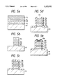
As shown in FIG. 5a, the surface of an n-Si(100) substrate 111 is cleaned, and an undoped single crystalline Si layer 112 with a thickness of 5 nm, a single crystalline Si0.8 Ge0.2 layer 113 with a thickness of 10 nm, and an undoped single crystalline Si layer 114 with a thickness of 5 nm are grown at 650° C. using the MBE (molecular beam epitaxy) method. The sample with the structure shown in FIG. 5a is taken from the molecular beam epitaxy apparatus. A p type hydrogenated amorphous Si layer 115 with a thickness of 100 nm is grown by the plasma CVD (chemical vapor deposition) method. Hydrogenated amorphous Si has wider band gap than Si, and an effect which is the same as that of Si1-B CB can be expected.
Thereafter, the structure shown in FIG. 5a is etched to a size of 4 μm (width) by 400 μm (length) by the dry etching method as shown in FIG. 5b. A SiO2 layer 116 with a thickness of 100 nm is deposited on it at 400° C. by the CVD method as shown in FIG. 5c. A hole is made in the SiO2 layer 116 by the photolithography method as shown in FIG. 5d. Al is deposited and patterned as shown in FIG. 5d so as to form electrodes 117 and 118 (FIG. 5e). A light emitting device of about 1 eV which emits light at room temperature is produced.
Even when three layers of the layered structure consisting of the undoped single crystalline Si layer 112 and single crystalline Si0.8 Ge0.2 layer 113 are formed in the same thickness as the above mentioned and the other layers are the same as the above mentioned, a light emitting device which emits light at room temperature is obtained. The light emitting efficiency in this case is about two times of the above mentioned.
Even if a p type hydrogenated amorphous Si0.9 C0.1 layer is used in place of the p type hydrogenated amorphous Si layer 115, a light emitting device which emits light almost in the same way is obtained.
Embodiment 3
As shown in FIG. 6a, the surface of an n-Si(100) substrate 121 is cleaned, and an n type single crystalline Si0.55 Ge0.40 C0.05 layer 122 with a thickness of 100 nm, an undoped single crystalline Si0.55 Ge0.40 C0.05 layer 123 with a thickness of 5 nm, a single crystalline Si0.8 Ge0.2 layer 124 with a thickness of 10 nm, an undoped single crystalline Si0.55 Ge0.40 C0.05 layer 125 with a thickness of 5 nm, and a p type single crystalline Si0.55 Ge0.40 C0.05 layer 126 with a thickness of 100 nm are grown at 650° C. by the MBE method.
Thereafter, the structure shown in FIG. 6a is processed in the shape shown in FIG. 6b by the dry etching method in the same way as with Embodiment 2. A SiO2 layer 127 with a thickness of 100 nm is deposited on it at 400° C. by the CVD method as shown in FIG. 6c. The structure shown in FIG. 6c is shaped as shown in FIG. 6d by the photolithography method. Al is deposited and patterned as shown in FIG. 6d so as to form electrodes 128 and 129 (FIG. 6e). A light emitting device of about 1 eV which emits light at room temperature is produced.
Even when three layers of the above mentioned layered structure consisting of the undoped single crystalline Si0.55 Ge0.40 C0.05 layer 123 and single crystalline Si0.8 Ge0.2 layer 124 are formed in the same thickness and the other layers are the same as the above mentioned, a light emitting device which emits light at room temperature is obtained. The light emitting efficiency in this case is about two times of the above mentioned.
Even if a p type single crystalline Si0.9 C0.1 layer is used in place of the p type single crystalline Si0.55 Ge0.40 C0.05 layer, a light emitting device which emits light almost in the same way is obtained.
Embodiment 4
As shown in FIG. 7a, the surface of an n-Si(100) substrate 131 is cleaned, and an n type single crystalline Si layer 132 with a thickness of 100 nm, an undoped single crystalline Si layer 133 with a thickness of 5 nm, a single crystalline Si0.8 Ge0.1 Sn0.1 layer 134 with a thickness of 10 nm, an undoped single crystalline Si layer 135 with a thickness of 5 nm, and a p type single crystalline Si layer 136 with a thickness of 100 nm are grown at 650° C. by the MBE method.
Thereafter, the structure shown in FIG. 7a is processed in the shape shown in FIG. 7b by the dry etching method in the same way as with Embodiment 2. A SiO2 layer 137 with a thickness of 100 nm is deposited on it at 400° C. by the CVD method as shown in FIG. 7c. The structure shown in FIG. 7c is shaped as shown in FIG. 7d by the photolithography method. Al is deposited and patterned as shown in FIG. 7d so as to form electrodes 138 and 139 (FIG. 7e). A light emitting device of about 1 eV which emits light at room temperature is produced.
Even when three layers of the layered structure consisting of the undoped single crystalline Si layer 133 and single crystalline Si0.8 Ge0.1 Sn0.1 layer 134 are formed in the same thickness as the above mentioned and the other layers are the same as the above mentioned, a light emitting device which emits light at room temperature is obtained. The light emitting efficiency in this case is about two times of the above mentioned.
Embodiment 5
An example that electronic elements are formed on the substrate on which the light emitting device shown in Embodiment 2 is formed, and an opto-electronic integrated circuit is formed will be explained hereunder. As shown in FIG. 8a, the surface of an Si(100) substrate 141 is cleaned, and a p type single crystalline Si layer 115' with a thickness of 100 nm is formed at 650° C. by the MBE method, and then an undoped single crystalline Si layer 114 with a thickness of 5 nm, a single crystalline Si0.8 Ge0.2 layer 113 with a thickness of 10 nm, and an undoped single crystalline Si layer 112 with a thickness of 5 nm are grown in the reverse order of that shown in Embodiment 2, and then an n type single crystalline Si layer 140 is formed.
Thereafter, as shown in FIG. 8b, the light emitting device in the light emitting portion, the electronic element for transferring electric signals to it, the light sensing device in the light sensing portion, and the electronic element for receiving electric signals from it are processed in the predetermined shapes by the dry etching method. The light emitting device portion and light sensing device portion are processed in the same way as with Embodiment 2 so as to form devices, and the electronic element portion is formed as an n type region 142 by ion implantation so as to form a field effect transistor using it as a source drain, and the circuit is wired as shown in the drawing. This opto-electronic integrated circuit operates satisfactorily at room temperature.
Even when three layers of the layered structures consisting of the undoped single crystalline Si layer and single crystalline Si0.8 Ge0.2 layer are formed in the same way as with Embodiment 2 and the other layers are the same as the above mentioned, an opto-electronic integrated circuit having an almost similar effect is obtained. According to the embodiment, a space is provided between the light emitting surface of the light emitting device and the light sensing surface of the light sensing device. However, an optical guide made of a transparent material such as glass may be mounted. The same may be said with the subsequent embodiments.
Embodiment 6
An example that electronic elements are formed on the substrate on which the light emitting device shown in Embodiment 3 is formed, and an opto-electronic integrated circuit is formed will be explained hereunder. The surface of an Si(100) substrate is cleaned and then the corresponding layers are formed in the reverse order of that in Embodiment 3 starting with a p type single crystalline Si0.55 Ge0.40 C0.05 layer. Next, each element portion is processed in the predetermined shape by the dry etching method according to Embodiment 5. By doing this, the elements and circuit lines are formed.
The obtained opto-electronic integrated circuit has a structure that the light emitting device and light sensing device of the structure shown in FIG. 8b are replaced with the devices shown in Embodiment 3 (the structure shown in Embodiment 3 is made upside down) and operates satisfactorily at room temperature.
Even when three layers of the layered structure consisting of the undoped single crystalline Si0.55 Ge0.40 C0.05 layer and single crystalline Si0.8 Ge0.2 layer are formed and the other layers are the same as the above mentioned and furthermore even when a p type single crystalline Si0.9 C0.1 layer is used in place of the p type single crystalline Si0.55 Ge0.40 C0.05 layer, an opto-electronic integrated circuit which has an almost similar effect is obtained.
Embodiment 7
An example where electronic elements are formed on the substrate on which the light emitting device shown in Embodiment 4 is formed, and an opto-electronic integrated circuit is formed will be explained hereunder. The surface of an Si(100) substrate is cleaned and then the corresponding layers are formed in the reverse order of that in Embodiment 4 starting with a p type single crystalline Si layer. Next, each element portion is processed in the predetermined shape by the dry etching method according to Embodiment 5. By doing this, the elements and circuit lines are formed.
The obtained opto-electronic integrated circuit has a structure that the light emitting device and light sensing device of the structure shown in FIG. 8b are replaced with the devices shown in Embodiment 4 (the structure shown in Embodiment 4 is made upside down) and operates satisfactorily at room temperature.
Even when three layers of the layered structure consisting of the undoped single crystalline Si layer and single crystalline Si0.8 Ge0.1 Sn0.1 layer are formed and the other layers are the same as the above mentioned and furthermore even when an undoped single crystalline Si0.9 Ge0.1 layer is used in place of the undoped single crystalline Si layer, or even when three layers of a layered structure consisting of this layer and a single crystalline Si0.8 Ge0.1 Sn0.1 layer are formed and furthermore even when an n type single crystalline Si0.9 Ge0.1 layer is used in place of the n type single crystalline Si layer or even when a p type single crystalline Si0.9 Ge0.1 layer is used in place of the p type single crystalline Si layer, an opto-electronic integrated circuit which has an almost similar effect is obtained.
Embodiment 8
The surface of a p-Si(100) substrate is cleaned, and then a p type Si0.7 Ge0.3 buffer layer with a thickness of 400 nm is formed, and an undoped Si0.7 Ge0.3 layer with a thickness of 100 nm is formed, and a layered structure consisting of an undoped Si0.9 Ge0.1 layer with a thickness of 5 nm and an updoped Si0.7 Ge0.3 layer with a thickness of 5 nm, an Si0.9 Ge0.1 layer with a thickness of 10 nm, and an n type Si0.9 Ge0.1 layer with a thickness of 40 nm are formed sequentially. Next, in the same way as with Embodiments 5 to 7, the light emitting device in the light emitting portion, the electronic element for transferring electric signals to it, the light sensing device in the light sensing portion, and the electronic element for receiving electric signals from it are processed in the predetermined shapes by the dry etching method. The light emitting device portion and light sensing device portion are processed in the same way as with Embodiment 1 so as to form devices, and the electronic element portion is formed as an n type region by ion implantation so as to form a field effect transistor using it as a source drain, and the circuit is wired as shown in FIG. 8b. This opto-electronic integrated circuit operates satisfactorily at room temperature. When the number of layered structures is increased, the efficiency of each of the light emitting device and light sensing device can be enhanced.
As shown by the above description, according to the present invention, since a light emitting device can be formed using IV-group semiconductors such as Si and Ge, not only LSIs but also optical devices can be formed on the same substrate. Therefore, light can be used easily in place of conventional circuit lines between LSIs.
The semiconductor optical device of the present invention operates at room temperature and a quantum efficiency of at least 1% is obtained.

Claims (24)

What is claimed is:
1. A semiconductor optical device comprising a first conductivity type single crystalline Si substrate, a first conductivity type buffer layer of Si1-X GeX which is formed on said single crystalline Si substrate, a layered structure consisting of at least one pair of an Si1-Y GeY layer and Si1-Z GeZ layer which are lattice-matched and formed alternately on said buffer layer, and a second conductivity type Si1-Y GeY layer which is formed on said layered structure, wherein X, Y, and Z satisfy the conditions that 0<X<0.5, 0<Y<0.5, 0<Z<0.5, Y<X, and Y<Z, and wherein said layered structure forms a light emitting region.
2. A semiconductor optical device according to claim 1, wherein the thicknesses of said Si1-Y GeY layer and said Si1-Z GeZ layer constituting said layered structure range from 5 nm to 10 nm.
3. A semiconductor optical device according to claim 2, wherein the thickness of said buffer layer is at least the critical film thickness.
4. A semiconductor optical device according to claim 1, wherein said layered structure comprises a plurality of pairs of Si1-Y GeY layers and said Si1-Z GeZ layers.
5. A semiconductor optical device comprising a first conductivity type single crystalline Si substrate, a layered structure consisting of at least one pair of an undoped single crystalline Si layer and single crystalline Si1-A GeA mixed crystal layer (0<A<1) which are lattice-matched and formed alternately on said single crystalline Si layer, a second undoped single crystalline Si layer which is mounted on said layered structure, and a second conductivity type Si1-B CB layer (0≦B<1) which is mounted on said second undoped single crystalline Si layer, wherein said Si1-B CB layer has a wider band gap than said second undoped single crystalline Si layer to form a potential barrier and, said single crystalline Si1-A GeA mixed crystal is a light emitting region.
6. A semiconductor optical device according to claim 5, wherein said first conductivity type single crystalline Si substrate is an n type single crystalline Si substrate and constitutes an electron injection electrode, and said second conductivity type Si1-B CB layer is a p type hydrogenated amorphous Si1-B CB layer and constitutes a hole injection electrode.
7. A semiconductor optical device according to claim 5, wherein the thicknesses of said Si1-A GeA mixed crystal layer and Si layer constituting said layered structure range from 2 nm to 20 nm and 2 nm to 10 nm respectively.
8. A semiconductor optical device according to claim 5, wherein said layered structure comprises a plurality of pairs of undoped single crystalline Si layers and single crystalline Si1-A GeA mixed crystal layers.
9. A semiconductor optical device comprising a first conductivity type single crystalline Si1-C-D GeC CD mixed crystal layer (0<C<1, 0<D<1), a layered structure consisting of at least one pair of an undoped single crystalline Si1-E-F GeE CF mixed crystal layer (0<E<1, 0<F<1) and a single crystalline Si1-G GeG mixed crystal layer (0<G<1) which are lattice-matched and formed alternately on said single crystalline Si1-C-D GeC CD mixed crystal layer, a second undoped single crystalline Si1-E-F GeE CF mixed crystal layer which is mounted on said layered structure, and a second conductivity type single crystalline Si1-H-I GeH C1 mixed crystal layer (0≦H<1, 0<I<1) which is mounted on said second undoped single crystalline Si1-E-F GeE CF mixed crystal layer, wherein said single crystalline Si1-G GeG mixed crystal layer is a light emitting region.
10. A semiconductor optical device according to claim 9, wherein said first conductivity type single crystalline Si1-C-D GeC CD mixed crystal layer is an n type single crystalline Si1-C-D GeC CD mixed crystal layer and constitutes an electron injection electrode and said second conductivity type single crystalline Si1-H-I GeH CI mixed crystal layer is a p type single crystalline Si1-H-I GeH CI mixed crystal layer and constitutes a hole injection electrode.
11. A semiconductor optical device according to claim 9, wherein the thicknesses of said Si1-E-F GeE CF mixed crystal layer and Si1-G GeG mixed crystal layer constituting said layered structure range from 2 nm to 10 nm and 2 nm to 20 nm respectively.
12. A semiconductor optical device according to claim 9, wherein said layered structure comprises a plurality of pairs of undoped single crystalline Si1-E-F GeE CF mixed crystal layers and single crystalline Si1-G GeG mixed crystal layers.
13. A semiconductor optical device comprising a first conductivity type single crystalline Si1-J GeJ mixed crystal layer (0≦J<1), a layered structure consisting of at least one pair of an undoped single crystalline Si1-K GeK mixed crystal layer (0≦K<1) and a single crystalline Si1-L-M GeL SnM mixed crystal layer (0<L<1, 0<M<1) which are lattice-matched and formed alternately on said single crystalline Si1-J GeJ mixed crystal layer, a second undoped single crystalline Si1-K GeK mixed crystal layer which is mounted on said layered structure, and a second conductivity type single crystalline Si1-N GeN mixed crystal layer (0<N<1) which is mounted on said second undoped single crystalline Si1-K GeK mixed crystal layer wherein said single crystalline Si1-L-M GeL SnM mixed crystal layer is a light emitting region.
14. A semiconductor optical device according to claim 13, wherein said first conductivity type single crystalline Si1-J GeJ mixed crystal layer is an n type single crystalline Si1-J GeJ mixed crystal layer and constitutes an electron injection electrode, and said second conductivity type single crystalline Si1-N GeN mixed crystal layer is a p type single crystalline Si1-N GeN mixed crystal layer and constitutes a hole injection electrode.
15. A semiconductor optical device according to claim 13, wherein the thicknesses of said Si1-K GeK mixed crystal layer and said Si1-L-M GeL SnM mixed crystal layer constituting said layered structure range from 2 nm to 10 nm and 2 nm to 20 nm respectively.
16. A semiconductor optical device according to claim 13, wherein said layered structure comprises a plurality of pairs of undoped single crystalline Si1-K GeK mixed crystal layers and single crystalline Si1-L-M GeL SnM mixed crystal layers.
17. An opto-electronic integrated circuit comprising a semiconductor optical device as claimed in claim 1 and electronic elements formed on said Si substrate.
18. An opto-electronic integrated circuit comprising a semiconductor optical device as claimed in claim 5 and electronic elements formed on said Si substrate.
19. An opto-electronic integrated circuit comprising a semiconductor optical device as claimed in claim 9, said device being mounted on a semiconductor substrate, and electronic elements formed on the semiconductor substrate on which said semiconductor optical device is mounted.
20. An opto-electronic integrated circuit comprising a semiconductor optical device as claimed in claim 13, said device being mounted on a semiconductor substrate, and electronic elements formed on the semiconductor substrate on which said semiconductor optical device is mounted.
21. An opto-electronic integrated circuit comprising:
(1) a light emitting portion having a light emitting device comprising a first semiconductor optical device as claimed in claim 1 and electronic elements formed on said Si substrate; and
(2) a light sensing portion having a light sensing device comprising a second semiconductor optical device which is formed on said Si substrate and other electronic elements formed on said semiconductor substrate, wherein the light emitting surface of said light emitting device and the light sensing surface of said light sensing device are arranged so that they are opposite to each other.
22. An opto-electronic integrated circuit comprising:
(1) a light emitting portion having a light emitting device comprising a first semiconductor optical device as claimed in claim 5 and electronic elements formed on said Si substrate; and
(2) a light sensing portion having a light sensing device comprising a second semiconductor optical device which is formed on said Si substrate and other electronic elements formed on said semiconductor substrate, wherein the light emitting surface of said light emitting device and the light sensing surface of said light sensing device are arranged so that they are opposite to each other.
23. An opto-electronic integrated circuit comprising:
(1) a light emitting portion having a light emitting device comprising a first semiconductor optical device as claimed in claim 9, said device being mounted on a semiconductor substrate, and electronic elements formed on the semiconductor substrate on which said light emitting device is mounted; and
(2) a light sensing portion having a light sensing device comprising a second semiconductor optical device which is formed on said semiconductor substrate and other electronic elements formed on said semiconductor substrate, wherein the light emitting surface of said light emitting device and the light sensing surface of said light sensing device are arranged so that they are opposite to each other.
24. An opto-electronic integrated circuit comprising:
(1) a light emitting portion having a light emitting device comprising a first semiconductor optical device as claimed in claim 13, said device being mounted on a semiconductor substrate, and electronic elements formed on the semiconductor substrate on which said light emitting device is mounted; and
(2) a light sensing portion having a light sensing device comprising a second semiconductor optical device which is formed on said semiconductor substrate and other electronic elements formed on said semiconductor substrate, wherein the light emitting surface of said light emitting device and the light sensing surface of said light sensing device are arranged so that they are opposite to each other.
US08/189,865 1993-02-03 1994-02-01 Semiconductor optical device, manufacturing method for the same, and opto-electronic integrated circuit using the same Expired - Fee Related US5523592A (en)

Applications Claiming Priority (4)

Application Number Priority Date Filing Date Title
JP5-016524 1993-02-03
JP1652493A JPH06232448A (en) 1993-02-03 1993-02-03 Light emitting element and optoelectronic integrated circuit
JP3963193A JPH06252441A (en) 1993-03-01 1993-03-01 Semiconductor optical device and manufacture thereof
JP5-039631 1993-03-01

Publications (1)

Publication Number Publication Date
US5523592A true US5523592A (en) 1996-06-04

Family

ID=26352877

Family Applications (1)

Application Number Title Priority Date Filing Date
US08/189,865 Expired - Fee Related US5523592A (en) 1993-02-03 1994-02-01 Semiconductor optical device, manufacturing method for the same, and opto-electronic integrated circuit using the same

Country Status (1)

Country Link
US (1) US5523592A (en)

Cited By (65)

* Cited by examiner, † Cited by third party
Publication number Priority date Publication date Assignee Title
EP0812023A1 (en) * 1996-04-09 1997-12-10 Max-Planck-Gesellschaft zur Förderung der Wissenschaften e.V. Semiconductor components, in particular photodetectors, light emitting diodes, optical modulators and waveguides with multilayer structures grown on silicon substrates
WO1998052230A2 (en) * 1997-05-16 1998-11-19 Koninklijke Philips Electronics N.V. Silicongermanium semiconductor device and a method of manufacturing the same
US5942792A (en) * 1997-05-02 1999-08-24 Nec Corporation Compound semiconductor device having a multilayer silicon structure between an active region and insulator layer for reducing surface state density at interface
US6154475A (en) * 1997-12-04 2000-11-28 The United States Of America As Represented By The Secretary Of The Air Force Silicon-based strain-symmetrized GE-SI quantum lasers
US6350993B1 (en) * 1999-03-12 2002-02-26 International Business Machines Corporation High speed composite p-channel Si/SiGe heterostructure for field effect devices
US6399970B2 (en) * 1996-09-17 2002-06-04 Matsushita Electric Industrial Co., Ltd. FET having a Si/SiGeC heterojunction channel
US6403975B1 (en) 1996-04-09 2002-06-11 Max-Planck Gesellschaft Zur Forderung Der Wissenschafteneev Semiconductor components, in particular photodetectors, light emitting diodes, optical modulators and waveguides with multilayer structures grown on silicon substrates
US20020084000A1 (en) * 1997-06-24 2002-07-04 Eugene A. Fitzgerald Controlling threading dislocation densities in Ge on Si using graded GeSi layers and planarization
US20020123167A1 (en) * 2001-03-02 2002-09-05 Fitzgerald Eugene A. Relaxed silicon germanium platform for high speed CMOS electronics and high speed analog circuits
US20020197803A1 (en) * 2001-06-21 2002-12-26 Amberwave Systems Corporation Enhancement of p-type metal-oxide-semiconductor field effect transistors
US20030013323A1 (en) * 2001-06-14 2003-01-16 Richard Hammond Method of selective removal of SiGe alloys
US6537369B1 (en) * 2000-03-27 2003-03-25 Matsushita Electric Industrial Co., Ltd. SiGeC semiconductor crystal and production method thereof
US20030057439A1 (en) * 2001-08-09 2003-03-27 Fitzgerald Eugene A. Dual layer CMOS devices
US20030077867A1 (en) * 2001-03-02 2003-04-24 Fitzergald Eugene A. Relaxed silicon germanium platform for high speed CMOS electronics and high speed analog circuits
US6555839B2 (en) 2000-05-26 2003-04-29 Amberwave Systems Corporation Buried channel strained silicon FET using a supply layer created through ion implantation
US6573126B2 (en) 2000-08-16 2003-06-03 Massachusetts Institute Of Technology Process for producing semiconductor article using graded epitaxial growth
US20030102498A1 (en) * 2001-09-24 2003-06-05 Glyn Braithwaite RF circuits including transistors having strained material layers
US20030113948A1 (en) * 2000-01-20 2003-06-19 Amberwave Systems Corporation Low threading dislocation density relaxed mismatched epilayers without high temperature growth
US6593641B1 (en) 2001-03-02 2003-07-15 Amberwave Systems Corporation Relaxed silicon germanium platform for high speed CMOS electronics and high speed analog circuits
US6602613B1 (en) 2000-01-20 2003-08-05 Amberwave Systems Corporation Heterointegration of materials using deposition and bonding
WO2003069652A2 (en) * 2002-02-13 2003-08-21 The Regents Of The University Of California A multilayer structure to form an active matrix display having single crystalline drivers over a transmissive substrate
US20030157917A1 (en) * 2002-02-15 2003-08-21 Shahla Khorram Programmable mixer and radio applications thereof
US6646322B2 (en) * 2001-03-02 2003-11-11 Amberwave Systems Corporation Relaxed silicon germanium platform for high speed CMOS electronics and high speed analog circuits
US6649480B2 (en) 2000-12-04 2003-11-18 Amberwave Systems Corporation Method of fabricating CMOS inverter and integrated circuits utilizing strained silicon surface channel MOSFETs
US20030215990A1 (en) * 2002-03-14 2003-11-20 Eugene Fitzgerald Methods for fabricating strained layers on semiconductor substrates
US6667489B2 (en) * 2001-11-29 2003-12-23 Hitachi, Ltd. Heterojunction bipolar transistor and method for production thereof
US20040000268A1 (en) * 1998-04-10 2004-01-01 Massachusetts Institute Of Technology Etch stop layer system
US20040026765A1 (en) * 2002-06-07 2004-02-12 Amberwave Systems Corporation Semiconductor devices having strained dual channel layers
US20040040493A1 (en) * 2002-08-30 2004-03-04 Amberwave Systems Corporation Reduction of dislocation pile-up formation during relaxed lattice-mismatched epitaxy
US6703688B1 (en) 2001-03-02 2004-03-09 Amberwave Systems Corporation Relaxed silicon germanium platform for high speed CMOS electronics and high speed analog circuits
US6724008B2 (en) 2001-03-02 2004-04-20 Amberwave Systems Corporation Relaxed silicon germanium platform for high speed CMOS electronics and high speed analog circuits
US20040075149A1 (en) * 2000-12-04 2004-04-22 Amberwave Systems Corporation CMOS inverter and integrated circuits utilizing strained silicon surface channel MOSFETs
US6730551B2 (en) 2001-08-06 2004-05-04 Massachusetts Institute Of Technology Formation of planar strained layers
US20040092085A1 (en) * 2001-01-31 2004-05-13 Yoshihiko Kanzawa Semiconductor crystal film and method for preparation thereof
US6750130B1 (en) 2000-01-20 2004-06-15 Amberwave Systems Corporation Heterointegration of materials using deposition and bonding
US6787793B2 (en) * 2001-12-11 2004-09-07 Sharp Kabushiki Kaisha Strained Si device with first SiGe layer with higher Ge concentration being relaxed to have substantially same lattice constant as second SiGe layer with lower Ge concentration
US20050023554A1 (en) * 1998-03-02 2005-02-03 International Business Machines Corporation Si/SiGe optoelectronic integrated circuits
US20050054168A1 (en) * 2001-09-21 2005-03-10 Amberwave Systems Corporation Semiconductor structures employing strained material layers with defined impurity gradients and methods for fabricating same
US6888175B1 (en) 1998-05-29 2005-05-03 Massachusetts Institute Of Technology Compound semiconductor structure with lattice and polarity matched heteroepitaxial layers
US6897471B1 (en) * 2003-11-28 2005-05-24 The United States Of America As Represented By The Secretary Of The Air Force Strain-engineered direct-gap Ge/SnxGe1-x heterodiode and multi-quantum-well photodetectors, laser, emitters and modulators grown on SnySizGe1-y-z-buffered silicon
US6900103B2 (en) 2001-03-02 2005-05-31 Amberwave Systems Corporation Relaxed silicon germanium platform for high speed CMOS electronics and high speed analog circuits
US6940089B2 (en) 2001-04-04 2005-09-06 Massachusetts Institute Of Technology Semiconductor device structure
US6995430B2 (en) 2002-06-07 2006-02-07 Amberwave Systems Corporation Strained-semiconductor-on-insulator device structures
US7074623B2 (en) 2002-06-07 2006-07-11 Amberwave Systems Corporation Methods of forming strained-semiconductor-on-insulator finFET device structures
WO2006085361A1 (en) * 2005-02-09 2006-08-17 Fujitsu Limited Light-emitting device and semiconductor device
US7122449B2 (en) 2002-06-10 2006-10-17 Amberwave Systems Corporation Methods of fabricating semiconductor structures having epitaxially grown source and drain elements
US7138649B2 (en) 2001-08-09 2006-11-21 Amberwave Systems Corporation Dual-channel CMOS transistors with differentially strained channels
US20070082470A1 (en) * 2000-08-07 2007-04-12 Amberwave System Corporation Gate technology for strained surface channel and strained buried channel MOSFET devices
US7217603B2 (en) 2002-06-25 2007-05-15 Amberwave Systems Corporation Methods of forming reacted conductive gate electrodes
US7301180B2 (en) 2001-06-18 2007-11-27 Massachusetts Institute Of Technology Structure and method for a high-speed semiconductor device having a Ge channel layer
US7307273B2 (en) 2002-06-07 2007-12-11 Amberwave Systems Corporation Control of strain in device layers by selective relaxation
US7332417B2 (en) 2003-01-27 2008-02-19 Amberwave Systems Corporation Semiconductor structures with structural homogeneity
US7335545B2 (en) 2002-06-07 2008-02-26 Amberwave Systems Corporation Control of strain in device layers by prevention of relaxation
US7368308B2 (en) 2002-08-23 2008-05-06 Amberwave Systems Corporation Methods of fabricating semiconductor heterostructures
US20080128713A1 (en) * 2006-04-25 2008-06-05 Shinichi Saito Silicon light emitting diode, silicon optical transistor, silicon laser and its manufacturing method
US7393733B2 (en) 2004-12-01 2008-07-01 Amberwave Systems Corporation Methods of forming hybrid fin field-effect transistor structures
US20090016666A1 (en) * 2004-12-09 2009-01-15 Yu-Hsuan Kuo Silicon-based ge/sige optical interconnects
US7504704B2 (en) 2003-03-07 2009-03-17 Amberwave Systems Corporation Shallow trench isolation process
US7515776B1 (en) * 2004-12-09 2009-04-07 The Board Of Trustees Of The Leland Stanford Junior University Temperature-controlled optical modulator
WO2009095886A3 (en) * 2008-02-01 2009-09-24 Insiava (Pty) Limited Semiconductor light emitting device comprising heterojunction
US7615829B2 (en) 2002-06-07 2009-11-10 Amberwave Systems Corporation Elevated source and drain elements for strained-channel heterojuntion field-effect transistors
US20100254425A1 (en) * 2007-06-29 2010-10-07 International Business Machines Corporation Phase change material based temperature sensor
WO2011037574A1 (en) * 2009-09-25 2011-03-31 Hewlett-Packard Development Company, L.P. Silicon-germanium, quantum-well, light-emitting diode
US20140077240A1 (en) * 2012-09-17 2014-03-20 Radek Roucka Iv material photonic device on dbr
US8748292B2 (en) 2002-06-07 2014-06-10 Taiwan Semiconductor Manufacturing Company, Ltd. Methods of forming strained-semiconductor-on-insulator device structures

Citations (8)

* Cited by examiner, † Cited by third party
Publication number Priority date Publication date Assignee Title
US4527179A (en) * 1981-02-09 1985-07-02 Semiconductor Energy Laboratory Co., Ltd. Non-single-crystal light emitting semiconductor device
JPS63108782A (en) * 1986-10-27 1988-05-13 Nec Corp Semiconductor photodetector
US4772924A (en) * 1985-11-18 1988-09-20 Bean John C Device having strain induced region of altered bandgap
US4843028A (en) * 1985-05-17 1989-06-27 Icentia Patent-Verwaltungs-Gmbh Method for producing a spatially periodic semiconductor layer structure
US4927471A (en) * 1988-03-01 1990-05-22 Fujitsu Limited Semiconductor substrate comprising wafer substrate and compound semiconductor layer
US5014096A (en) * 1989-02-09 1991-05-07 Matsushita Electric Industrial Co., Ltd. Optoelectronic integrated circuit with optical gate device and phototransistor
US5057880A (en) * 1989-10-23 1991-10-15 Fujitsu Limited Semiconductor device having a heteroepitaxial substrate
US5272548A (en) * 1989-06-07 1993-12-21 Canon Kabushiki Kaisha Photosensor and image reading device with improved correction means for signal correction and image reading method

Patent Citations (8)

* Cited by examiner, † Cited by third party
Publication number Priority date Publication date Assignee Title
US4527179A (en) * 1981-02-09 1985-07-02 Semiconductor Energy Laboratory Co., Ltd. Non-single-crystal light emitting semiconductor device
US4843028A (en) * 1985-05-17 1989-06-27 Icentia Patent-Verwaltungs-Gmbh Method for producing a spatially periodic semiconductor layer structure
US4772924A (en) * 1985-11-18 1988-09-20 Bean John C Device having strain induced region of altered bandgap
JPS63108782A (en) * 1986-10-27 1988-05-13 Nec Corp Semiconductor photodetector
US4927471A (en) * 1988-03-01 1990-05-22 Fujitsu Limited Semiconductor substrate comprising wafer substrate and compound semiconductor layer
US5014096A (en) * 1989-02-09 1991-05-07 Matsushita Electric Industrial Co., Ltd. Optoelectronic integrated circuit with optical gate device and phototransistor
US5272548A (en) * 1989-06-07 1993-12-21 Canon Kabushiki Kaisha Photosensor and image reading device with improved correction means for signal correction and image reading method
US5057880A (en) * 1989-10-23 1991-10-15 Fujitsu Limited Semiconductor device having a heteroepitaxial substrate

Non-Patent Citations (6)

* Cited by examiner, † Cited by third party
Title
Appl. Phys. Lett. 60 (14). Apr. 6, 1992, "Photoluminescence from electron-hole plasmas confined in Si/Si1-x Gex /Si quantum wells", Xiao, C. W. Liu, et al.
Appl. Phys. Lett. 60 (14). Apr. 6, 1992, Photoluminescence from electron hole plasmas confined in Si/Si 1 x Ge x /Si quantum wells , Xiao, C. W. Liu, et al. *
Mi, et al IEEE Trans. on Elec. Dev., vol. 39 No. 11 Nov. 92, "Room-Temp, on Si/Si1-x Gex Quantum Wells".
Mi, et al IEEE Trans. on Elec. Dev., vol. 39 No. 11 Nov. 92, Room Temp, on Si/Si 1 x Ge x Quantum Wells . *
Physical Review Letters, vol. 66, No. 10, "Well-Resolved Band-Edge Photoluminescence of Excitons Confined in Strained Si1-x Gex Quantum Wells", J. C. Sturm, et al.
Physical Review Letters, vol. 66, No. 10, Well Resolved Band Edge Photoluminescence of Excitons Confined in Strained Si 1 x Ge x Quantum Wells , J. C. Sturm, et al. *

Cited By (146)

* Cited by examiner, † Cited by third party
Publication number Priority date Publication date Assignee Title
EP0812023A1 (en) * 1996-04-09 1997-12-10 Max-Planck-Gesellschaft zur Förderung der Wissenschaften e.V. Semiconductor components, in particular photodetectors, light emitting diodes, optical modulators and waveguides with multilayer structures grown on silicon substrates
US6403975B1 (en) 1996-04-09 2002-06-11 Max-Planck Gesellschaft Zur Forderung Der Wissenschafteneev Semiconductor components, in particular photodetectors, light emitting diodes, optical modulators and waveguides with multilayer structures grown on silicon substrates
US6399970B2 (en) * 1996-09-17 2002-06-04 Matsushita Electric Industrial Co., Ltd. FET having a Si/SiGeC heterojunction channel
US6674100B2 (en) 1996-09-17 2004-01-06 Matsushita Electric Industrial Co., Ltd. SiGeC-based CMOSFET with separate heterojunctions
US5942792A (en) * 1997-05-02 1999-08-24 Nec Corporation Compound semiconductor device having a multilayer silicon structure between an active region and insulator layer for reducing surface state density at interface
WO1998052230A3 (en) * 1997-05-16 1999-02-18 Koninkl Philips Electronics Nv Silicongermanium semiconductor device and a method of manufacturing the same
US6242762B1 (en) 1997-05-16 2001-06-05 U.S. Philips Corporation Semiconductor device with a tunnel diode and method of manufacturing same
WO1998052230A2 (en) * 1997-05-16 1998-11-19 Koninklijke Philips Electronics N.V. Silicongermanium semiconductor device and a method of manufacturing the same
US20040262631A1 (en) * 1997-06-24 2004-12-30 Massachusetts Institute Of Technology Controlling threading dislocation densities in Ge on Si using graded GeSi layers and planarization
US6876010B1 (en) 1997-06-24 2005-04-05 Massachusetts Institute Of Technology Controlling threading dislocation densities in Ge on Si using graded GeSi layers and planarization
US7250359B2 (en) 1997-06-24 2007-07-31 Massachusetts Institute Of Technology Controlling threading dislocation densities in Ge on Si using graded GeSi layers and planarization
US7081410B2 (en) 1997-06-24 2006-07-25 Massachusetts Institute Of Technology Controlling threading dislocation densities in Ge on Si using graded GeSi layers and planarization
US20020084000A1 (en) * 1997-06-24 2002-07-04 Eugene A. Fitzgerald Controlling threading dislocation densities in Ge on Si using graded GeSi layers and planarization
US6154475A (en) * 1997-12-04 2000-11-28 The United States Of America As Represented By The Secretary Of The Air Force Silicon-based strain-symmetrized GE-SI quantum lasers
US20050023554A1 (en) * 1998-03-02 2005-02-03 International Business Machines Corporation Si/SiGe optoelectronic integrated circuits
US7083998B2 (en) * 1998-03-02 2006-08-01 International Business Machines Corporation Si/SiGe optoelectronic integrated circuits
US7227176B2 (en) 1998-04-10 2007-06-05 Massachusetts Institute Of Technology Etch stop layer system
US20040000268A1 (en) * 1998-04-10 2004-01-01 Massachusetts Institute Of Technology Etch stop layer system
US6888175B1 (en) 1998-05-29 2005-05-03 Massachusetts Institute Of Technology Compound semiconductor structure with lattice and polarity matched heteroepitaxial layers
US6350993B1 (en) * 1999-03-12 2002-02-26 International Business Machines Corporation High speed composite p-channel Si/SiGe heterostructure for field effect devices
US6858502B2 (en) 1999-03-12 2005-02-22 International Business Machines Corporation High speed composite p-channel Si/SiGe heterostructure for field effect devices
US6750130B1 (en) 2000-01-20 2004-06-15 Amberwave Systems Corporation Heterointegration of materials using deposition and bonding
US6602613B1 (en) 2000-01-20 2003-08-05 Amberwave Systems Corporation Heterointegration of materials using deposition and bonding
US6703144B2 (en) 2000-01-20 2004-03-09 Amberwave Systems Corporation Heterointegration of materials using deposition and bonding
US20030113948A1 (en) * 2000-01-20 2003-06-19 Amberwave Systems Corporation Low threading dislocation density relaxed mismatched epilayers without high temperature growth
US6864115B2 (en) 2000-01-20 2005-03-08 Amberwave Systems Corporation Low threading dislocation density relaxed mismatched epilayers without high temperature growth
US6660393B2 (en) 2000-03-27 2003-12-09 Matsushita Electric Industrial Co., Ltd. SiGeC semiconductor crystals and the method producing the same
US6537369B1 (en) * 2000-03-27 2003-03-25 Matsushita Electric Industrial Co., Ltd. SiGeC semiconductor crystal and production method thereof
US20060011983A1 (en) * 2000-05-26 2006-01-19 Amberwave Systems Corporation Methods of fabricating strained-channel FET having a dopant supply region
US6555839B2 (en) 2000-05-26 2003-04-29 Amberwave Systems Corporation Buried channel strained silicon FET using a supply layer created through ion implantation
US20070082470A1 (en) * 2000-08-07 2007-04-12 Amberwave System Corporation Gate technology for strained surface channel and strained buried channel MOSFET devices
US6921914B2 (en) 2000-08-16 2005-07-26 Massachusetts Institute Of Technology Process for producing semiconductor article using graded epitaxial growth
US6573126B2 (en) 2000-08-16 2003-06-03 Massachusetts Institute Of Technology Process for producing semiconductor article using graded epitaxial growth
US20030168654A1 (en) * 2000-08-16 2003-09-11 Massachusetts Institute Of Technology Process for producing semiconductor article using graded epitaxial growth
US6713326B2 (en) 2000-08-16 2004-03-30 Masachusetts Institute Of Technology Process for producing semiconductor article using graded epitaxial growth
US6737670B2 (en) 2000-08-16 2004-05-18 Massachusetts Institute Of Technology Semiconductor substrate structure
US6649480B2 (en) 2000-12-04 2003-11-18 Amberwave Systems Corporation Method of fabricating CMOS inverter and integrated circuits utilizing strained silicon surface channel MOSFETs
US6881632B2 (en) 2000-12-04 2005-04-19 Amberwave Systems Corporation Method of fabricating CMOS inverter and integrated circuits utilizing strained surface channel MOSFETS
US20040075149A1 (en) * 2000-12-04 2004-04-22 Amberwave Systems Corporation CMOS inverter and integrated circuits utilizing strained silicon surface channel MOSFETs
US6852602B2 (en) * 2001-01-31 2005-02-08 Matsushita Electric Industrial Co., Ltd. Semiconductor crystal film and method for preparation thereof
US20040092085A1 (en) * 2001-01-31 2004-05-13 Yoshihiko Kanzawa Semiconductor crystal film and method for preparation thereof
US7501351B2 (en) 2001-03-02 2009-03-10 Amberwave Systems Corporation Relaxed SiGe platform for high speed CMOS electronics and high speed analog circuits
US8822282B2 (en) 2001-03-02 2014-09-02 Taiwan Semiconductor Manufacturing Company, Ltd. Methods of fabricating contact regions for FET incorporating SiGe
US20020123167A1 (en) * 2001-03-02 2002-09-05 Fitzgerald Eugene A. Relaxed silicon germanium platform for high speed CMOS electronics and high speed analog circuits
US6723661B2 (en) 2001-03-02 2004-04-20 Amberwave Systems Corporation Relaxed silicon germanium platform for high speed CMOS electronics and high speed analog circuits
US6900103B2 (en) 2001-03-02 2005-05-31 Amberwave Systems Corporation Relaxed silicon germanium platform for high speed CMOS electronics and high speed analog circuits
US20030077867A1 (en) * 2001-03-02 2003-04-24 Fitzergald Eugene A. Relaxed silicon germanium platform for high speed CMOS electronics and high speed analog circuits
US7256142B2 (en) 2001-03-02 2007-08-14 Amberwave Systems Corporation Relaxed SiGe platform for high speed CMOS electronics and high speed analog circuits
US6830976B2 (en) 2001-03-02 2004-12-14 Amberwave Systems Corproation Relaxed silicon germanium platform for high speed CMOS electronics and high speed analog circuits
US6724008B2 (en) 2001-03-02 2004-04-20 Amberwave Systems Corporation Relaxed silicon germanium platform for high speed CMOS electronics and high speed analog circuits
US6703688B1 (en) 2001-03-02 2004-03-09 Amberwave Systems Corporation Relaxed silicon germanium platform for high speed CMOS electronics and high speed analog circuits
US6593641B1 (en) 2001-03-02 2003-07-15 Amberwave Systems Corporation Relaxed silicon germanium platform for high speed CMOS electronics and high speed analog circuits
US6646322B2 (en) * 2001-03-02 2003-11-11 Amberwave Systems Corporation Relaxed silicon germanium platform for high speed CMOS electronics and high speed analog circuits
US6940089B2 (en) 2001-04-04 2005-09-06 Massachusetts Institute Of Technology Semiconductor device structure
US7348259B2 (en) 2001-04-04 2008-03-25 Massachusetts Institute Of Technology Method of fabricating a semiconductor structure that includes transferring one or more material layers to a substrate and smoothing an exposed surface of at least one of the material layers
US6900094B2 (en) 2001-06-14 2005-05-31 Amberwave Systems Corporation Method of selective removal of SiGe alloys
US20040171223A1 (en) * 2001-06-14 2004-09-02 Amberwave Systems Corporation Method of selective removal of SiGe alloys
US20030013323A1 (en) * 2001-06-14 2003-01-16 Richard Hammond Method of selective removal of SiGe alloys
US8436336B2 (en) 2001-06-18 2013-05-07 Massachusetts Institute Of Technology Structure and method for a high-speed semiconductor device having a Ge channel layer
US7301180B2 (en) 2001-06-18 2007-11-27 Massachusetts Institute Of Technology Structure and method for a high-speed semiconductor device having a Ge channel layer
US6916727B2 (en) 2001-06-21 2005-07-12 Massachusetts Institute Of Technology Enhancement of P-type metal-oxide-semiconductor field effect transistors
US20050151164A1 (en) * 2001-06-21 2005-07-14 Amberwave Systems Corporation Enhancement of p-type metal-oxide-semiconductor field effect transistors
US20020197803A1 (en) * 2001-06-21 2002-12-26 Amberwave Systems Corporation Enhancement of p-type metal-oxide-semiconductor field effect transistors
US20040164318A1 (en) * 2001-08-06 2004-08-26 Massachusetts Institute Of Technology Structures with planar strained layers
US20070072354A1 (en) * 2001-08-06 2007-03-29 Massachusetts Institute Of Technology Structures with planar strained layers
US7141820B2 (en) 2001-08-06 2006-11-28 Amberwave Systems Corporation Structures with planar strained layers
US6730551B2 (en) 2001-08-06 2004-05-04 Massachusetts Institute Of Technology Formation of planar strained layers
US20050221550A1 (en) * 2001-08-09 2005-10-06 Amberwave Systems Corporation Dual layer semiconductor devices
US6974735B2 (en) 2001-08-09 2005-12-13 Amberwave Systems Corporation Dual layer Semiconductor Devices
US20030057439A1 (en) * 2001-08-09 2003-03-27 Fitzgerald Eugene A. Dual layer CMOS devices
US20060266997A1 (en) * 2001-08-09 2006-11-30 Amberwave Systems Corporation Methods for forming semiconductor structures with differential surface layer thicknesses
US7138649B2 (en) 2001-08-09 2006-11-21 Amberwave Systems Corporation Dual-channel CMOS transistors with differentially strained channels
US7465619B2 (en) 2001-08-09 2008-12-16 Amberwave Systems Corporation Methods of fabricating dual layer semiconductor devices
US7884353B2 (en) 2001-09-21 2011-02-08 Taiwan Semiconductor Manufacturing Company, Ltd. Semiconductor structures employing strained material layers with defined impurity gradients and methods for fabricating same
US20050054168A1 (en) * 2001-09-21 2005-03-10 Amberwave Systems Corporation Semiconductor structures employing strained material layers with defined impurity gradients and methods for fabricating same
US20070293003A1 (en) * 2001-09-21 2007-12-20 Matthew Currie Semiconductor structures employing strained material layers with defined impurity gradients and methods for fabricating same
US7846802B2 (en) 2001-09-21 2010-12-07 Taiwan Semiconductor Manufacturing Company, Ltd. Semiconductor structures employing strained material layers with defined impurity gradients and methods for fabricating same
US7776697B2 (en) 2001-09-21 2010-08-17 Taiwan Semiconductor Manufacturing Company, Ltd. Semiconductor structures employing strained material layers with defined impurity gradients and methods for fabricating same
US7906776B2 (en) 2001-09-24 2011-03-15 Taiwan Semiconductor Manufacturing Company, Ltd. RF circuits including transistors having strained material layers
US7709828B2 (en) 2001-09-24 2010-05-04 Taiwan Semiconductor Manufacturing Company, Ltd. RF circuits including transistors having strained material layers
US20030102498A1 (en) * 2001-09-24 2003-06-05 Glyn Braithwaite RF circuits including transistors having strained material layers
US6933518B2 (en) 2001-09-24 2005-08-23 Amberwave Systems Corporation RF circuits including transistors having strained material layers
US6667489B2 (en) * 2001-11-29 2003-12-23 Hitachi, Ltd. Heterojunction bipolar transistor and method for production thereof
US6787793B2 (en) * 2001-12-11 2004-09-07 Sharp Kabushiki Kaisha Strained Si device with first SiGe layer with higher Ge concentration being relaxed to have substantially same lattice constant as second SiGe layer with lower Ge concentration
WO2003069652A3 (en) * 2002-02-13 2004-06-10 Univ California A multilayer structure to form an active matrix display having single crystalline drivers over a transmissive substrate
US20050140283A1 (en) * 2002-02-13 2005-06-30 Lau Silvanus S. Multilayer structure to form an active matrix display having single crystalline drivers over a transmissive substrate
WO2003069652A2 (en) * 2002-02-13 2003-08-21 The Regents Of The University Of California A multilayer structure to form an active matrix display having single crystalline drivers over a transmissive substrate
US20030157917A1 (en) * 2002-02-15 2003-08-21 Shahla Khorram Programmable mixer and radio applications thereof
US7060632B2 (en) 2002-03-14 2006-06-13 Amberwave Systems Corporation Methods for fabricating strained layers on semiconductor substrates
US20030215990A1 (en) * 2002-03-14 2003-11-20 Eugene Fitzgerald Methods for fabricating strained layers on semiconductor substrates
US7259108B2 (en) 2002-03-14 2007-08-21 Amberwave Systems Corporation Methods for fabricating strained layers on semiconductor substrates
US7414259B2 (en) 2002-06-07 2008-08-19 Amberwave Systems Corporation Strained germanium-on-insulator device structures
US7615829B2 (en) 2002-06-07 2009-11-10 Amberwave Systems Corporation Elevated source and drain elements for strained-channel heterojuntion field-effect transistors
US7420201B2 (en) 2002-06-07 2008-09-02 Amberwave Systems Corporation Strained-semiconductor-on-insulator device structures with elevated source/drain regions
US20070032009A1 (en) * 2002-06-07 2007-02-08 Amberwave Systems Corporation Semiconductor devices having strained dual channel layers
US7297612B2 (en) 2002-06-07 2007-11-20 Amberwave Systems Corporation Methods for forming strained-semiconductor-on-insulator device structures by use of cleave planes
US7074623B2 (en) 2002-06-07 2006-07-11 Amberwave Systems Corporation Methods of forming strained-semiconductor-on-insulator finFET device structures
US7335545B2 (en) 2002-06-07 2008-02-26 Amberwave Systems Corporation Control of strain in device layers by prevention of relaxation
US7138310B2 (en) 2002-06-07 2006-11-21 Amberwave Systems Corporation Semiconductor devices having strained dual channel layers
US7588994B2 (en) 2002-06-07 2009-09-15 Amberwave Systems Corporation Methods for forming strained-semiconductor-on-insulator device structures by mechanically inducing strain
US7838392B2 (en) 2002-06-07 2010-11-23 Taiwan Semiconductor Manufacturing Company, Ltd. Methods for forming III-V semiconductor device structures
US8748292B2 (en) 2002-06-07 2014-06-10 Taiwan Semiconductor Manufacturing Company, Ltd. Methods of forming strained-semiconductor-on-insulator device structures
US7566606B2 (en) 2002-06-07 2009-07-28 Amberwave Systems Corporation Methods of fabricating semiconductor devices having strained dual channel layers
US20040026765A1 (en) * 2002-06-07 2004-02-12 Amberwave Systems Corporation Semiconductor devices having strained dual channel layers
US7259388B2 (en) 2002-06-07 2007-08-21 Amberwave Systems Corporation Strained-semiconductor-on-insulator device structures
US6995430B2 (en) 2002-06-07 2006-02-07 Amberwave Systems Corporation Strained-semiconductor-on-insulator device structures
US7307273B2 (en) 2002-06-07 2007-12-11 Amberwave Systems Corporation Control of strain in device layers by selective relaxation
US7109516B2 (en) 2002-06-07 2006-09-19 Amberwave Systems Corporation Strained-semiconductor-on-insulator finFET device structures
US7122449B2 (en) 2002-06-10 2006-10-17 Amberwave Systems Corporation Methods of fabricating semiconductor structures having epitaxially grown source and drain elements
US7439164B2 (en) 2002-06-10 2008-10-21 Amberwave Systems Corporation Methods of fabricating semiconductor structures having epitaxially grown source and drain elements
US8129821B2 (en) 2002-06-25 2012-03-06 Taiwan Semiconductor Manufacturing Co., Ltd. Reacted conductive gate electrodes
US7217603B2 (en) 2002-06-25 2007-05-15 Amberwave Systems Corporation Methods of forming reacted conductive gate electrodes
US7368308B2 (en) 2002-08-23 2008-05-06 Amberwave Systems Corporation Methods of fabricating semiconductor heterostructures
US7829442B2 (en) 2002-08-23 2010-11-09 Taiwan Semiconductor Manufacturing Company, Ltd. Semiconductor heterostructures having reduced dislocation pile-ups and related methods
US7375385B2 (en) 2002-08-23 2008-05-20 Amberwave Systems Corporation Semiconductor heterostructures having reduced dislocation pile-ups
US20040040493A1 (en) * 2002-08-30 2004-03-04 Amberwave Systems Corporation Reduction of dislocation pile-up formation during relaxed lattice-mismatched epitaxy
US7594967B2 (en) 2002-08-30 2009-09-29 Amberwave Systems Corporation Reduction of dislocation pile-up formation during relaxed lattice-mismatched epitaxy
US20080135830A1 (en) * 2003-01-27 2008-06-12 Amberwave Systems Corporation Semiconductor structures with structural homogeneity
US7332417B2 (en) 2003-01-27 2008-02-19 Amberwave Systems Corporation Semiconductor structures with structural homogeneity
US7504704B2 (en) 2003-03-07 2009-03-17 Amberwave Systems Corporation Shallow trench isolation process
US6897471B1 (en) * 2003-11-28 2005-05-24 The United States Of America As Represented By The Secretary Of The Air Force Strain-engineered direct-gap Ge/SnxGe1-x heterodiode and multi-quantum-well photodetectors, laser, emitters and modulators grown on SnySizGe1-y-z-buffered silicon
US7393733B2 (en) 2004-12-01 2008-07-01 Amberwave Systems Corporation Methods of forming hybrid fin field-effect transistor structures
US8183627B2 (en) 2004-12-01 2012-05-22 Taiwan Semiconductor Manufacturing Company, Ltd. Hybrid fin field-effect transistor structures and related methods
US7515777B2 (en) * 2004-12-09 2009-04-07 The Board Of Trustees Of The Leland Stanford Junior University Silicon-based Ge/SiGe optical interconnects
US7515776B1 (en) * 2004-12-09 2009-04-07 The Board Of Trustees Of The Leland Stanford Junior University Temperature-controlled optical modulator
US20090016666A1 (en) * 2004-12-09 2009-01-15 Yu-Hsuan Kuo Silicon-based ge/sige optical interconnects
US7732823B2 (en) 2005-02-09 2010-06-08 Fujitsu Limited Light emitting device and semiconductor device
WO2006085361A1 (en) * 2005-02-09 2006-08-17 Fujitsu Limited Light-emitting device and semiconductor device
US20080006817A1 (en) * 2005-02-09 2008-01-10 Fujitsu Limited Light emitting device and semiconductor device
JP4612671B2 (en) * 2005-02-09 2011-01-12 富士通株式会社 Light emitting device and semiconductor device
JPWO2006085361A1 (en) * 2005-02-09 2008-06-26 富士通株式会社 Light emitting device and semiconductor device
US20080128713A1 (en) * 2006-04-25 2008-06-05 Shinichi Saito Silicon light emitting diode, silicon optical transistor, silicon laser and its manufacturing method
US8436333B2 (en) * 2006-04-25 2013-05-07 Hitachi, Ltd. Silicon light emitting diode, silicon optical transistor, silicon laser and its manufacturing method
US20100254425A1 (en) * 2007-06-29 2010-10-07 International Business Machines Corporation Phase change material based temperature sensor
CN101933169B (en) * 2008-02-01 2012-07-11 Insiava(控股)有限公司 Semiconductor light emitting device comprising heterojunction
US8674382B2 (en) 2008-02-01 2014-03-18 Insiava (Pty) Limited Semiconductor light emitting device comprising heterojunction
US20110068716A1 (en) * 2008-02-01 2011-03-24 Lukas Willem Snyman Semiconductor light emitting device comprising heterojunction
WO2009095886A3 (en) * 2008-02-01 2009-09-24 Insiava (Pty) Limited Semiconductor light emitting device comprising heterojunction
TWI475719B (en) * 2008-02-01 2015-03-01 Insiava Pty Ltd Semiconductor light emitting device comprising heterojunction
US20120175586A1 (en) * 2009-09-25 2012-07-12 Hewlett-Packard Developement Company Silicon-germanium, quantum-well, light-emitting diode
CN102484174A (en) * 2009-09-25 2012-05-30 惠普发展公司,有限责任合伙企业 Silicon-germanium, quantum-well, light-emitting diode
WO2011037574A1 (en) * 2009-09-25 2011-03-31 Hewlett-Packard Development Company, L.P. Silicon-germanium, quantum-well, light-emitting diode
US8476647B2 (en) * 2009-09-25 2013-07-02 Hewlett-Packard Development Company, L.P. Silicon-germanium, quantum-well, light-emitting diode
CN102484174B (en) * 2009-09-25 2015-12-16 惠普发展公司,有限责任合伙企业 Silicon-germanium
EP2481099A4 (en) * 2009-09-25 2016-01-13 Hewlett Packard Development Co Silicon-germanium, quantum-well, light-emitting diode
US20140077240A1 (en) * 2012-09-17 2014-03-20 Radek Roucka Iv material photonic device on dbr

Similar Documents

Publication Publication Date Title
US5523592A (en) Semiconductor optical device, manufacturing method for the same, and opto-electronic integrated circuit using the same
CN109791953B (en) Semiconductor device including resonant tunneling diode structure having superlattice electron mean free path control layer and related methods
EP0899796B1 (en) Light emitting semiconductor device using nanocrystals
US7880161B2 (en) Multiple-wavelength opto-electronic device including a superlattice
US7863066B2 (en) Method for making a multiple-wavelength opto-electronic device including a superlattice
US7279699B2 (en) Integrated circuit comprising a waveguide having an energy band engineered superlattice
EP1881535B1 (en) Nitride based semiconductor element and method for fabricating the same
JP2512422B2 (en) Semiconductor device
US5937274A (en) Fabrication method for AlGaIn NPAsSb based devices
US5548137A (en) Group II-VI compound semiconductor light emitting devices and an ohmic contact therefor
US4665412A (en) Coupled heterostructure superlattice devices
US6236060B1 (en) Light emitting structures in back-end of line silicon technology
US20070227588A1 (en) Enhanced tunnel junction for improved performance in cascaded solar cells
EP0617472A2 (en) Semiconductor light emitting/detecting devices
JPH0834314B2 (en) Superlattice device
US20060197436A1 (en) ZnO nanotip electrode electroluminescence device on silicon substrate
WO2010096606A1 (en) Light emitting apparatus
US5097298A (en) Blue light emitting display element
EP2666186B1 (en) Light emitting devices
US20040079947A1 (en) Light-emitting diode with low resistance layer
JPH06232448A (en) Light emitting element and optoelectronic integrated circuit
JPS63136672A (en) Tunnel transistor
JPH08250764A (en) Semiconductor light-emitting element
US10804428B2 (en) High efficiency light emitting diode (LED) with low injection current
JPH0732260B2 (en) Photodetector having superlattice structure of amorphous semiconductor

Legal Events

Date Code Title Description
AS Assignment

Owner name: HITACHI, LTD., JAPAN

Free format text: ASSIGNMENT OF ASSIGNORS INTEREST;ASSIGNORS:NAKAGAWA, KIYOKAZU;NISHIDA, AKIO;SHIMADA, TOSHIKAZU;REEL/FRAME:006871/0152

Effective date: 19940113

FEPP Fee payment procedure

Free format text: PAYOR NUMBER ASSIGNED (ORIGINAL EVENT CODE: ASPN); ENTITY STATUS OF PATENT OWNER: LARGE ENTITY

FEPP Fee payment procedure

Free format text: PAYOR NUMBER ASSIGNED (ORIGINAL EVENT CODE: ASPN); ENTITY STATUS OF PATENT OWNER: LARGE ENTITY

Free format text: PAYER NUMBER DE-ASSIGNED (ORIGINAL EVENT CODE: RMPN); ENTITY STATUS OF PATENT OWNER: LARGE ENTITY

REMI Maintenance fee reminder mailed
LAPS Lapse for failure to pay maintenance fees
FP Lapsed due to failure to pay maintenance fee

Effective date: 20000604

STCH Information on status: patent discontinuation

Free format text: PATENT EXPIRED DUE TO NONPAYMENT OF MAINTENANCE FEES UNDER 37 CFR 1.362