US5523258A - Method for avoiding lithographic rounding effects for semiconductor fabrication - Google Patents
Method for avoiding lithographic rounding effects for semiconductor fabrication Download PDFInfo
- Publication number
- US5523258A US5523258A US08/235,509 US23550994A US5523258A US 5523258 A US5523258 A US 5523258A US 23550994 A US23550994 A US 23550994A US 5523258 A US5523258 A US 5523258A
- Authority
- US
- United States
- Prior art keywords
- layer
- pattern
- mask layer
- patterning
- mask
- Prior art date
- Legal status (The legal status is an assumption and is not a legal conclusion. Google has not performed a legal analysis and makes no representation as to the accuracy of the status listed.)
- Expired - Lifetime
Links
Images


Classifications
-
- H—ELECTRICITY
- H01—ELECTRIC ELEMENTS
- H01L—SEMICONDUCTOR DEVICES NOT COVERED BY CLASS H10
- H01L21/00—Processes or apparatus adapted for the manufacture or treatment of semiconductor or solid state devices or of parts thereof
- H01L21/70—Manufacture or treatment of devices consisting of a plurality of solid state components formed in or on a common substrate or of parts thereof; Manufacture of integrated circuit devices or of parts thereof
- H01L21/77—Manufacture or treatment of devices consisting of a plurality of solid state components or integrated circuits formed in, or on, a common substrate
- H01L21/78—Manufacture or treatment of devices consisting of a plurality of solid state components or integrated circuits formed in, or on, a common substrate with subsequent division of the substrate into plural individual devices
- H01L21/82—Manufacture or treatment of devices consisting of a plurality of solid state components or integrated circuits formed in, or on, a common substrate with subsequent division of the substrate into plural individual devices to produce devices, e.g. integrated circuits, each consisting of a plurality of components
- H01L21/822—Manufacture or treatment of devices consisting of a plurality of solid state components or integrated circuits formed in, or on, a common substrate with subsequent division of the substrate into plural individual devices to produce devices, e.g. integrated circuits, each consisting of a plurality of components the substrate being a semiconductor, using silicon technology
- H01L21/8232—Field-effect technology
- H01L21/8234—MIS technology, i.e. integration processes of field effect transistors of the conductor-insulator-semiconductor type
-
- H—ELECTRICITY
- H01—ELECTRIC ELEMENTS
- H01L—SEMICONDUCTOR DEVICES NOT COVERED BY CLASS H10
- H01L21/00—Processes or apparatus adapted for the manufacture or treatment of semiconductor or solid state devices or of parts thereof
- H01L21/70—Manufacture or treatment of devices consisting of a plurality of solid state components formed in or on a common substrate or of parts thereof; Manufacture of integrated circuit devices or of parts thereof
- H01L21/71—Manufacture of specific parts of devices defined in group H01L21/70
- H01L21/768—Applying interconnections to be used for carrying current between separate components within a device comprising conductors and dielectrics
-
- Y—GENERAL TAGGING OF NEW TECHNOLOGICAL DEVELOPMENTS; GENERAL TAGGING OF CROSS-SECTIONAL TECHNOLOGIES SPANNING OVER SEVERAL SECTIONS OF THE IPC; TECHNICAL SUBJECTS COVERED BY FORMER USPC CROSS-REFERENCE ART COLLECTIONS [XRACs] AND DIGESTS
- Y10—TECHNICAL SUBJECTS COVERED BY FORMER USPC
- Y10S—TECHNICAL SUBJECTS COVERED BY FORMER USPC CROSS-REFERENCE ART COLLECTIONS [XRACs] AND DIGESTS
- Y10S148/00—Metal treatment
- Y10S148/102—Mask alignment
-
- Y—GENERAL TAGGING OF NEW TECHNOLOGICAL DEVELOPMENTS; GENERAL TAGGING OF CROSS-SECTIONAL TECHNOLOGIES SPANNING OVER SEVERAL SECTIONS OF THE IPC; TECHNICAL SUBJECTS COVERED BY FORMER USPC CROSS-REFERENCE ART COLLECTIONS [XRACs] AND DIGESTS
- Y10—TECHNICAL SUBJECTS COVERED BY FORMER USPC
- Y10S—TECHNICAL SUBJECTS COVERED BY FORMER USPC CROSS-REFERENCE ART COLLECTIONS [XRACs] AND DIGESTS
- Y10S438/00—Semiconductor device manufacturing: process
- Y10S438/942—Masking
- Y10S438/948—Radiation resist
Definitions
- the present invention relates generally to the field of semiconductor fabrication and, more particularly, to the field of pattern or etch processing for semiconductor fabrication.
- various layers of materials formed over a semiconductor substrate are patterned or etched in accordance with various functional and/or design requirements for fabricating a desired semiconductor device.
- the pattern or etch process typically involves a lithography process.
- photoresist is deposited over the layer to be patterned. This photoresist is then exposed to radiation such as ultraviolet radiation through a mask which defines the pattern to be created in the photoresist.
- radiation such as ultraviolet radiation
- the exposed portions of photoresist are made either soluble or insoluble, respectively, in a developer.
- a patterned photoresist layer remains over the underlying layer after the photoresist is developed.
- Those portions of the underlying layer which are not covered by photoresist may then be etched using suitable etch techniques and chemistries, generally depending on the material of the underlying layer. The pattern in the photoresist is thus replicated in the underlying layer.
- the above lithography process limits certain design considerations for semiconductor fabrication.
- two adjacent transistors 109a and 109b have been distanced apart from one another to avoid electrical shorting.
- the transistors 109a and 109b have been formed over a substrate 100 which has a field oxide region 102 to electrically isolate active region 106a from active region 106b.
- polycrystalline silicon (polysilicon or poly-Si) gates 108a and 108b of each transistor 109a and 109b, respectively, have been defined to extend over the edge of each active region 106a and 106b, respectively, to account for line width variation of the polysilicon gate, any misalignment of the mask in patterning the polysilicon into each gate, and for lithographic rounding effects at the end of each polysilicon gate.
- Lithographic rounding occurs as a result of the diffraction of radiation around the edges and corners in the mask through which the photoresist is exposed. As illustrated in FIG. 1, the ends of each polysilicon gate 108a and 108b are rounded because of the diffraction of radiation around the edges of the mask used to define the pattern in the photoresist for each polysilicon gate 108a and 108b. When the polysilicon was etched using this patterned photoresist, then, the rounding effect became replicated in the patterned polysilicon. The lithographic rounding effect reduced the width of the polysilicon gate at its end.
- the channel length of the gate would be reduced as a result of this narrowed gate end.
- the transistor may also be shorted if the narrowed end of the polysilicon gate did not sufficiently cover the edge of its active region.
- a so-called "endcap rule” is generally used.
- a polysilicon gate may be designed to extend over the edge of its active region for 0.25 ⁇ m to account for line width variation and misalignment and for an additional 0.15 ⁇ m to account for lithographic rounding effects, for a total extension of 0.40 ⁇ m.
- the polysilicon gate must be spaced apart from other polysilicon gates to avoid shorting. This poly-poly spacing is typically constrained by the resolution limits of the lithography process. Using 0.6 ⁇ m lithography, the poly-poly spacing may be as small as 0.6 ⁇ m.
- transistors In fabricating a semiconductor device using the above endcap rule example, then, transistors would be spaced 1.4 ⁇ m apart (0.4 ⁇ m first polysilicon gate extension +0.6 ⁇ m poly-poly spacing +0.4 ⁇ m second polysilicon gate extension).
- the above lithography process therefore limits the packing density of the semiconductor device being fabricated as transistors must be placed further apart from one another to avoid various defects.
- a patterning or etch process which reduces or avoids lithographic rounding effects.
- a patterning or etch process which reduces the minimum extension of a transistor gate over the edge of its active region under the endcap rule.
- a patterning or etch process which provides for the fabrication of semiconductor devices with higher packing densities.
- the present invention advantageously provides for a patterning or etch process which may be used to reduce or avoid lithographic rounding effects.
- the present invention also provides for a patterning or etch process which may be used to reduce the minimum extension of a transistor gate over the edge of its active region under the endcap rule.
- the present invention still further provides for a patterning or etch process which may be used to provide for the fabrication of semiconductor devices with higher packing densities.
- a first layer comprising a first material is formed over a semiconductor substrate.
- the first layer is patterned with a first pattern.
- the first layer is patterned with a second pattern after the first layer has been patterned with the first pattern.
- the first layer may be patterned with a first feature.
- the first layer may be patterned with a second feature substantially perpendicular to the first feature when the first layer is patterned with the second pattern.
- the first material may comprise a conductive material.
- the first layer may be patterned to form transistor gates over the semiconductor substrate.
- a first layer comprising a first material is formed over a semiconductor substrate.
- a mask layer comprising a second material is formed over the semiconductor substrate.
- the mask layer is patterned with a first pattern and a second pattern where the first pattern is used for patterning the mask layer and the second pattern is used for patterning the mask layer after the first pattern has been used.
- the first layer is patterned with the mask layer after the mask layer has been patterned.
- the mask layer may be patterned with the first pattern.
- the second pattern the mask layer may be patterned with the second pattern.
- the first pattern may comprise a first feature.
- the second pattern may comprise a second feature substantially perpendicular to the first feature.
- the first material may comprise a conductive material.
- the first layer may be patterned to form transistor gates over the semiconductor substrate.
- the second material may comprise photosensitive material.
- the second material may also comprise an oxide or nitride.
- the mask layer may be patterned with a gap. Spacers may be formed in the gap of the mask layer.
- the first layer may be patterned after the mask layer has been patterned and after the spacers have been formed in the gap of the mask layer.
- a first layer comprising a first material is formed over a semiconductor substrate.
- a second layer comprising a second material is formed over the semiconductor substrate.
- the second layer is patterned in accordance with a first pattern.
- a mask layer comprising a third material is formed over the second layer after the second layer has been patterned.
- the mask layer is patterned in accordance with a second pattern and a third pattern where the second pattern is used for patterning the mask layer and the third pattern is used for patterning the mask layer after the second pattern has been used.
- the first layer is patterned in accordance with the mask layer after the mask layer has been patterned. When the second pattern is used, the mask layer may be patterned with the second pattern.
- the mask layer may be patterned with the third pattern.
- the second pattern may comprise a first feature.
- the third pattern may comprise a second feature substantially perpendicular to the first feature.
- the first material may comprise a conductive material.
- the first layer may be patterned to form transistor gates over the semiconductor substrate.
- the third material may comprise photosensitive material.
- the third material may also comprise an oxide or nitride.
- a silicide layer may be formed over exposed portions of the first layer.
- the second layer may be patterned with a gap. Spacers may be formed in the gap of the second layer.
- the first layer may be patterned in accordance with the mask layer and in accordance with the second layer after the second layer has been patterned and after the spacers have been formed in the gap of the second layer.
- the present invention may be used to reduce or avoid lithographic rounding effects in patterning a layer for the fabrication of a semiconductor device.
- the present invention may also be used to reduce the minimum extension of a transistor gate over the edge of its active region under the endcap rule.
- the present invention may still further be used for fabricating semiconductor devices with higher packing densities.
- FIG. 1 illustrates a perspective, cross-sectional view of two adjacent transistors formed over a semiconductor substrate in a prior art embodiment
- FIG. 2 illustrates, in the form of a flow diagram, a first exemplary method for patterning a layer formed over a semiconductor substrate in accordance with the present invention
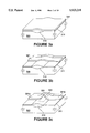
- FIG. 3a illustrates a perspective, partial cross-sectional view of an exemplary semiconductor wafer in accordance with the present invention
- FIG. 3b illustrates a perspective, partial cross-sectional view of the semiconductor wafer of FIG. 3a following a first patterning of a layer in accordance with the present invention
- FIG. 3c illustrates a perspective, partial cross-sectional view of the semiconductor wafer of FIG. 3b following a second patterning of the layer in accordance with the present invention
- FIG. 4 illustrates, in the form of a flow diagram, a second exemplary method for patterning a layer formed over a semiconductor substrate in accordance with the present invention
- FIG. 5a illustrates a perspective, partial cross-sectional view of an exemplary semiconductor wafer in accordance with the present invention
- FIG. 5b illustrates a perspective, partial cross-sectional view of the semiconductor wafer of FIG. 5a following a first patterning of a mask layer in accordance with the present invention
- FIG. 5c illustrates a perspective, partial cross-sectional view of the semiconductor wafer of FIG. 5b following a second patterning of the mask layer in accordance with the present invention
- FIG. 5d illustrates a perspective, partial cross-sectional view of the semiconductor wafer of FIG. 5c following an etch of an underlying layer using the patterned mask layer in accordance with the present invention
- FIG. 6 illustrates a perspective, partial cross-sectional view of another exemplary semiconductor wafer in accordance with the present invention
- FIG. 7 illustrates a perspective, partial cross-sectional view of an exemplary semiconductor wafer where the method of FIG. 4 is appropriate for patterning
- FIG. 8 illustrates, in the form of a flow diagram, a third exemplary method for patterning a layer formed over a semiconductor substrate in accordance with the present invention
- FIG. 9a illustrates a perspective, partial cross-sectional view of an exemplary semiconductor wafer in accordance with the present invention
- FIG. 9b illustrates a perspective, partial cross-sectional view of the semiconductor wafer of FIG. 9a following the patterning of a mask layer in accordance with the present invention
- FIG. 9c illustrates a perspective, partial cross-sectional view of the semiconductor wafer of FIG. 9b following an etch of an underlying layer using the patterned mask layer in accordance with the present invention
- FIG. 10a illustrates a cross-sectional view of an exemplary semiconductor wafer in accordance with the present invention
- FIG. 10b illustrates a cross-sectional view of the semiconductor wafer of FIG. 10a following an optional spacer formation in accordance with the present invention
- FIG. 10c illustrates a cross-sectional view of the semiconductor wafer of FIG. 10b following the formation of a mask layer in accordance with the present invention
- FIG. 10d illustrates a cross-sectional view of the semiconductor wafer of FIG. 10c following the patterning of the mask layer in accordance with the present invention.
- FIG. 10e illustrates a cross-sectional view of the semiconductor wafer of FIG. 10d following an etch of an underlying layer using the patterned mask layer in accordance with the present invention.
- the present invention may be used in fabricating various static random access memories (SRAM's), such as those described in the article: M. Helm, et al., "A Low Cost, Microprocessor Compatible, 18.4 ⁇ m 2 , 6-T Bulk Cell Technology for High Speed SRAMs," 1993 Symposium on VLSI Technology: Digest of Technical Papers, 1993 VLSI Technology Symposium, Kyoto, May 17-19, 1993, pp. 65-66. That article is herein incorporated by reference. However, it is to be understood that the present invention is not limited to its use in SRAM fabrication technology but rather, for example, may also be used in fabricating various other types of semiconductor devices.
- SRAM's static random access memories
- a semiconductor substrate is provided as illustrated in FIG. 3a by substrate 300, in FIG. 5a by substrate 500, in FIG. 6 by substrate 600, in FIG. 7 by substrate 700, in FIG. 9a by substrate 900, and in FIG. 10a by substrate 1000.
- This substrate may be a silicon substrate, yet it is to be appreciated that a variety of other types of semiconductor substrates may be used, for example, depending upon one's specific design and/or functional requirements for the semiconductor device to be fabricated.
- the views of FIGS. 3a-3c, 5a-5d, 6, 7, 9a-9c, and 10a-10e are merely partial views of a larger semiconductor wafer so as to provide for a clearer understanding of the present invention.
- the present invention may also be used in patterning layers elsewhere on the substrate partially illustrated in the drawings.
- FIG. 2 illustrates, in the form of a flow diagram, a first exemplary method for patterning a layer formed over a semiconductor substrate in accordance with the present invention. So as to better explain this first exemplary method of the present invention, FIGS. 3a, 3b, and 3c will be used to illustrate the steps performed in the method of FIG. 2.
- a field oxide region is formed over the semiconductor substrate, as illustrated in FIG. 3a where field oxide region 310 has been formed over substrate 300.
- This field oxide region may be formed using any suitable process, for example a LOCal Oxidation of Silicon (LOCOS) isolation process, and may serve to isolate separate active regions on the substrate from one another. While the field oxide region is illustrated in FIG. 3a as being raised above the surface of the substrate with a bird's beak form, it is to be understood that the field oxide region may be formed differently as the form of the field oxide region may depend on the process used to form this region.
- the field oxide region may, for example, be level with the surface of the substrate.
- a gate oxide layer may then be formed over the active regions of the substrate in step 205 of FIG.
- gate oxide layer 311 has been formed over substrate 300.
- This gate oxide layer contains silicon dioxide (SiO 2 ) and may be grown on or deposited over the surface of the wafer.
- the gate oxide layer may be approximately 100 Angstroms ( ⁇ ) to approximately 150 ⁇ in thickness. Other thicknesses may also be used, however.
- Approximately 1500 ⁇ to approximately 3000 ⁇ of polysilicon may then be deposited over the wafer in step 210 of FIG. 2, as illustrated in FIG. 3a where polysilicon layer 320 has been deposited over substrate 300. Other thicknesses of polysilicon may also be used here.
- the polysilicon may now be patterned in step 215 of FIG. 2 to form polysilicon gates over the wafer.
- the polysilicon layer may be patterned into a polysilicon line pattern which crosses over two active regions separated by the field oxide region, as illustrated in FIG. 3b where polysilicon layer 320 of FIG. 3a has been etched to form polysilicon line pattern 321 which crosses over two active regions separated by field oxide region 310.
- any suitable patterning process may be used.
- a layer of photosensitive material such as photoresist may be formed over the wafer, exposed to radiation such as ultraviolet radiation through a suitable line pattern mask, and developed to define in the photosensitive material the polysilicon line pattern to be etched from the underlying polysilicon layer.
- the polysilicon layer may then be etched using a suitable etch technique and chemistry to form the polysilicon line pattern.
- a suitable etch technique and chemistry may be used.
- the etch may be selective to oxide to protect against spiking through the gate oxide layer.
- the remaining photosensitive material may then be removed following the polysilicon etch.
- the polysilicon line pattern may be patterned into appropriate polysilicon gates. This is illustrated in FIG. 3c where polysilicon line pattern 321 of FIG. 3b has been patterned into polysilicon gates 321a and 321b by etching a gap 322 in polysilicon line pattern 321.
- any suitable patterning process may be used.
- a layer of photosensitive material such as photoresist may be formed over the wafer, exposed to radiation such as ultraviolet radiation through a suitable gap mask, and developed to define in the photosensitive material the gap to be etched from the polysilicon line pattern.
- the shape of the gap pattern in the photosensitive material is illustrated in FIG. 3c by dashed-line rectangle 323.
- the gap pattern is not limited to this illustrated shape but rather may be shaped differently in defining the gap to be etched from the polysilicon line pattern.
- the gap pattern may be shaped so as to extend across more than one polysilicon line pattern so that polysilicon gates may be formed elsewhere over the wafer.
- the gap pattern in the photosensitive material preferably exposes the entire width of the polysilicon line pattern so as to ensure the polysilicon line pattern will be completely separated by the gap to be etched. It is to be appreciated that the gap pattern in the photosensitive material may expose portions of the field oxide region which are not covered by the polysilicon line pattern. The gap may then be etched from the polysilicon line pattern using a suitable etch technique and chemistry.
- a polysilicon:oxide selective etch is used as portions of the field oxide region which are not covered by the polysilicon line pattern and which are exposed by the gap pattern in the photosensitive material may be subjected to this etch.
- the selectivity of this etch may be approximately 25:1, yet other suitable polysilicon:oxide selectivity ratios may also be used.
- the selectivity ratio for this etch may depend, for example, on the thicknesses of the polysilicon layer and the underlying oxide layer.
- the gap etch essentially serves to "cut" the polysilicon line pattern as the features of the gap pattern are perpendicular or substantially perpendicular to the polysilicon line pattern. Accordingly, the lithographic rounding effects replicated at the ends of each polysilicon gate as a result of typical lithography processes are avoided. In applying the endcap rule, then, lithographic rounding effects need not be considered in determining the amount each polysilicon gate should extend over the edge of its active region. Transistors may thus be placed closer to one another over the wafer, providing for the fabrication of semiconductor devices with higher packing densities. Referring to the example given above, each polysilicon gate need only extend over the edge of its active region for approximately 0.25 ⁇ m.
- the endcap rule need only account for line width variation and misalignment; the approximately 0.15 ⁇ m extension to account for lithographic rounding effects is no longer needed.
- the spacing between transistors may be only approximately 1.0 ⁇ m (0.25 ⁇ m first polysilicon gate extension +0.5 ⁇ m polypoly spacing +0.25 ⁇ m second polysilicon gate extension), as compared to the 1.4 ⁇ m spacing required above where the compensation for lithographic rounding effects increased this spacing.
- the gap pattern may be etched from the polysilicon layer prior to the etching of the polysilicon line pattern from the polysilicon layer.
- the gap pattern and polysilicon line pattern may be etched using suitable etch techniques and chemistries.
- the polysilicon line pattern etch here, may be a polysilicon:oxide selective etch as portions of the field oxide region may be subjected to this line pattern etch as a result of becoming exposed because of the gap etch.
- FIG. 4 illustrates, in the form of a flow diagram, a second exemplary method for patterning a layer formed over a semiconductor substrate in accordance with the present invention. So as to better explain this second exemplary method of the present invention, FIGS. 5a, 5b, 5c, and 5d will be used to illustrate the steps performed in the method of FIG. 4.
- Steps 400, 405, and 410 of FIG. 4 are similarly performed as steps 200, 205, and 210 of FIG. 2, respectively, discussed above.
- the above discussion pertaining to steps 200, 205, and 210 therefore similarly applies here as well.
- a field oxide region, gate oxide layer, and polysilicon layer are formed over a semiconductor substrate. This is illustrated in FIG. 5a where field oxide region 510, gate oxide layer 511, and polysilicon layer 520 have been formed over substrate 500.
- a mask layer is formed over the wafer, as illustrated in FIG. 5a where mask layer 530 has been formed over substrate 500.
- the mask layer may contain any suitable material or materials which may be patterned to provide for a mask when the underlying polysilicon layer is etched.
- the mask layer may be a hard mask layer, for example.
- the mask layer may comprise approximately 200 ⁇ to approximately 2000 ⁇ of silicon dioxide (SiO 2 ) or of silicon nitride (Si 3 N 4 ), for example. Other thicknesses of these materials may also be used and may depend, for example, on the deposition technique used to form this mask layer or the etch technique used to etch this mask layer.
- the mask layer comprises silicon dioxide (SiO 2 )
- it may be deposited or grown over the polysilicon layer.
- the mask layer is then patterned in step 420 of FIG. 4 to define the pattern for polysilicon gates to be etched from the underlying polysilicon layer.
- the mask layer may first be patterned to define a line pattern for the underlying polysilicon layer. This line pattern in the mask crosses over two active regions separated by the field oxide region, as illustrated in FIG. 5b where mask layer 530 of FIG. 5a has been patterned to form line pattern 531 which crosses over two active regions separated by field oxide region 510.
- any suitable patterning process may be used.
- a layer of photosensitive material such as photoresist may be formed over the wafer, exposed to radiation such as ultraviolet radiation through a suitable line pattern mask, and developed to define in the photosensitive material the line pattern to be etched from the mask layer.
- the mask layer may then be etched using a suitable etch technique and chemistry to form the line pattern.
- a timed etch or an endpoint etch may be used.
- the etch may be selective to polysilicon to protect the underlying polysilicon layer from any overetch. It is to be appreciated, though, that the etch technique used here does not have to be highly selective to polysilicon because the underlying polysilicon which may be subjected to any overetch will later be removed. The remaining photosensitive material may then be removed following this etch.
- the line pattern may be patterned again to define the polysilicon gates to be etched from the underlying polysilicon layer. That is, a gap may be formed in the line pattern, as illustrated in FIG. 5c where line pattern 531 of FIG. 5b has been patterned into gate patterns 531a and 531b by forming a gap 532 in line pattern 531.
- any suitable patterning process may be used.
- the mask is a hard mask, for example, a layer of photosensitive material such as photoresist may be formed over the wafer; exposed to radiation such as ultraviolet radiation through a suitable gap mask, and developed to define in the photosensitive material the gap to be etched from the mask line pattern.
- the shape of the gap pattern in the photosensitive material is illustrated in FIG. 5c by dashed-line rectangle 533. It is to be understood, however, that the gap pattern is not limited to this illustrated shape but rather may be shaped differently in defining the gap to be etched from the mask line pattern. For example, the gap pattern may be shaped so as to extend across more than one mask line pattern so that polysilicon gates may be formed elsewhere over the wafer using this same mask.
- the gap pattern in the photosensitive material preferably exposes the entire width of the line pattern so as to ensure that the line pattern will be completely separated by the gap to be etched. It is to be appreciated that the gap pattern in the photosensitive material may expose portions of the polysilicon layer which are not covered by the mask line pattern.
- the gap may then be etched from the mask line pattern using a suitable etch technique and chemistry.
- a suitable etch technique and chemistry For example, a timed or endpoint etch may be used.
- the etch may be selective to polysilicon to protect portions of the polysilicon layer which are not covered by the mask line pattern and which are exposed by the gap pattern in the photosensitive material.
- the mask layer comprises oxide
- the oxide:polysilicon selectivity of this etch may be in the range of approximately 5:1 to approximately 10:1.
- Other suitable selectivity ratios may also be used, however, and may depend on the thicknesses of the mask layer and the underlying polysilicon layer.
- the underlying polysilicon layer may now be etched in step 425 of FIG. 4 using the pattern created in the mask layer as a mask to form the polysilicon gates. That is, the polysilicon layer is etched to replicate in the polysilicon layer the pattern of the mask. This is illustrated in FIG. 5d where polysilicon layer 520 of FIGS. 5a-5c has been etched using gate patterns 531a and 531b as a mask to form polysilicon gates 521a and 521b.
- any suitable etch technique and chemistry may be used.
- a polysilicon:oxide selective etch may be used where the mask layer comprises silicon dioxide (SiO 2 ).
- This selective etch would also protect against spiking through the gate oxide layer.
- an etch selective to nitride may be used where the mask layer comprises silicon nitride (Si 3 N 4 ). This etch may be a timed etch or an endpoint etch to minimize any overetch of the underlying gate oxide layer.
- the remaining mask 531a and 531b is then removed from the wafer in step 430 of FIG. 4.
- the gap formation essentially serves to "cut" the mask line pattern as the features of the gap pattern are perpendicular or substantially perpendicular to the mask line pattern. Accordingly, the lithographic rounding effects replicated at the ends of each polysilicon gate as a result of typical lithography processes are avoided. In applying the endcap rule then, as discussed above with regard to the method of FIG. 2, lithographic rounding effects need not be considered in determining the amount each polysilicon gate should extend over the edge of its active region. Transistors may thus be placed closer to one another over the wafer, providing for the fabrication of semiconductor devices with higher packing densities.
- the gap pattern may be formed from the mask layer prior to the formation of the mask line pattern from the mask layer.
- the gap pattern and the mask line pattern may be etched using suitable etch techniques and chemistries.
- the mask line pattern etch here, may be selective to polysilicon as portions of the underlying polysilicon layer may be subjected to this line pattern etch as a result of becoming exposed because of the gap etch.
- a photosensitive material may be used for the mask to pattern the underlying polysilicon layer.
- a photosensitive material such as photoresist may be formed over the polysilicon layer.
- the photosensitive material may then be exposed to radiation such as ultraviolet radiation through separate masks having features perpendicular or substantially perpendicular to one another.
- a positive photoresist may be exposed to radiation such as ultraviolet radiation through a suitable line pattern mask and through a separate, suitable gap mask. This is illustrated in FIG. 6 where photoresist layer 630 has been exposed to radiation through a line pattern mask and through a separate gap mask.
- Photoresist layer 630 here has been formed over polysilicon layer 620, which has been formed over substrate 600 having field oxide region 610 and gate oxide layer 611. As illustrated in FIG. 6, photoresist layer 630 has been exposed to radiation through a line pattern mask in shaded regions 631 and 632. Photoresist layer 630 has also been exposed to radiation through a gap mask in shaded region 633. These separate masks may be used in any order. It is to be appreciated that portions of shaded regions 631 and 633 overlap and that portions of shaded regions 632 and 633 likewise overlap. The exposed portions of the positive photoresist will dissolve in the developer, leaving gate patterns similar to gate patterns 531a and 531b illustrated in FIG. 5c over the polysilicon layer.
- the underlying polysilicon layer may then be patterned using a suitable etch technique and chemistry.
- a timed etch or an endpoint etch may be used.
- the etch may be selective to oxide to protect against spiking through the gate oxide layer.
- the remaining photosensitive material may then be removed following the polysilicon etch, leaving polysilicon gates similar to polysilicon gates 521a and 521b illustrated in FIG. 5d.
- FIG. 4 may be more appropriate for patterning the polysilicon layer into polysilicon gates where two neighboring transistors are to share a common active region, as illustrated in FIG. 7 where polysilicon gates 721a and 721b share common active region 770. If the method of FIG. 2 were used, a portion of the common active region which is illustrated in FIG. 7 as shaded portion 771 may be subjected to a double overetch from two etch processes: one for the polysilicon line pattern and one for the gap pattern. As this common active region may be covered with only a thin gate oxide layer as illustrated in FIG.
- the double overetch of the polysilicon layer may spike through the gate oxide layer and etch into the underlying substrate.
- the line and gap patterning are both simultaneously transferred to the polysilicon layer through the mask layer.
- the polysilicon layer is then etched only once, thus avoiding the possible spiking of the gate oxide layer due to a double overetch.
- the present invention may also be used in conjunction with other processing techniques.
- the present invention may be used to pattern layers in fabricating semiconductor devices where selectively silicided polysilicon is used.
- the present invention may also be used with self-aligned contact processes.
- FIG. 8 illustrates, in the form of a flow diagram, a third exemplary method in accordance with the present invention for patterning a layer formed over a semiconductor substrate in conjunction with such other processing techniques. So as to better explain this third exemplary method of the present invention, FIGS. 9a, 9b, and 9c will be used to illustrate the steps performed in the method of FIG. 8.
- Steps 800, 805, and 810 of FIG. 8 are similarly performed as steps 200, 205, and 210 of FIG. 2, respectively, discussed above.
- the above discussion pertaining to steps 200, 205, and 210 therefore similarly applies here as well.
- a field oxide region, a gate oxide layer, and a polysilicon layer are formed over a semiconductor substrate. This is illustrated in FIG. 9a where field oxide regions 910, gate oxide layer 911, and polysilicon layer 920 have been formed over substrate 900.
- a first mask layer is then formed over the wafer in step 815 of FIG. 8.
- the material used for the first mask layer may be, for example, silicon dioxide (SiO 2 ), silicon nitride (Si 3 N 4 ), or some other hard mask material. Another suitable material or materials may also be used. While a first mask layer comprising silicon dioxide (SiO 2 ) may be grown over the wafer, it is preferably deposited as the growth of this layer may unduly deplete the underlying polysilicon layer of silicon. Where the first mask layer is a hard mask layer, the thickness of this first mask layer may be, for example, approximately 2000 ⁇ to approximately 3000 ⁇ . Other thicknesses may also be used, though, and may depend on the material used for the first mask layer.
- the thickness of the first mask layer may also depend on other processing considerations, such as subsequent etch techniques and chemistries used to etch polysilicon gates from the underlying polysilicon layer. As this first mask layer may serve to insulate self-aligned contacts from the polysilicon gates, the material or materials used for the first mask layer are preferably dielectric. A first mask comprising a dielectric material will also prevent any silicide formation over underlying portions of the polysilicon gates. This is discussed in more detail below.
- This first mask layer may then be patterned in step 820 of FIG. 8, as illustrated in FIG. 9a where patterned first mask layer 940 has been formed over polysilicon layer 920.
- the patterned first mask may serve to define where self-aligned contacts will be formed if the first mask is to be used to insulate self-aligned contacts from the polysilicon gates.
- the patterned first mask may also define the polysilicon areas which are to be silicided as the patterned first mask may prevent or block underlying polysilicon from reacting with a later deposited material in forming a silicide layer over select portions of the polysilicon. In patterning the first mask layer here, any suitable patterning process may be used.
- the first mask layer is a hard mask layer
- a layer of photosensitive material such as photoresist may be formed over the wafer, exposed to radiation such as ultraviolet radiation through a suitable silicide-block mask, and developed to define in the photosensitive material the silicide-block pattern to be etched from the first mask layer.
- the term "silicide-block” is not meant to be used in a limiting sense but rather is merely used as a convenient label. That is, the use of the term “silicide-block” is not to be construed as a requirement that the first mask be used to block silicide formation from portions of the underlying layer.
- the silicide-block pattern may then be etched from the first mask layer using a suitable etch technique and chemistry. For example, a timed etch or an endpoint etch may be used. The etch may be selective to polysilicon to minimize any overetch effects on the underlying polysilicon. As portions of this polysilicon will remain as part of the polysilicon gates formed over the wafer, the polysilicon is preferably subjected to as little overetch as possible. The remaining photosensitive material may then be removed following this etch.
- a suitable etch technique and chemistry For example, a timed etch or an endpoint etch may be used. The etch may be selective to polysilicon to minimize any overetch effects on the underlying polysilicon. As portions of this polysilicon will remain as part of the polysilicon gates formed over the wafer, the polysilicon is preferably subjected to as little overetch as possible. The remaining photosensitive material may then be removed following this etch.
- steps 825, 830, 835, and 840 of FIG. 8 may then be performed to pattern the polysilicon layer. It is to be appreciated that the first mask layer may also be patterned in the performance of these steps. Steps 825, 830, 835, and 840 of FIG. 8 correspond to steps 415, 420, 425, and 430 of FIG. 4 discussed above. Accordingly, the above discussion pertaining to steps 415, 420, 425, and 430, including the discussion pertaining to the use of photosensitive material for the mask of FIG. 4, similarly applies here as well.
- a second mask layer is formed over the semiconductor wafer in step 825 of FIG. 8.
- the second mask layer may contain any suitable material or materials which may be patterned to provide for a mask when the underlying polysilicon layer is etched.
- the second mask layer may be a hard mask layer, for example, comprising silicon dioxide (SiO 2 ), which may be deposited or grown over the polysilicon layer, or comprising silicon nitride (Si 3 N 4 ).
- the second mask layer may be of any suitable thickness. This thickness may depend, for example, on the deposition technique used to form this mask layer or any etch technique used to etch this mask layer. Where the second mask layer is a hard mask layer and where the first mask layer is to be etched while patterning the second mask layer, the thickness of the second mask layer is preferably no more than approximately 20 percent of the thickness of the first mask layer.
- the second mask layer is then patterned in step 830 of FIG. 8 to define the pattern for polysilicon gates to be etched from the underlying polysilicon layer, as illustrated in FIG. 9b where the second mask layer has been patterned into gate patterns 951a, 951b, 951c, 951d, 951e, and 951f.
- the second mask layer may first be patterned to define a line pattern for the underlying polysilicon layer. This line pattern in the second mask crosses over active regions separated by field oxide regions. In patterning the second mask layer here, any suitable patterning process may be used.
- the second mask layer is a hard mask layer
- a layer of photosensitive material such as photoresist may be formed over the wafer, exposed to radiation such as ultraviolet radiation through a suitable line pattern mask, and developed to define in the photosensitive material the line pattern to be etched from the second mask layer.
- the second mask layer may then be etched using a suitable etch technique and chemistry to form the line pattern.
- the remaining photosensitive material may then be removed following this etch.
- portions of the first mask layer which underlie the second mask layer may also be etched in patterning the second mask layer, as illustrated in FIG. 9b where the first mask of FIG. 9a has been patterned into silicide-block patterns 941a and 941b.
- the second mask layer may preferably comprise the same material as that of the first mask layer so as to simplify this etching process. For example, they may both comprise silicon dioxide (SiO 2 ).
- both the second mask layer and the first mask layer may then be etched in one process step. For example, an etch selective to polysilicon may be used here so as to ensure that both the first and second mask layers are fully etched without etching through the underlying polysilicon, and thus through the gate oxide layer into the underlying substrate.
- the line pattern may be patterned again to define the polysilicon gates to be etched from the underlying polysilicon layer. That is, a gap may be formed in the line pattern of the second mask layer.
- any suitable patterning process may be used.
- the second mask is a hard mask, for example, a layer of photosensitive material such as photoresist may be formed over the wafer, exposed to radiation such as ultraviolet radiation through a suitable gap mask, and developed to define in the photosensitive material the gap to be etched from the line pattern of the second mask layer.
- the gap pattern in the photosensitive material preferably exposes the entire width of the line pattern so as to ensure that the line pattern will be completely separated by the gap to be etched.
- the gap pattern in the photosensitive material may expose portions of the polysilicon layer which are not covered by the line pattern of the second mask layer.
- the gap may then be etched from the mask line pattern using a suitable etch technique and chemistry.
- the pattern to create polysilicon gates from the underlying polysilicon layer remains, as illustrated in FIG. 9b.
- the gap pattern may be formed from the second mask layer prior to the formation of the line pattern from the second mask layer.
- the second mask layer is a hard mask layer
- the gap pattern and the mask line pattern may be etched using suitable etch techniques and chemistries.
- the mask line pattern etch here, may be selective to polysilicon as portions of the underlying polysilicon may be subjected to this line pattern etch as a result of becoming exposed because of the gap etch.
- the photosensitive material may be exposed to radiation such as ultraviolet radiation through a suitable line pattern mask and through a separate, suitable gap mask. These separate masks may be used in any order.
- the exposed portions of positive photoresist may then be dissolved in developer leaving suitable gate patterns over the polysilicon layer, as illustrated in FIG. 9b where the second mask layer has been patterned into gate patterns 951a, 951b, 951c, 951d, 951e, and 951f.
- As portions of the first mask layer may remain exposed over the surface of the wafer, these portions may then be etched using a suitable etch technique and chemistry to create silicide-block patterns, as illustrated in FIG. 9b where the first mask of FIG. 9a has been patterned into silicide-block patterns 941a and 941b.
- the underlying polysilicon layer may now be etched in step 835 of FIG. 8 using the pattern created in the second mask layer as a mask to form the polysilicon gates. That is, the polysilicon layer is etched to replicate in the polysilicon layer the pattern of the second mask. This is illustrated in FIG. 9c where polysilicon layer 920 of FIGS. 9a-9b has been etched using gate patterns 951a, 951b, 951c, 951d, 951e, and 951f as a mask to form polysilicon gates 921a, 921b, 921c, 921d, 921e, and 921f, respectively. In etching the polysilicon layer using the second mask, any suitable etch technique and chemistry may be used. The remaining second mask is then removed from the wafer in step 840 of FIG. 8.
- the gap formation essentially serves to "cut" the line pattern in the second mask layer as the features of the gap pattern are perpendicular or substantially perpendicular to this line pattern. Accordingly, lithographic rounding effects replicated at the ends of each polysilicon gate as a result of typical lithography processes are avoided. In applying the endcap rule then, as discussed above with regard to the method of FIG. 2, lithographic rounding effects need not be considered in determining the amount each polysilicon gate should extend over the edge of its active region. Transistors may thus be placed closer to one another over the wafer, providing for the fabrication of semiconductor devices with higher packing densities.
- the semiconductor wafer may be selectively silicided in step 845 of FIG. 8.
- suitable sidewall spacers may be formed to cover the sides of the polysilicon gates.
- these sidewall spacers are made of a dielectric material, such as silicon dioxide (SiO 2 ) or silicon nitride (Si 3 N 4 ), as these sidewall spacers may serve to prevent silicide formation on the covered portions, thus ensuring no shorts are created between the polysilicon gates and any diffusion regions in the substrate as a result of this silicide process.
- the gate oxide layer may also be etched prior to this selective silicide process so as to define diffusion regions in the substrate which may also be silicided.
- a metal layer may then be deposited over the wafer. While in one embodiment this metal comprises titanium (Ti), other suitable materials such as cobalt (Co) may also be used here. As a general example, any refractory metal which can withstand subsequent processing temperatures may be used. When the wafer is heated, then, the metal layer will react with silicon in the polysilicon gates and in other areas containing silicon which are in direct contact with the metal, such as any diffusion regions in the substrate. Such a reaction produces a silicide layer. For example, a layer of titanium silicide (TiSi 2 ) or of cobalt silicide (CoSi 2 ) is formed where the metal layer contains titanium (Ti) or cobalt (Co), respectively.
- TiSi 2 titanium silicide
- CoSi 2 cobalt silicide
- the resulting silicide layer may, for example, serve to reduce the resistivity of the silicided regions. For example, the resistivity of those portions of the polysilicon gates which have been silicided may be reduced as a result of this silicide process.
- the metal layer does not react with silicon dioxide (SiO 2 ), for example the field oxide regions, or with regions not containing silicon. It is to be appreciated that where the first mask comprises a dielectric material such as SiO 2 , the metal will not react with those portions of the polysilicon gates covered by the silicide-block patterns in the first mask, as illustrated in FIG.
- silicide-block patterns 941a and 941b respectively, from first mask layer 940 of FIG. 9a. Any unreacted metal may then be removed from the substrate following this silicide process, for example by using an etchant which does not attack the silicide, the substrate, or silicon dioxide. While the diffusion regions may be implanted after this silicide process, it is to be understood that the diffusion regions may be implanted at other times, for example just prior to this silicide process. Furthermore, the above silicide process may be more appropriately termed a salicide process--that is, a Self-ALigned sillCIDE process--as the silicide regions may be formed without concern for the alignment of any masks or patterns.
- silicide processes may be used to form various silicide layers over the polysilicon gates and/or any diffusion regions.
- a silicide layer may be deposited over the wafer and selectively etched to define silicide layers over the polysilicon gates and/or diffusion regions.
- tungsten silicide WSi 2
- the polysilicon gates and/or any diffusion regions are described above as being silicided after the second mask has been removed, the polysilicon gates and/or any diffusion regions may be silicided at other times as well.
- the polysilicon layer formed over the wafer in step 810 of FIG. 8 may be silicided prior to the formation of the first mask layer in step 815 of FIG. 8. Where this is done, however, the etch technique and chemistry used to etch polysilicon gates from the polysilicon layer may need to account for the silicide layer over the polysilicon.
- self-aligned contacts may be formed in step 850 of FIG. 8 using suitable process steps as required for the desired semiconductor device being fabricated. It is to be appreciated that a self-aligned contact may be formed, for example, between polysilicon gates, as illustrated in FIG. 9c where a self-aligned contact may be formed in gap 960 between polysilicon gates 921a and 921b. The self-aligned contact may be formed to provide for an electrical connection to the underlying substrate, for example to a diffusion region in the substrate. The material from the first mask layer which remains over the polysilicon gates, as illustrated in FIG.
- silicide-block patterns 941a and 941b may be used in forming this self-aligned contact as the self-aligned contact must be insulated from the polysilicon gates to avoid shorting the gates to the underlying substrate through the self-aligned contact.
- sidewall spacers may also be used to insulate the self-aligned contact from the polysilicon gates.
- silicide process and the self-aligned contact process are not necessary in practicing the present invention. More clearly, the silicide process and the self-aligned contact process are optional processes; neither process, either process, or both processes may be used in practicing the present invention to create transistor gates.
- FIGS. 10a, 10b, 10c, 10d, and 10e illustrate, in cross-sectional views of a semiconductor wafer, another exemplary application of the method of FIG. 8.
- steps 800, 805, and 810 are similarly performed as described above, and thus the above discussion pertaining to these steps applies here as well.
- FIG. 10a illustrates in cross-sectional views of a semiconductor wafer, another exemplary application of the method of FIG. 8.
- steps 800, 805, and 810 are similarly performed as described above, and thus the above discussion pertaining to these steps applies here as well.
- FIG. 10a where field oxide regions 1010, gate oxide layer 1011, and polysilicon layer 1020 have been formed over substrate 1000.
- Steps 815 and 820 of FIG. 8 are also similarly performed as described above, and thus the above discussion pertaining these steps applies here as well.
- the first mask layer here may be patterned not only as described above but also to define a gap to be etched from the underlying polysilicon layer.
- the patterned first mask is illustrated in FIG. 10a where the first mask layer has been patterned into regions 1040a and 1040b and has been patterned to define gap 1070.
- the silicide-block pattern and the gap pattern may be either simultaneously etched from the first mask layer or separately etched using a suitable etch technique and chemistry. When separately etched, the silicide-block pattern and the gap pattern may be etched from the first mask layer in any order.
- spacers may be added to the gap region of the patterned first mask, as illustrated in FIG. 10b where sidewall spacers 1071a and 1071b have been formed in gap 1070.
- These spacers may comprise any suitable material.
- silicon dioxide (SiO 2 ) or silicon nitride (Si 3 N 4 ) may be used.
- the spacers may comprise a material that is the same or different from that used for the first mask layer.
- any suitable processing technique may be used. For example, a layer of the material used for the spacers may be deposited over the semiconductor wafer.
- a suitable anisotropic etch may then be used to remove portions of the deposited layer, leaving spacers in the gap defined in the first mask. Sidewall spacers may also be left on other portions of the wafer, as illustrated in FIG. 10b where sidewall spacers 1081a and 1081b have also been formed on the sides of patterned regions 1040a and 1040b, respectively.
- this spacer formation is optional; it is not necessary to implement the spacer technique to practice the method of FIG. 8 for this exemplary application. With or without this spacer formation, steps 825 through 850 are nevertheless performed in substantially the same manner as summarized below. That is, implementing the optional spacer formation does not substantially alter the exemplary application of the method of FIG. 8 here. Furthermore, the use of spacers advantageously reduces the width of the gap formed in the first mask. When this gap has been defined as small as lithographic resolution permits, then, the spacing between two polysilicon gates as defined by this gap may be made smaller than lithographically possible because of the spacer formation. This is discussed in further detail below.
- FIG. 10c illustrates the formation of a second mask layer in step 825 of FIG. 8 where second mask layer 1050 has been formed over the semiconductor wafer.
- the second mask layer may be first patterned to define the gap between polysilicon gates, as illustrated in FIG. 10d where a portion of the second mask layer 1050 has been removed from gap 1070.
- the gap defined in the second mask layer may be wider than the gap defined in the first mask layer. This allows for some misalignment of the gap mask in patterning the gap in the second mask layer so that it overlies the gap patterned in the first mask layer.
- the error margin for this alignment should not be so large that a potential gap in the second mask layer would directly overlie any polysilicon not covered by the gap region and the silicide-block pattern regions in the first mask layer.
- any suitable etch technique and chemistry may be used to etch the gap from the second mask layer.
- the etch technique may depend on the specific materials used for the first mask, the second mask, and any sidewall spacers in the gap defined by the first mask.
- the etch technique may also depend on whether a second mask comprising silicon dioxide (SiO 2 ) was grown or deposited over the wafer.
- a timed etch may be used where the second mask layer has been deposited over the wafer, regardless of the materials used for the first mask, the second mask, or any sidewall spacers.
- a selective etch may be used where the material used for the first mask is different from material deposited for the second mask layer.
- the selective etch would avoid gouging into the first mask while etching the gap in the second mask.
- the etch technique is preferably also selective to the material used for any sidewall spacers in the first mask gap to prevent them from being etched.
- the etch technique used may be anisotropic to protect any sidewall spacers in the gap defined by the first mask from being etched.
- spacers from the second mask may be formed covering any original sidewall spacers in the first mask gap as a result of such an anisotropic etch.
- the second mask layer is also patterned to define the line pattern for the underlying polysilicon layer as described above.
- the second mask layer is a hard mask layer and is etched to form the line pattern
- portions of the first mask layer which underlie the second mask layer may also be etched in forming the line pattern.
- FIG. 10d where the first mask regions 1040a and 1040b of FIG. 10a have been patterned into silicide-block patterns 1041a and 1041b.
- the second mask layer is patterned into gate patterns to define, possibly in conjunction with the silicide-block patterns of the first mask layer, the polysilicon gates to be etched from the underlying polysilicon layer. This is illustrated in FIG. 10d where gate patterns 1051a and 1051b and silicide-block patterns 1041a and 1041b remain over the surface of the wafer.
- FIG. 10e illustrates the formation of polysilicon gates 1021a and 1021b which have been etched from polysilicon layer 1020 using gate patterns 1051a and 1051b.
- the etch technique and chemistry used to etch the polysilicon layer may depend on the materials used for the first mask, the second mask, and any sidewall spacers in-the gap of the first mask.
- the spacing between polysilicon gates may be made smaller than lithographically possible as the gate patterns are replicated in the underlying polysilicon layer. Accordingly, the spacing between transistors may be reduced because of this reduced poly-poly spacing.
- Steps 845 and 850 of FIG. 8 may now be similarly performed as described above.
- the patterning of the gap pattern in the first mask layer as described in the above exemplary application of the method of FIG. 8 as illustrated in FIGS. 10a-10e is preferably performed to allow for a less critical alignment of the gap mask in patterning the gap in the second mask layer. With higher tolerances for inaccuracies in aligning this gap mask, then, less expensive equipment may be used than would otherwise be needed if the gap were not initially formed in the first mask layer as discussed above. If the gap were not initially formed in the first mask layer, for example, it may be formed from the first mask layer in accordance with the gap formed in the second mask. Where the first and second mask layers are hard mask layers, for example, the gaps in the first mask and the second mask may be etched simultaneously or separately.
- the materials used for the first and second mask are preferably the same so as to simplify this etch process.
- the alignment of the gap mask in patterning the gap in the second mask layer is more critical as the gap in the second mask layer will be used to define the spacing between two polysilicon gates. More costly equipment would then be needed to provide for such a critical alignment.
- the resulting semiconductor wafer may now be used in fabricating various semiconductor devices and integrated circuits including, but not limited to, those for various semiconductor memory components such as SRAMs, microprocessors, and various other semiconductor devices.
- sidewall spacers of a suitable material may also be formed in the gap defined by the second mask used in the method of FIG. 8 to obtain sub-lithographic spacings between transistor gates.
- Sidewall spacers of a suitable material may also be formed in the gap defined by the mask used in the method of FIG. 4 for this same purpose.
- the thicknesses of these masks may need to be increased to accommodate such sidewall spacers.
- a phase-shift mask may also be used to provide for sublithographic spacings.
- a method for avoiding lithographic rounding effects for semiconductor fabrication has thus been described.
- a patterning or etch process which reduces or avoids lithographic rounding effects may now be used in fabricating various semiconductor devices.
- the present invention may also be used to reduce the minimum extension of a transistor gate over the edge of its active region under the endcap rule.
- the present invention may be used for fabricating semiconductor devices with higher packing densities as transistors may be placed closer to one another in fabricating semiconductor devices.
- the present invention may also be used in patterning or etching layers for purposes other than those with regard to the formation of transistor gates.
- the present invention is not meant to be limited to only the specific purpose of patterning transistor gates but rather may also be used in patterning or etching any layer or layers in fabricating various semiconductor devices.
- the present invention may be used in lieu of typical lithography processes so as to reduce or avoid lithographic rounding effects in patterning a given layer of material.
- the present invention may thus be used in this example merely to obtain more well-defined patterns for semiconductor fabrication.
- separate masks having features perpendicular or substantially perpendicular to one another may be used in a manner similar to that described above to provide for such well-defined patterns.
Abstract
Description
Claims (30)
Priority Applications (1)
| Application Number | Priority Date | Filing Date | Title |
|---|---|---|---|
| US08/235,509 US5523258A (en) | 1994-04-29 | 1994-04-29 | Method for avoiding lithographic rounding effects for semiconductor fabrication |
Applications Claiming Priority (1)
| Application Number | Priority Date | Filing Date | Title |
|---|---|---|---|
| US08/235,509 US5523258A (en) | 1994-04-29 | 1994-04-29 | Method for avoiding lithographic rounding effects for semiconductor fabrication |
Publications (1)
| Publication Number | Publication Date |
|---|---|
| US5523258A true US5523258A (en) | 1996-06-04 |
Family
ID=22885803
Family Applications (1)
| Application Number | Title | Priority Date | Filing Date |
|---|---|---|---|
| US08/235,509 Expired - Lifetime US5523258A (en) | 1994-04-29 | 1994-04-29 | Method for avoiding lithographic rounding effects for semiconductor fabrication |
Country Status (1)
| Country | Link |
|---|---|
| US (1) | US5523258A (en) |
Cited By (18)
| Publication number | Priority date | Publication date | Assignee | Title |
|---|---|---|---|---|
| US5846873A (en) * | 1996-02-02 | 1998-12-08 | Micron Technology, Inc. | Method of creating ultra-small nibble structures during mosfet fabrication |
| US5877056A (en) * | 1998-01-08 | 1999-03-02 | Texas Instruments-Acer Incorporated | Ultra-short channel recessed gate MOSFET with a buried contact |
| US5888904A (en) * | 1997-08-01 | 1999-03-30 | Holtek Microelectronics Inc. | Method for manufacturing polysilicon with relatively small line width |
| WO2000004571A1 (en) * | 1998-07-15 | 2000-01-27 | Micron Technology, Inc. | Method for patterning cavities and enhanced cavity shapes for semiconductor devices |
| US6329306B1 (en) * | 1996-09-11 | 2001-12-11 | Mitsubishi Denki Kabushiki Kaisha | Fine patterning utilizing an exposure method in photolithography |
| US6362113B1 (en) * | 1999-12-30 | 2002-03-26 | Taiwan Semiconductor Manufacturing Co., Ltd. | Method of forming pattern |
| JP2002367925A (en) * | 2001-06-12 | 2002-12-20 | Mitsubishi Electric Corp | Method of manufacturing semiconductor device |
| US20040072433A1 (en) * | 2002-10-11 | 2004-04-15 | Wilson Aaron R. | Method of forming a capacitor |
| US6756315B1 (en) | 2000-09-29 | 2004-06-29 | Cypress Semiconductor Corporation | Method of forming contact openings |
| US6803318B1 (en) | 2000-09-14 | 2004-10-12 | Cypress Semiconductor Corp. | Method of forming self aligned contacts |
| US20050100799A1 (en) * | 2003-11-06 | 2005-05-12 | Semiconductor Leading Edge Technologies, Inc. | Photomask, and method for forming pattern |
| US20050176193A1 (en) * | 2004-01-15 | 2005-08-11 | Tae-Woong Kang | Method of forming a gate of a semiconductor device |
| US20050186802A1 (en) * | 2004-02-20 | 2005-08-25 | Busch Brett W. | Methods of Forming Openings, And Methods of Forming Container Capacitors |
| US20060024904A1 (en) * | 2003-06-24 | 2006-02-02 | Wilson Aaron R | Methods of forming a capacitors - |
| US20070105391A1 (en) * | 2001-03-29 | 2007-05-10 | Kabushiki Kaisha Toshiba | Semiconductor device fabrication method and semiconductor device |
| US7879663B2 (en) | 2007-03-08 | 2011-02-01 | Freescale Semiconductor, Inc. | Trench formation in a semiconductor material |
| US20110086512A1 (en) * | 2001-04-20 | 2011-04-14 | Kabushiki Kaisha Toshiba | Semiconductor device fabrication method and semiconductor device |
| US8399360B1 (en) | 2005-11-17 | 2013-03-19 | Cypress Semiconductor Corporation | Process for post contact-etch clean |
Citations (8)
| Publication number | Priority date | Publication date | Assignee | Title |
|---|---|---|---|---|
| US4792534A (en) * | 1985-12-25 | 1988-12-20 | Kabushiki Kaisha Toshiba | Method of manufacturing a semiconductor device involving sidewall spacer formation |
| US5023203A (en) * | 1988-07-28 | 1991-06-11 | Korea Electronics & Telecommunications Research Institute Et Al. | Method of patterning fine line width semiconductor topology using a spacer |
| US5039625A (en) * | 1990-04-27 | 1991-08-13 | Mcnc | Maximum areal density recessed oxide isolation (MADROX) process |
| JPH05105948A (en) * | 1991-10-17 | 1993-04-27 | Nippon Steel Corp | Production of steel excellent in damping characteristic |
| US5208124A (en) * | 1991-03-19 | 1993-05-04 | Hewlett-Packard Company | Method of making a mask for proximity effect correction in projection lithography |
| US5264718A (en) * | 1991-06-28 | 1993-11-23 | Texas Instruments Incorporated | EEPROM cell array with tight erase distribution |
| US5316878A (en) * | 1991-06-19 | 1994-05-31 | Oki Electric Industry Co., Ltd. | Pattern forming method and photomasks used therefor |
| US5320932A (en) * | 1990-05-09 | 1994-06-14 | Kabushiki Kaisha Toshiba | Method of forming contact holes |
-
1994
- 1994-04-29 US US08/235,509 patent/US5523258A/en not_active Expired - Lifetime
Patent Citations (8)
| Publication number | Priority date | Publication date | Assignee | Title |
|---|---|---|---|---|
| US4792534A (en) * | 1985-12-25 | 1988-12-20 | Kabushiki Kaisha Toshiba | Method of manufacturing a semiconductor device involving sidewall spacer formation |
| US5023203A (en) * | 1988-07-28 | 1991-06-11 | Korea Electronics & Telecommunications Research Institute Et Al. | Method of patterning fine line width semiconductor topology using a spacer |
| US5039625A (en) * | 1990-04-27 | 1991-08-13 | Mcnc | Maximum areal density recessed oxide isolation (MADROX) process |
| US5320932A (en) * | 1990-05-09 | 1994-06-14 | Kabushiki Kaisha Toshiba | Method of forming contact holes |
| US5208124A (en) * | 1991-03-19 | 1993-05-04 | Hewlett-Packard Company | Method of making a mask for proximity effect correction in projection lithography |
| US5316878A (en) * | 1991-06-19 | 1994-05-31 | Oki Electric Industry Co., Ltd. | Pattern forming method and photomasks used therefor |
| US5264718A (en) * | 1991-06-28 | 1993-11-23 | Texas Instruments Incorporated | EEPROM cell array with tight erase distribution |
| JPH05105948A (en) * | 1991-10-17 | 1993-04-27 | Nippon Steel Corp | Production of steel excellent in damping characteristic |
Non-Patent Citations (16)
| Title |
|---|
| "Complementary Selective Writing by Direct-Write E-Beam/Optical Lithography using Mixed Positive and Negative Resist," IBM Technical Disclosure Bulletin, vol. 33, No. 3A, pp. 62-63 (Aug. 1990). |
| "Dual-Image Resist for Single-Exposure Self-Aligned Processing," IBM Technical Disclosure Bulletin, vol. 33, No. 2, pp. 447-449 (Jul. 1990). |
| "Method to Incorporate Three Sets of Pattern Information in Two Photomasking Steps," IBM Technical Disclosure Bulletin, vol. 32, No. 8A, pp. 218-219 (Jan. 1990). |
| "Multilayer Circuit Fabrication using Double Exposure of Positive Resist," IBM Technical Disclosure Bulletin, vol. 36, No. 10, pp. 423-424 (Oct. 1993). |
| Complementary Selective Writing by Direct Write E Beam/Optical Lithography using Mixed Positive and Negative Resist, IBM Technical Disclosure Bulletin, vol. 33, No. 3A, pp. 62 63 (Aug. 1990). * |
| Dual Image Resist for Single Exposure Self Aligned Processing, IBM Technical Disclosure Bulletin, vol. 33, No. 2, pp. 447 449 (Jul. 1990). * |
| Helm, M., et al., "A Low Cost, Microprocessor Compatible, 18.4 μm2, 6-T Bulk Cell Technology for High Speed SRAMs," 1993 Symposium on VLSI Technology: Digest of Technical Papers, 1993 VLSI Technology Symposium, Kyoto, pp. 65-66 (May 17-19, 1993). |
| Helm, M., et al., A Low Cost, Microprocessor Compatible, 18.4 m 2 , 6 T Bulk Cell Technology for High Speed SRAMs, 1993 Symposium on VLSI Technology: Digest of Technical Papers, 1993 VLSI Technology Symposium, Kyoto, pp. 65 66 (May 17 19, 1993). * |
| Ikeda, S., et al., "A Polysilicon Transistor Technology for Large Capacity SRAMs," IEDM Technical Digest, International Electron Devices Meeting, San Francisco, CA, pp. 469-472 (Dec. 9-12, 1990). |
| Ikeda, S., et al., A Polysilicon Transistor Technology for Large Capacity SRAMs, IEDM Technical Digest, International Electron Devices Meeting, San Francisco, CA, pp. 469 472 (Dec. 9 12, 1990). * |
| Itabashi, K., et al., "A Split Wordline Cell for 16Mb SRAM Using Polysilicon Sidewall Contacts," IEDM Technical Digest, International Electron Devices Meeting, Washington, DC, pp. 477-480 (Dec. 8-11, 1991). |
| Itabashi, K., et al., A Split Wordline Cell for 16Mb SRAM Using Polysilicon Sidewall Contacts, IEDM Technical Digest, International Electron Devices Meeting, Washington, DC, pp. 477 480 (Dec. 8 11, 1991). * |
| Method to Incorporate Three Sets of Pattern Information in Two Photomasking Steps, IBM Technical Disclosure Bulletin, vol. 32, No. 8A, pp. 218 219 (Jan. 1990). * |
| Multilayer Circuit Fabrication using Double Exposure of Positive Resist, IBM Technical Disclosure Bulletin, vol. 36, No. 10, pp. 423 424 (Oct. 1993). * |
| Verhaar, R. D. J., et al., "A 25μm2 Bulk Full CMOS SRAM Cell Technology with Fully Overlapping Contacts," IEDM Technical Digest, International Electron Devices Meeting, San Francisco, CA, pp. 473-476 (Dec. 9-12, 1990). |
| Verhaar, R. D. J., et al., A 25 m 2 Bulk Full CMOS SRAM Cell Technology with Fully Overlapping Contacts, IEDM Technical Digest, International Electron Devices Meeting, San Francisco, CA, pp. 473 476 (Dec. 9 12, 1990). * |
Cited By (39)
| Publication number | Priority date | Publication date | Assignee | Title |
|---|---|---|---|---|
| US6180500B1 (en) * | 1996-02-02 | 2001-01-30 | Micron Technology, Inc. | Method of creating ultra-small nibble structures during MOSFET fabrication |
| US5846873A (en) * | 1996-02-02 | 1998-12-08 | Micron Technology, Inc. | Method of creating ultra-small nibble structures during mosfet fabrication |
| US6329306B1 (en) * | 1996-09-11 | 2001-12-11 | Mitsubishi Denki Kabushiki Kaisha | Fine patterning utilizing an exposure method in photolithography |
| US5888904A (en) * | 1997-08-01 | 1999-03-30 | Holtek Microelectronics Inc. | Method for manufacturing polysilicon with relatively small line width |
| US5877056A (en) * | 1998-01-08 | 1999-03-02 | Texas Instruments-Acer Incorporated | Ultra-short channel recessed gate MOSFET with a buried contact |
| EP1589573A2 (en) | 1998-07-15 | 2005-10-26 | Micron Technology, Inc. | Method for patterning cavities and enhanced cavity shapes for semiconductor devices |
| WO2000004571A1 (en) * | 1998-07-15 | 2000-01-27 | Micron Technology, Inc. | Method for patterning cavities and enhanced cavity shapes for semiconductor devices |
| US6190989B1 (en) * | 1998-07-15 | 2001-02-20 | Micron Technology, Inc. | Method for patterning cavities and enhanced cavity shapes for semiconductor devices |
| KR100627943B1 (en) * | 1998-07-15 | 2006-09-22 | 미크론 테크놀로지,인코포레이티드 | Method for patterning cavities and enhanced cavity shapes for semiconductor devices |
| US6362113B1 (en) * | 1999-12-30 | 2002-03-26 | Taiwan Semiconductor Manufacturing Co., Ltd. | Method of forming pattern |
| US6803318B1 (en) | 2000-09-14 | 2004-10-12 | Cypress Semiconductor Corp. | Method of forming self aligned contacts |
| US6756315B1 (en) | 2000-09-29 | 2004-06-29 | Cypress Semiconductor Corporation | Method of forming contact openings |
| US8163611B2 (en) | 2001-03-29 | 2012-04-24 | Kabushiki Kaisha Toshiba | Semiconductor device fabrication method and semiconductor device |
| US20070105391A1 (en) * | 2001-03-29 | 2007-05-10 | Kabushiki Kaisha Toshiba | Semiconductor device fabrication method and semiconductor device |
| US7824996B2 (en) | 2001-03-29 | 2010-11-02 | Kabushiki Kaisha Toshiba | Semiconductor device fabrication method and semiconductor device |
| US20100196809A1 (en) * | 2001-03-29 | 2010-08-05 | Kabushiki Kaisha Toshiba | Semiconductor device fabrication method and semiconductor device |
| US20100196829A1 (en) * | 2001-03-29 | 2010-08-05 | Kabushiki Kaisha Toshiba | Semiconductor device fabrication method and semiconductor device |
| US8183119B2 (en) | 2001-03-29 | 2012-05-22 | Kabushiki Kaisha Toshiba | Semiconductor device fabrication method using multiple mask patterns |
| US20110086512A1 (en) * | 2001-04-20 | 2011-04-14 | Kabushiki Kaisha Toshiba | Semiconductor device fabrication method and semiconductor device |
| US8158527B2 (en) | 2001-04-20 | 2012-04-17 | Kabushiki Kaisha Toshiba | Semiconductor device fabrication method using multiple resist patterns |
| JP2002367925A (en) * | 2001-06-12 | 2002-12-20 | Mitsubishi Electric Corp | Method of manufacturing semiconductor device |
| US20040072433A1 (en) * | 2002-10-11 | 2004-04-15 | Wilson Aaron R. | Method of forming a capacitor |
| US6933193B2 (en) | 2002-10-11 | 2005-08-23 | Micron Technology, Inc. | Method of forming a capacitor |
| US20060024904A1 (en) * | 2003-06-24 | 2006-02-02 | Wilson Aaron R | Methods of forming a capacitors - |
| US7276409B2 (en) | 2003-06-24 | 2007-10-02 | Micron Technology, Inc. | Method of forming a capacitor |
| US7358146B2 (en) | 2003-06-24 | 2008-04-15 | Micron Technology, Inc. | Method of forming a capacitor |
| US7479366B2 (en) * | 2003-11-06 | 2009-01-20 | Renesas Technology Corp. | Method for forming pattern |
| US20110091819A1 (en) * | 2003-11-06 | 2011-04-21 | Renesas Electronics Corporation | Method for forming pattern |
| US20050100799A1 (en) * | 2003-11-06 | 2005-05-12 | Semiconductor Leading Edge Technologies, Inc. | Photomask, and method for forming pattern |
| US8530145B2 (en) * | 2003-11-06 | 2013-09-10 | Renesas Electronics Corporation | Method for manufacturing a semiconductor device |
| US20050176193A1 (en) * | 2004-01-15 | 2005-08-11 | Tae-Woong Kang | Method of forming a gate of a semiconductor device |
| US20060009042A1 (en) * | 2004-02-20 | 2006-01-12 | Busch Brett W | Methods of forming openings, and methods of forming container capacitors |
| US7538036B2 (en) | 2004-02-20 | 2009-05-26 | Micron Technology, Inc. | Methods of forming openings, and methods of forming container capacitors |
| US7321149B2 (en) | 2004-02-20 | 2008-01-22 | Micron Technology, Inc. | Capacitor structures, and DRAM arrays |
| US7153778B2 (en) | 2004-02-20 | 2006-12-26 | Micron Technology, Inc. | Methods of forming openings, and methods of forming container capacitors |
| US20050269620A1 (en) * | 2004-02-20 | 2005-12-08 | Busch Brett W | Capacitor structures, and DRAM arrays |
| US20050186802A1 (en) * | 2004-02-20 | 2005-08-25 | Busch Brett W. | Methods of Forming Openings, And Methods of Forming Container Capacitors |
| US8399360B1 (en) | 2005-11-17 | 2013-03-19 | Cypress Semiconductor Corporation | Process for post contact-etch clean |
| US7879663B2 (en) | 2007-03-08 | 2011-02-01 | Freescale Semiconductor, Inc. | Trench formation in a semiconductor material |
Similar Documents
| Publication | Publication Date | Title |
|---|---|---|
| US5523258A (en) | Method for avoiding lithographic rounding effects for semiconductor fabrication | |
| US5863820A (en) | Integration of sac and salicide processes on a chip having embedded memory | |
| US6015730A (en) | Integration of SAC and salicide processes by combining hard mask and poly definition | |
| KR100339182B1 (en) | Borderless contact to diffusion with respect to gate conductor and methods for fabricating | |
| KR970011263B1 (en) | Self aligned malallization for semiconductor device and process using selectively deposited | |
| US6022815A (en) | Method of fabricating next-to-minimum-size transistor gate using mask-edge gate definition technique | |
| US4844776A (en) | Method for making folded extended window field effect transistor | |
| US6072237A (en) | Borderless contact structure | |
| KR0136569B1 (en) | Fabrication method of contact hole in semiconductor device | |
| US5913148A (en) | Reduced size etching method for integrated circuits | |
| US4922311A (en) | Folded extended window field effect transistor | |
| US6111319A (en) | Method of forming submicron contacts and vias in an integrated circuit | |
| EP0507446A2 (en) | Structure and method for self-aligned contact formation | |
| KR100225327B1 (en) | Semiconductor device having a polycide structure and method of manufacturing the same | |
| JPH04229616A (en) | Method for boring an opening on semicon- ductor layer structure | |
| JPH0685277A (en) | Contact matching for nonvolatile memory device | |
| US5950086A (en) | Method of fabricating an EPROM type device with reduced process residues | |
| JP3532134B2 (en) | Method for manufacturing semiconductor device | |
| US4937657A (en) | Self-aligned metallization for semiconductor device and process using selectively deposited tungsten | |
| JPH09246489A (en) | Semiconductor storage device and manufacture thereof | |
| US6110779A (en) | Method and structure of etching a memory cell polysilicon gate layer using resist mask and etched silicon oxynitride | |
| US6165878A (en) | Method of manufacturing semiconductor device | |
| KR100508080B1 (en) | Method of forming a self-aligned silicide layer in a semiconductor device | |
| JPH09260647A (en) | Semiconductor device and manufacture thereof | |
| JP2668490B2 (en) | Mask ROM manufacturing method |
Legal Events
| Date | Code | Title | Description |
|---|---|---|---|
| AS | Assignment |
Owner name: CYPRESS SEMICONDUCTOR CORPORATION, CALIFORNIA Free format text: ASSIGNMENT OF ASSIGNORS INTEREST;ASSIGNORS:PETTI, CHRISTOPHER J.;STOLMEIJER, ANDRE N.;HELM, MARK A.;REEL/FRAME:007041/0798;SIGNING DATES FROM 19940616 TO 19940623 |
|
| STCF | Information on status: patent grant |
Free format text: PATENTED CASE |
|
| FEPP | Fee payment procedure |
Free format text: PAYOR NUMBER ASSIGNED (ORIGINAL EVENT CODE: ASPN); ENTITY STATUS OF PATENT OWNER: LARGE ENTITY |
|
| FPAY | Fee payment |
Year of fee payment: 4 |
|
| FPAY | Fee payment |
Year of fee payment: 8 |
|
| FEPP | Fee payment procedure |
Free format text: PAYER NUMBER DE-ASSIGNED (ORIGINAL EVENT CODE: RMPN); ENTITY STATUS OF PATENT OWNER: LARGE ENTITY Free format text: PAYOR NUMBER ASSIGNED (ORIGINAL EVENT CODE: ASPN); ENTITY STATUS OF PATENT OWNER: LARGE ENTITY |
|
| FPAY | Fee payment |
Year of fee payment: 12 |
|
| REMI | Maintenance fee reminder mailed | ||
| FEPP | Fee payment procedure |
Free format text: PAYOR NUMBER ASSIGNED (ORIGINAL EVENT CODE: ASPN); ENTITY STATUS OF PATENT OWNER: LARGE ENTITY Free format text: PAYER NUMBER DE-ASSIGNED (ORIGINAL EVENT CODE: RMPN); ENTITY STATUS OF PATENT OWNER: LARGE ENTITY |
|
| AS | Assignment |
Owner name: SANSOCCA ALANDRO A.B., LLC, DELAWARE Free format text: ASSIGNMENT OF ASSIGNORS INTEREST;ASSIGNOR:CYPRESS SEMICONDUCTOR CORPORATION;REEL/FRAME:025328/0024 Effective date: 20100730 |