US5250445A - Discretionary gettering of semiconductor circuits - Google Patents
Discretionary gettering of semiconductor circuits Download PDFInfo
- Publication number
- US5250445A US5250445A US07/824,770 US82477092A US5250445A US 5250445 A US5250445 A US 5250445A US 82477092 A US82477092 A US 82477092A US 5250445 A US5250445 A US 5250445A
- Authority
- US
- United States
- Prior art keywords
- areas
- gettering
- germanium
- substrate
- forming
- Prior art date
- Legal status (The legal status is an assumption and is not a legal conclusion. Google has not performed a legal analysis and makes no representation as to the accuracy of the status listed.)
- Expired - Lifetime
Links
Images
Classifications
-
- H—ELECTRICITY
- H01—ELECTRIC ELEMENTS
- H01L—SEMICONDUCTOR DEVICES NOT COVERED BY CLASS H10
- H01L21/00—Processes or apparatus adapted for the manufacture or treatment of semiconductor or solid state devices or of parts thereof
- H01L21/02—Manufacture or treatment of semiconductor devices or of parts thereof
- H01L21/04—Manufacture or treatment of semiconductor devices or of parts thereof the devices having at least one potential-jump barrier or surface barrier, e.g. PN junction, depletion layer or carrier concentration layer
- H01L21/18—Manufacture or treatment of semiconductor devices or of parts thereof the devices having at least one potential-jump barrier or surface barrier, e.g. PN junction, depletion layer or carrier concentration layer the devices having semiconductor bodies comprising elements of Group IV of the Periodic System or AIIIBV compounds with or without impurities, e.g. doping materials
- H01L21/30—Treatment of semiconductor bodies using processes or apparatus not provided for in groups H01L21/20 - H01L21/26
- H01L21/322—Treatment of semiconductor bodies using processes or apparatus not provided for in groups H01L21/20 - H01L21/26 to modify their internal properties, e.g. to produce internal imperfections
- H01L21/3221—Treatment of semiconductor bodies using processes or apparatus not provided for in groups H01L21/20 - H01L21/26 to modify their internal properties, e.g. to produce internal imperfections of silicon bodies, e.g. for gettering
Definitions
- This invention relates in general to semiconductor devices and processing, and in particular to a method for the discretionary gettering of semiconductor devices and devices formed thereby.
- Silicon semiconductor substrates which are used to manufacture integrated circuits, are susceptible to contamination from the diffusion of impurities.
- the contaminants may come from a surface material upon which the wafer is placed for processing or from any of the many processes to which the wafer is subjected.
- the contaminants may be picked up from the backside or the frontside of the wafer and may diffuse therethrough in either direction.
- the contaminants which typically are heavy metals such as gold, copper, iron, nickel, etc., may show up on a surface of the wafer as a haze which is visible to the human eye.
- Contaminants may, however, be both beneficial and detrimental to the integrated circuits being formed on the semiconductor wafer. Contaminants may cause low lifetime or high leakage current. Thus contaminants are not desirable wherever high lifetime is sought, such as in memory-type semiconductor devices. Whenever high lifetime is desired, contaminants must be gettered away from the device by some type of gettering method. Conversely, for example, in high speed switching devices, low lifetime is desired and therefore, contaminants do not need to be gettered.
- Typical gettering methods currently in use include backside gettering, intrinsic oxygen precipitation gettering or a combination of backside and intrinsic oxygen precipitation gettering.
- backside gettering mechanical abrasions, silicon nitride, high phosphorus concentration, or a polysilicon layer is applied to the backside of the semiconductor wafer. These materials serve as an effective sink for contaminants in the wafer which are diffused through the thickness thereof.
- oxygen precipitation gettering the wafer is processed through a high temperature-low temperature-high temperature cycle to produce denuded zones near the top and bottom surfaces of the wafer which are relatively clear of contaminants, oxygen precipitates and other defects congregate in the center portion of the wafer and act as gettering sites.
- the present invention disclosed herein comprises a method for discretionarily (or localized) gettering semiconductor circuits which substantially reduces or eliminates problems with prior gettering methods.
- the present invention allows the formation of improved semiconductor circuits by selectively gettering contaminants from a semiconductor substrate.
- a semiconductor wafer is gettered.
- a mismatch dislocation strain field is formed over the semiconductor wafer by depositing a germanium-doped silicon film thereon.
- a subsequent epitaxial film in which integrated circuits are to be formed is deposited over the strain field.
- the strain field acts as a getterer for contaminants and is in near proximity to the active devices.
- the germanium-doped silicon film comprises a molar concentration of 1.5%-2.0% germanium.
- the film may be deposited by selective deposition, uniform deposition followed by etching, ion-implantation or diffusion techniques.
- semiconductor devices may be selectively gettered or ungettered.
- a long lifetime device such as a memory circuit may be gettered to remove lifetime killing contaminants.
- a short lifetime device such as a high-speed switching device may be placed adjacent the long lifetime device without gettering contaminants therefrom. The method in accordance with the present invention allows the selective positioning of gettering areas not possible in the prior art.
- a semiconductor substrate may be effectively gettered on a selective basis. It is possible to position a gettered area proximate a specific integrated circuit device to prevent latch-up or to provide enhanced device lifetime.
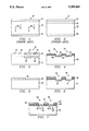
- FIG. 1 is a cross-sectional view of a wafer gettered using polysilicon backside gettering in accordance with the prior art
- FIG. 2 is cross-sectional view of a semiconductor wafer gettered using intrinsic oxygen precipitation gettering in accordance with the prior art
- FIG. 3 is a cross-sectional view of a device formed in accordance with the preferred embodiment of the present invention.
- FIG. 4 is a cross-sectional view illustrating the preferred method of the present invention.
- FIG. 5 is a cross-sectional view of an alternative embodiment of the method of the present invention.
- FIG. 6 is a cross-sectional view of a further alternative embodiment of the method in accordance with the present invention.
- FIG. 7 is a cross-sectional view of a still further alternative embodiment of the present invention.
- a cross-sectional view of a semiconductor wafer gettered in accordance with the prior art is generally identified by the reference numeral 10.
- the wafer 10 comprises a silicon substrate 12 with an epitaxial film 14 formed on one surface thereof.
- a polysilicon backside gettering layer 16 is formed on the opposite surface of the substrate 12.
- the devices that will make up integrated circuits on the wafer 10 will be formed in the epitaxial film layer 14.
- Epitaxial film layers comprise a very thin layer of silicon that is deposited on a silicon substrate, usually by chemical vapor deposition.
- the lattice structure of the epitaxial layer is identical to that of the silicon substrate and is formed to provide a layer with a different conductivity due to its relative purity compared to the substrate.
- the active components of a semiconductor device are totally formed in the epitaxial layer.
- the polysilicon layer 16 acts as a getterer to attract impurities within the silicon substrate 12, as well as any impurities that may be picked up during the various processes necessary to form integrated circuits on the wafer 10.
- the impurities diffuse through the substrate 12 toward the polysilicon layer 16, as indicated by arrows 18. If the substrate 12 is relatively thin, backside gettering may be sufficiently effective. However, if the substrate 12 becomes thicker due to an increased wafer diameter, the effectiveness of backside gettering is reduced and problems may occur with premature latch-up or loss of device lifetime.
- a semiconductor wafer gettered in accordance with the prior art method of intrinsic oxygen precipitation is generally identified by the reference numeral 20.
- the wafer 20 comprises a silicon substrate 22 and an epitaxial film layer 24, formed thereon subsequent to the oxygen precipitation gettering cycle.
- the wafer 20 is placed in a thermal oven for a standard high-low-high temperature cycle to produce oxygen precipitation denuded areas 26.
- the denuded areas 26 are relatively cleared of contaminants by the temperature cycling.
- the silicon substrate 22 is relatively thick, and processing temperatures are relatively low, intrinsic oxygen precipitation gettering to the center of the wafer thickness, becomes less effective and problems may occur with premature latch-up or loss of device lifetime.
- a semiconductor wafer constructed in accordance with the preferred embodiment of the present invention is generally identified by the reference numeral 30.
- the wafer 30 comprises a silicon substrate 32 and an epitaxial film layer 34.
- gettering areas 36 and 38 are formed in accordance with the present invention, as will be subsequently described in greater detail.
- a hydrochloric acid vapor etch may be conducted in situ to remove surface contaminants.
- Devices 40, 42, 44 and 46 Formed within the epitaxial layer 34 are integrated circuit devices, such as devices 40, 42, 44 and 46.
- Devices 44 and 46 which may be, for example, memory devices, require relatively high lifetime and are, therefore, gettered to remove contaminants by the corresponding proximity gettering areas 36 and 38.
- the devices 40 and 42 which may be high-speed switching devices, require lower lifetime and, therefore, do not need to be gettered but may need deliberate lifetime reduction.
- the gettering areas 36 and 38 form a lattice mismatch between the silicon substrate 32 and the epitaxial layer 34 as opposed to the normal matching of lattices.
- Testing as disclosed in Bean, et al., Germanium Doped Silicon Misfit Dislocation Gettering and Strain Layer Superlattice Structures via Conventional CVD Epitaxy, Electrochemical Society Vol. 88-1 (May 15-20, 1988), which is incorporated herein by reference, has shown that a material such as, for example, germanium, due to differences in the covalent radii of silicon and germanium (1.17 Angstroms vs. 1.22 Angstroms, respectively), will cause sufficient strain to provide lattice mismatch therebetween.
- the degree of strain is a function of the percentage of germanium to silicon and has been found through testing to be preferable at 1.5%-2.0%.
- the lattice mismatch thus formed between germanium areas 36 and 38 of the silicon substrate 32 and the silicon epitaxial layer 34 causes a lattice mismatch dislocation strain field. Contaminants are gettered to the lattice mismatch dislocations at gettering areas 36 and 38.
- the mismatch dislocation strain field may be created by the addition of atoms which have a substantially different (larger or smaller) ionic radius than that of silicon.
- the following elements are other examples of possible sources: boron, aluminium, gallium, tin, phosphorus, arsenic and antimony.
- a silicon semiconductor substrate 48 is processed in accordance with the preferred method of the present invention.
- a photoresist layer 50 is applied over a surface of the silicon substrate 48 and is masked and patterned using standard photolithographic processes, as are well known in the art, to form recesses 52 and 54 therein.
- the exposed silicon substrate 48 is then etched to form recesses 56 and 58 therein.
- Layers 60 and 62 of germanium-doped silicon are selectively deposited to fill the recesses 56 and 58.
- the photoresist 50 may then be stripped using a solvent based stripper.
- An epitaxial film layer (not shown) may be formed over the silicon substrate 48 and the germanium-doped silicon layers 60 and 62. Integrated circuit devices are then processed in the expitaxial film.
- the germanium-doped silicon preferably comprises 1.5%-2.0% germanium which is sufficient to cause a slight lattice mismatch between the substrate 48 and the subsequently applied epitaxial layer.
- the lattice mismatch produces dislocations which serve to getter impurities in the substrate 48 and process induced impurities away from the circuit devices formed proximate the layers 60-62.
- a silicon substrate 64 is completely covered with a germanium-doped silicon layer 66 which preferably comprises 1.5%-2.0% germanium.
- the layer 66 may then be patterned using standard photolithographic techniques and unwanted portions thereof etched to form ungettered areas such as area 68.
- planarization is a concern, the planarization of the surface may be re-established by a standard boron/phosphorus/glass (BPSG) application, as is well known in the art.
- BPSG boron/phosphorus/glass
- the layer 66 provides a slight lattice mismatch dislocation strain field between a subsequently applied epitaxial layer (not shown) and the silicon substrate 64 to getter impurities from selected area devices formed in the epitaxial layer.
- a silicon semiconductor substrate 70 is patterned using standard photolighographic processes to form recesses 72 and 74 in a photoresist layer 76.
- a standard ion-implantation is then used to implant germanium into the photoresist 76 and the exposed silicon semiconductor substrate 70 within the recesses 72 and .4, as illustrated by areas 78 and 80.
- a standard photoresist strip is then performed to remove the photoresist 76 and the ion-implantation thereon.
- the germanium implanted into the areas 78 and 80 is preferably at a concentration of 1.5%-2.0% germanium to silicon to form sufficient lattice mismatch between the substrate 70 and a subsequently applied epitaxial layer (not shown) to getter contaminants.
- a silicon semiconductor substrate 82 is masked, using standard photolithographic processes to form recesses 84 and 86 within a photoresist layer 88.
- Germanium as indicated at 90-92 is then deposited over the entire surface to cover the photoresist 88, as well as the exposed silicon substrate 82 within recesses 84 and 86.
- a standard thermal processing in a diffusion oven is conducted to diffuse the germanium 92 in the recesses 84 and 86 into the silicon substrate 82, as illustrated by arrows 94 and 96.
- the germanium 90-92 is preferably deposited to form a 1.5%-2.0% concentration with the silicon substrate 82 to form a slight lattice mismatch between the substrate 82 and a subsequently applied epitaxial layer (not shown). Contaminants will be selectively gettered from the substrate 82 to the germanium-doped silicon and away from any devices formed in the epitaxial layer.
- Integrated circuit devices which are formed in the subsequently applied epitaxial layer may thus be selectively gettered or ungettered. If long lifetime is desired for a circuit device such as a memory device, a mismatch strain field in accordance with the present invention may be formed proximate the device to getter any contaminants.
- short lifetime devices such as high-speed switches are positioned proximate the long lifetime devices, the short lifetime devices will be unaffected by the lattice mismatch strain fields.
- short and long lifetime devices may be effectively positioned proximate each other in the same layer of construction without interference from divergent gettering requirements.
- tin (Sn) is another Group IV element that may be used to produce the desired strain fields and not effect the conductivity or type of the silicon semiconductor. It is intended that the present invention encompass such changes and modifications as fall within the scope of the appended claims.
Abstract
A semiconductor wafer (32) is patterned to have gettering areas (36-38) selectively positioned proximate devices (44-46) which require gettering. The areas (36-38) comprise germanium-doped silicon having a germanium concentration of approximately 1.5%-2.0%. The germanium creates a lattice mismatch between the substrate (32) and an epitaxial layer (34) which is sufficient to produce defects capable of gettering contaminants. The gettering areas (36-38) may be formed by selective deposition, selective etching, ion-implantation or selective diffusion techniques.
Description
This application is a continuation of U.S. patent application Ser. No. 07/560,473, filed Jul. 27, 1990, now abandoned, which is a continuation of U.S. Pat. Ser. No. 287,743, filed Dec. 20, 1988, now abandoned.
This invention relates in general to semiconductor devices and processing, and in particular to a method for the discretionary gettering of semiconductor devices and devices formed thereby.
Silicon semiconductor substrates, which are used to manufacture integrated circuits, are susceptible to contamination from the diffusion of impurities. The contaminants may come from a surface material upon which the wafer is placed for processing or from any of the many processes to which the wafer is subjected. The contaminants may be picked up from the backside or the frontside of the wafer and may diffuse therethrough in either direction. The contaminants, which typically are heavy metals such as gold, copper, iron, nickel, etc., may show up on a surface of the wafer as a haze which is visible to the human eye.
Contaminants may, however, be both beneficial and detrimental to the integrated circuits being formed on the semiconductor wafer. Contaminants may cause low lifetime or high leakage current. Thus contaminants are not desirable wherever high lifetime is sought, such as in memory-type semiconductor devices. Whenever high lifetime is desired, contaminants must be gettered away from the device by some type of gettering method. Conversely, for example, in high speed switching devices, low lifetime is desired and therefore, contaminants do not need to be gettered.
Typical gettering methods currently in use include backside gettering, intrinsic oxygen precipitation gettering or a combination of backside and intrinsic oxygen precipitation gettering. In backside gettering, mechanical abrasions, silicon nitride, high phosphorus concentration, or a polysilicon layer is applied to the backside of the semiconductor wafer. These materials serve as an effective sink for contaminants in the wafer which are diffused through the thickness thereof. In oxygen precipitation gettering, the wafer is processed through a high temperature-low temperature-high temperature cycle to produce denuded zones near the top and bottom surfaces of the wafer which are relatively clear of contaminants, oxygen precipitates and other defects congregate in the center portion of the wafer and act as gettering sites.
The trend in semiconductor processing is toward lower processing temperatures and layer diameter, thus thicker wafers. Unfortunately, the thicker a substrate becomes, the less effective backside gettering becomes. Likewise, intrinsic oxygen precipitation gettering becomes less effective with lower processing temperatures. Thus, there is a need for a method to effectively getter a relatively thick substrate at relatively lower processing temperatures, as well as to discretionarily getter devices formed thereon.
The present invention disclosed herein comprises a method for discretionarily (or localized) gettering semiconductor circuits which substantially reduces or eliminates problems with prior gettering methods. The present invention allows the formation of improved semiconductor circuits by selectively gettering contaminants from a semiconductor substrate.
In accordance with one aspect of the invention, a semiconductor wafer is gettered. A mismatch dislocation strain field is formed over the semiconductor wafer by depositing a germanium-doped silicon film thereon. A subsequent epitaxial film in which integrated circuits are to be formed is deposited over the strain field. The strain field acts as a getterer for contaminants and is in near proximity to the active devices.
In a further aspect of the present invention, the germanium-doped silicon film comprises a molar concentration of 1.5%-2.0% germanium. The film may be deposited by selective deposition, uniform deposition followed by etching, ion-implantation or diffusion techniques.
In a still further aspect of the present invention, semiconductor devices may be selectively gettered or ungettered. A long lifetime device such as a memory circuit may be gettered to remove lifetime killing contaminants. A short lifetime device such as a high-speed switching device may be placed adjacent the long lifetime device without gettering contaminants therefrom. The method in accordance with the present invention allows the selective positioning of gettering areas not possible in the prior art.
It is a technical advantage of the present invention that a semiconductor substrate may be effectively gettered on a selective basis. It is possible to position a gettered area proximate a specific integrated circuit device to prevent latch-up or to provide enhanced device lifetime.
For a more complete understanding of the present invention and for further advantages thereof, reference is now made to the following Detailed Description taken in conjunction with the accompanying Drawings, in which:
FIG. 1 is a cross-sectional view of a wafer gettered using polysilicon backside gettering in accordance with the prior art;
FIG. 2 is cross-sectional view of a semiconductor wafer gettered using intrinsic oxygen precipitation gettering in accordance with the prior art;
FIG. 3 is a cross-sectional view of a device formed in accordance with the preferred embodiment of the present invention;
FIG. 4 is a cross-sectional view illustrating the preferred method of the present invention;
FIG. 5 is a cross-sectional view of an alternative embodiment of the method of the present invention;
FIG. 6 is a cross-sectional view of a further alternative embodiment of the method in accordance with the present invention; and
FIG. 7 is a cross-sectional view of a still further alternative embodiment of the present invention.
Referring to FIG. 1, a cross-sectional view of a semiconductor wafer gettered in accordance with the prior art is generally identified by the reference numeral 10. The wafer 10 comprises a silicon substrate 12 with an epitaxial film 14 formed on one surface thereof. On the opposite surface of the substrate 12, fox example, a polysilicon backside gettering layer 16 is formed. The devices that will make up integrated circuits on the wafer 10 will be formed in the epitaxial film layer 14.
Epitaxial film layers comprise a very thin layer of silicon that is deposited on a silicon substrate, usually by chemical vapor deposition. The lattice structure of the epitaxial layer is identical to that of the silicon substrate and is formed to provide a layer with a different conductivity due to its relative purity compared to the substrate. Typically, the active components of a semiconductor device are totally formed in the epitaxial layer.
The polysilicon layer 16 acts as a getterer to attract impurities within the silicon substrate 12, as well as any impurities that may be picked up during the various processes necessary to form integrated circuits on the wafer 10. The impurities diffuse through the substrate 12 toward the polysilicon layer 16, as indicated by arrows 18. If the substrate 12 is relatively thin, backside gettering may be sufficiently effective. However, if the substrate 12 becomes thicker due to an increased wafer diameter, the effectiveness of backside gettering is reduced and problems may occur with premature latch-up or loss of device lifetime.
Referring to FIG. 2, a semiconductor wafer gettered in accordance with the prior art method of intrinsic oxygen precipitation is generally identified by the reference numeral 20. The wafer 20 comprises a silicon substrate 22 and an epitaxial film layer 24, formed thereon subsequent to the oxygen precipitation gettering cycle.
The wafer 20 is placed in a thermal oven for a standard high-low-high temperature cycle to produce oxygen precipitation denuded areas 26. The denuded areas 26 are relatively cleared of contaminants by the temperature cycling. When the silicon substrate 22 is relatively thick, and processing temperatures are relatively low, intrinsic oxygen precipitation gettering to the center of the wafer thickness, becomes less effective and problems may occur with premature latch-up or loss of device lifetime.
Referring to FIG. 3, a semiconductor wafer constructed in accordance with the preferred embodiment of the present invention is generally identified by the reference numeral 30. The wafer 30 comprises a silicon substrate 32 and an epitaxial film layer 34. Within the silicon substrate 32 at the interface between the epitaxial layer 34 and substrate 32 are gettering areas 36 and 38 which are formed in accordance with the present invention, as will be subsequently described in greater detail. Prior to the formation of the layer 34, a hydrochloric acid vapor etch may be conducted in situ to remove surface contaminants.
Formed within the epitaxial layer 34 are integrated circuit devices, such as devices 40, 42, 44 and 46. Devices 44 and 46, which may be, for example, memory devices, require relatively high lifetime and are, therefore, gettered to remove contaminants by the corresponding proximity gettering areas 36 and 38. The devices 40 and 42, which may be high-speed switching devices, require lower lifetime and, therefore, do not need to be gettered but may need deliberate lifetime reduction.
The gettering areas 36 and 38 form a lattice mismatch between the silicon substrate 32 and the epitaxial layer 34 as opposed to the normal matching of lattices. Testing, as disclosed in Bean, et al., Germanium Doped Silicon Misfit Dislocation Gettering and Strain Layer Superlattice Structures via Conventional CVD Epitaxy, Electrochemical Society Vol. 88-1 (May 15-20, 1988), which is incorporated herein by reference, has shown that a material such as, for example, germanium, due to differences in the covalent radii of silicon and germanium (1.17 Angstroms vs. 1.22 Angstroms, respectively), will cause sufficient strain to provide lattice mismatch therebetween. The degree of strain is a function of the percentage of germanium to silicon and has been found through testing to be preferable at 1.5%-2.0%. The lattice mismatch thus formed between germanium areas 36 and 38 of the silicon substrate 32 and the silicon epitaxial layer 34 causes a lattice mismatch dislocation strain field. Contaminants are gettered to the lattice mismatch dislocations at gettering areas 36 and 38.
The mismatch dislocation strain field may be created by the addition of atoms which have a substantially different (larger or smaller) ionic radius than that of silicon. Thus, the following elements are other examples of possible sources: boron, aluminium, gallium, tin, phosphorus, arsenic and antimony.
Referring to FIG. 4, a silicon semiconductor substrate 48 is processed in accordance with the preferred method of the present invention. A photoresist layer 50 is applied over a surface of the silicon substrate 48 and is masked and patterned using standard photolithographic processes, as are well known in the art, to form recesses 52 and 54 therein. The exposed silicon substrate 48 is then etched to form recesses 56 and 58 therein.
The germanium-doped silicon preferably comprises 1.5%-2.0% germanium which is sufficient to cause a slight lattice mismatch between the substrate 48 and the subsequently applied epitaxial layer. The lattice mismatch produces dislocations which serve to getter impurities in the substrate 48 and process induced impurities away from the circuit devices formed proximate the layers 60-62.
Referring to FIG. 5, an alternative method in accordance with the present invention of forming gettering areas is illustrated. A silicon substrate 64 is completely covered with a germanium-doped silicon layer 66 which preferably comprises 1.5%-2.0% germanium. The layer 66 may then be patterned using standard photolithographic techniques and unwanted portions thereof etched to form ungettered areas such as area 68.
If planarization is a concern, the planarization of the surface may be re-established by a standard boron/phosphorus/glass (BPSG) application, as is well known in the art. The layer 66 provides a slight lattice mismatch dislocation strain field between a subsequently applied epitaxial layer (not shown) and the silicon substrate 64 to getter impurities from selected area devices formed in the epitaxial layer.
Referring to FIG. 6, a further alternative embodiment of the present invention is illustrated. A silicon semiconductor substrate 70 is patterned using standard photolighographic processes to form recesses 72 and 74 in a photoresist layer 76. A standard ion-implantation, as is well known in the art, is then used to implant germanium into the photoresist 76 and the exposed silicon semiconductor substrate 70 within the recesses 72 and .4, as illustrated by areas 78 and 80.
A standard photoresist strip is then performed to remove the photoresist 76 and the ion-implantation thereon. The germanium implanted into the areas 78 and 80 is preferably at a concentration of 1.5%-2.0% germanium to silicon to form sufficient lattice mismatch between the substrate 70 and a subsequently applied epitaxial layer (not shown) to getter contaminants.
Referring to FIG. 7, a still further alternative embodiment of the present invention is illustrated. A silicon semiconductor substrate 82 is masked, using standard photolithographic processes to form recesses 84 and 86 within a photoresist layer 88. Germanium as indicated at 90-92 is then deposited over the entire surface to cover the photoresist 88, as well as the exposed silicon substrate 82 within recesses 84 and 86.
A standard thermal processing in a diffusion oven is conducted to diffuse the germanium 92 in the recesses 84 and 86 into the silicon substrate 82, as illustrated by arrows 94 and 96. The germanium 90-92 is preferably deposited to form a 1.5%-2.0% concentration with the silicon substrate 82 to form a slight lattice mismatch between the substrate 82 and a subsequently applied epitaxial layer (not shown). Contaminants will be selectively gettered from the substrate 82 to the germanium-doped silicon and away from any devices formed in the epitaxial layer.
Integrated circuit devices which are formed in the subsequently applied epitaxial layer may thus be selectively gettered or ungettered. If long lifetime is desired for a circuit device such as a memory device, a mismatch strain field in accordance with the present invention may be formed proximate the device to getter any contaminants.
If short lifetime devices such as high-speed switches are positioned proximate the long lifetime devices, the short lifetime devices will be unaffected by the lattice mismatch strain fields. Thus, short and long lifetime devices may be effectively positioned proximate each other in the same layer of construction without interference from divergent gettering requirements.
Although the present invention as been described with respect to specific preferred embodiments thereof, various changes and modifications may be suggested to one skilled in the art (for example, tin (Sn) is another Group IV element that may be used to produce the desired strain fields and not effect the conductivity or type of the silicon semiconductor). It is intended that the present invention encompass such changes and modifications as fall within the scope of the appended claims.
Claims (18)
1. A method for forming an integrated circuit having a multiplicity of devices, comprising the steps of:
providing a silicon substrate;
introducing germanium atoms into selected areas of a surface of said substrate to form gettering areas, wherein said gettering areas have a molar concentration of between about 1.5% and 2.0% of germanium to germanium-doped silicon;
forming a crystalline semiconductor layer on said surface of said silicon substrate such that a lattice mismatch strain field exists between said gettering areas of said substrate and said crystalline layer; and
forming at least some of said multiplicity of devices in said crystalline layer, selected ones of said at least some devices disposed proximate said gettering areas having a lattice mismatch and at a surface of said crystalline layer spaced from said gettering areas such that contaminants migrate to said gettering areas and forming at least some others of said multiplicity of devices in said crystalline layer, said some others of said multiplicity of devices disposed such that contaminants are not substantially gettered from said some others of said multiplicity of devices.
2. A method as in claim 11 wherein said introducing of germanium atoms is performed by ion implantation.
3. A method as in claim 2 wherein said ion implantation is performed through a mask to provide selected areas where said germanium is introduced into said substrate.
4. The method of claim 1, wherein the step of forming said gettering areas comprises:
depositing a germanium-doped silicon film over the wafer; and
selectively etching said film to form gettered areas with said film and ungettered areas without said film.
5. The method of claim 1, wherein the step of forming said gettering areas comprises selectively diffusing germanium into the wafer.
6. A method for forming an integrated circuit in a silicon layer formed on a silicon substrate, said integrated circuit having at least one device of a multiplicity of devices formed proximate a gettering area formed in said substrate, said method comprising the steps of:
providing a silicon substrate;
introducing germanium atoms to form at least one gettering area within said substrate at a selected location, wherein said gettering area has a molar concentration of between about 1.5% and 2.0% of germanium to germanium-doped silicon; and
forming said at least one device in said silicon layer and selectively spaced from said selected location such that said gettering area attracts contaminants away from said at least one device and forming at least one other device in said silicon layer and selectively spaced form said selected location such that said gettering area does not substantially attract contaminants away from said at least one other device.
7. A method as in claim 6 wherein said introducing of germanium atoms is performed by ion implantation.
8. A method as in claim 7 wherein said ion implantation is performed through a mask to provide selected areas where said germanium is introduced into said substrate.
9. The method of claim 6, wherein said gettering area is formed by depositing a germanium-doped silicon film over the wafer.
10. The method of claim 9, wherein the step of depositing further comprises selectively depositing said film.
11. The method of claim 10, wherein the step of selectively depositing comprises;
patterning photoresist on the wafer;
forming recesses within the wafer corresponding to said pattern;
depositing said filming said recesses; and
stripping said photoresist.
12. The method of claim 9, further comprising the step of selectively etching said film.
13. The method of claim 12, wherein the step of selectively etching comprises:
masking said film with a photoresist pattern; and
etching said film to form gettered and ungettered areas.
14. The method of claim 13, further comprising the step of replanarizing the wafer with a boron/phosphorus/glass application.
15. The method of claim 6, wherein the step of forming said at least one gettering area comprises selectively diffusing germanium into the wafer.
16. The method of claim 6, wherein the step of forming gettering areas comprises:
masking the substrate to form gettered areas and ungettered areas;
etching the substrate to form recesses therein in said gettered areas;
depositing a germanium-doped silicon film in said recesses in said gettered areas; and
stripping said mask from said ungettered areas.
17. The method of claim 16, wherein the step of masking comprises forming an oxide over said ungettered areas.
18. The method of claim 16, wherein the step of depositing comprises depositing a 1.5%-2.0% germanium-doped silicon film.
Priority Applications (1)
| Application Number | Priority Date | Filing Date | Title |
|---|---|---|---|
| US07/824,770 US5250445A (en) | 1988-12-20 | 1992-01-17 | Discretionary gettering of semiconductor circuits |
Applications Claiming Priority (3)
| Application Number | Priority Date | Filing Date | Title |
|---|---|---|---|
| US28774388A | 1988-12-20 | 1988-12-20 | |
| US56047390A | 1990-07-27 | 1990-07-27 | |
| US07/824,770 US5250445A (en) | 1988-12-20 | 1992-01-17 | Discretionary gettering of semiconductor circuits |
Related Parent Applications (1)
| Application Number | Title | Priority Date | Filing Date |
|---|---|---|---|
| US56047390A Continuation | 1988-12-20 | 1990-07-27 |
Publications (1)
| Publication Number | Publication Date |
|---|---|
| US5250445A true US5250445A (en) | 1993-10-05 |
Family
ID=27403748
Family Applications (1)
| Application Number | Title | Priority Date | Filing Date |
|---|---|---|---|
| US07/824,770 Expired - Lifetime US5250445A (en) | 1988-12-20 | 1992-01-17 | Discretionary gettering of semiconductor circuits |
Country Status (1)
| Country | Link |
|---|---|
| US (1) | US5250445A (en) |
Cited By (39)
| Publication number | Priority date | Publication date | Assignee | Title |
|---|---|---|---|---|
| US5506155A (en) * | 1993-06-18 | 1996-04-09 | Rohm Co., Ltd. | Method for manufacturing a substrate for semiconductor device using a selective gettering technique |
| US5554883A (en) * | 1990-04-28 | 1996-09-10 | Mitsubishi Denki Kabushiki Kaisha | Semiconductor device and manufacturing method therefor |
| EP0791957A2 (en) * | 1996-02-23 | 1997-08-27 | Nec Corporation | Semiconductor substrate and method of manufacturing the same |
| US5734195A (en) * | 1993-03-30 | 1998-03-31 | Sony Corporation | Semiconductor wafer for epitaxially grown devices having a sub-surface getter region |
| US5821158A (en) * | 1995-08-28 | 1998-10-13 | Nec Corporation | Substrate surface treatment method capable of removing a spontaneous oxide film at a relatively low temperature |
| EP0949689A2 (en) * | 1998-04-07 | 1999-10-13 | Sony Corporation | Epitaxial semiconductor substrate and manufacturing method thereof; manufacturing method of semiconductor device and of solid-state imaging device |
| US6043112A (en) * | 1996-07-25 | 2000-03-28 | International Rectifier Corp. | IGBT with reduced forward voltage drop and reduced switching loss |
| US6291321B1 (en) * | 1997-06-24 | 2001-09-18 | Massachusetts Institute Of Technology | Controlling threading dislocation densities in Ge on Si using graded GeSi layers and planarization |
| US20030034529A1 (en) * | 2000-12-04 | 2003-02-20 | Amberwave Systems Corporation | CMOS inverter and integrated circuits utilizing strained silicon surface channel MOSFETs |
| US6649480B2 (en) | 2000-12-04 | 2003-11-18 | Amberwave Systems Corporation | Method of fabricating CMOS inverter and integrated circuits utilizing strained silicon surface channel MOSFETs |
| US6703144B2 (en) | 2000-01-20 | 2004-03-09 | Amberwave Systems Corporation | Heterointegration of materials using deposition and bonding |
| US6703688B1 (en) | 2001-03-02 | 2004-03-09 | Amberwave Systems Corporation | Relaxed silicon germanium platform for high speed CMOS electronics and high speed analog circuits |
| US6713326B2 (en) | 2000-08-16 | 2004-03-30 | Masachusetts Institute Of Technology | Process for producing semiconductor article using graded epitaxial growth |
| US6724008B2 (en) | 2001-03-02 | 2004-04-20 | Amberwave Systems Corporation | Relaxed silicon germanium platform for high speed CMOS electronics and high speed analog circuits |
| US6723661B2 (en) | 2001-03-02 | 2004-04-20 | Amberwave Systems Corporation | Relaxed silicon germanium platform for high speed CMOS electronics and high speed analog circuits |
| US6864115B2 (en) | 2000-01-20 | 2005-03-08 | Amberwave Systems Corporation | Low threading dislocation density relaxed mismatched epilayers without high temperature growth |
| US20050104100A1 (en) * | 2002-06-26 | 2005-05-19 | Nikon Corporation | Solid-state image sensor |
| EP1533847A1 (en) * | 2002-06-26 | 2005-05-25 | Nikon Corporation | Solid imaging device |
| US6933518B2 (en) | 2001-09-24 | 2005-08-23 | Amberwave Systems Corporation | RF circuits including transistors having strained material layers |
| US6940089B2 (en) | 2001-04-04 | 2005-09-06 | Massachusetts Institute Of Technology | Semiconductor device structure |
| US6995430B2 (en) | 2002-06-07 | 2006-02-07 | Amberwave Systems Corporation | Strained-semiconductor-on-insulator device structures |
| US20060113603A1 (en) * | 2004-12-01 | 2006-06-01 | Amberwave Systems Corporation | Hybrid semiconductor-on-insulator structures and related methods |
| US7060632B2 (en) | 2002-03-14 | 2006-06-13 | Amberwave Systems Corporation | Methods for fabricating strained layers on semiconductor substrates |
| US7074623B2 (en) | 2002-06-07 | 2006-07-11 | Amberwave Systems Corporation | Methods of forming strained-semiconductor-on-insulator finFET device structures |
| US7122449B2 (en) | 2002-06-10 | 2006-10-17 | Amberwave Systems Corporation | Methods of fabricating semiconductor structures having epitaxially grown source and drain elements |
| US7217603B2 (en) | 2002-06-25 | 2007-05-15 | Amberwave Systems Corporation | Methods of forming reacted conductive gate electrodes |
| US7227176B2 (en) | 1998-04-10 | 2007-06-05 | Massachusetts Institute Of Technology | Etch stop layer system |
| US7307273B2 (en) | 2002-06-07 | 2007-12-11 | Amberwave Systems Corporation | Control of strain in device layers by selective relaxation |
| US7332417B2 (en) | 2003-01-27 | 2008-02-19 | Amberwave Systems Corporation | Semiconductor structures with structural homogeneity |
| US7335545B2 (en) | 2002-06-07 | 2008-02-26 | Amberwave Systems Corporation | Control of strain in device layers by prevention of relaxation |
| US7368308B2 (en) | 2002-08-23 | 2008-05-06 | Amberwave Systems Corporation | Methods of fabricating semiconductor heterostructures |
| US7393733B2 (en) | 2004-12-01 | 2008-07-01 | Amberwave Systems Corporation | Methods of forming hybrid fin field-effect transistor structures |
| US7504704B2 (en) | 2003-03-07 | 2009-03-17 | Amberwave Systems Corporation | Shallow trench isolation process |
| US7594967B2 (en) | 2002-08-30 | 2009-09-29 | Amberwave Systems Corporation | Reduction of dislocation pile-up formation during relaxed lattice-mismatched epitaxy |
| US7615829B2 (en) | 2002-06-07 | 2009-11-10 | Amberwave Systems Corporation | Elevated source and drain elements for strained-channel heterojuntion field-effect transistors |
| US7776697B2 (en) | 2001-09-21 | 2010-08-17 | Taiwan Semiconductor Manufacturing Company, Ltd. | Semiconductor structures employing strained material layers with defined impurity gradients and methods for fabricating same |
| RU2512258C1 (en) * | 2012-10-17 | 2014-04-10 | Федеральное государственное бюджетное научное учреждение "Технологический институт сверхтвердых и новых углеродных материалов" (ФГБНУ ТИСНУМ) | Method of production of efficient inner getter in monocrystalline location-free silicon plates |
| US8748292B2 (en) | 2002-06-07 | 2014-06-10 | Taiwan Semiconductor Manufacturing Company, Ltd. | Methods of forming strained-semiconductor-on-insulator device structures |
| US8822282B2 (en) | 2001-03-02 | 2014-09-02 | Taiwan Semiconductor Manufacturing Company, Ltd. | Methods of fabricating contact regions for FET incorporating SiGe |
Citations (16)
| Publication number | Priority date | Publication date | Assignee | Title |
|---|---|---|---|---|
| US3515956A (en) * | 1967-10-16 | 1970-06-02 | Ion Physics Corp | High-voltage semiconductor device having a guard ring containing substitutionally active ions in interstitial positions |
| US3874936A (en) * | 1972-06-27 | 1975-04-01 | Ibm | Method of gettering impurities in semiconductor devices introducing stress centers and devices resulting thereof |
| US3895965A (en) * | 1971-05-24 | 1975-07-22 | Bell Telephone Labor Inc | Method of forming buried layers by ion implantation |
| US3969744A (en) * | 1971-07-27 | 1976-07-13 | U.S. Philips Corporation | Semiconductor devices |
| US3976512A (en) * | 1975-09-22 | 1976-08-24 | Signetics Corporation | Method for reducing the defect density of an integrated circuit utilizing ion implantation |
| US4082571A (en) * | 1975-02-20 | 1978-04-04 | Siemens Aktiengesellschaft | Process for suppressing parasitic components utilizing ion implantation prior to epitaxial deposition |
| US4114256A (en) * | 1977-06-24 | 1978-09-19 | Bell Telephone Laboratories, Incorporated | Reliable metal-to-junction contacts in large-scale-integrated devices |
| JPS58154284A (en) * | 1982-03-10 | 1983-09-13 | Hitachi Ltd | Manufacture of semiconductor laser device |
| JPS59119761A (en) * | 1982-12-24 | 1984-07-11 | Toshiba Corp | Manufactuer of semiconductor device |
| EP0133954A1 (en) * | 1983-07-29 | 1985-03-13 | Kabushiki Kaisha Toshiba | A method for manufacturing a semiconductor device |
| US4567645A (en) * | 1983-09-16 | 1986-02-04 | International Business Machines Corporation | Method for forming a buried subcollector in a semiconductor substrate by ion implantation |
| JPS61166032A (en) * | 1985-01-17 | 1986-07-26 | Matsushita Electronics Corp | Semiconductor substrate |
| US4668304A (en) * | 1985-04-10 | 1987-05-26 | Eaton Corporation | Dopant gettering semiconductor processing by excimer laser |
| DD248224A1 (en) * | 1984-06-20 | 1987-07-29 | Univ Berlin Humboldt | METHOD FOR PRODUCING SEMICONDUCTOR COMPONENTS |
| US4885257A (en) * | 1983-07-29 | 1989-12-05 | Kabushiki Kaisha Toshiba | Gettering process with multi-step annealing and inert ion implantation |
| US5094963A (en) * | 1981-07-17 | 1992-03-10 | Fujitsu Limited | Process for producing a semiconductor device with a bulk-defect region having a nonuniform depth |
-
1992
- 1992-01-17 US US07/824,770 patent/US5250445A/en not_active Expired - Lifetime
Patent Citations (16)
| Publication number | Priority date | Publication date | Assignee | Title |
|---|---|---|---|---|
| US3515956A (en) * | 1967-10-16 | 1970-06-02 | Ion Physics Corp | High-voltage semiconductor device having a guard ring containing substitutionally active ions in interstitial positions |
| US3895965A (en) * | 1971-05-24 | 1975-07-22 | Bell Telephone Labor Inc | Method of forming buried layers by ion implantation |
| US3969744A (en) * | 1971-07-27 | 1976-07-13 | U.S. Philips Corporation | Semiconductor devices |
| US3874936A (en) * | 1972-06-27 | 1975-04-01 | Ibm | Method of gettering impurities in semiconductor devices introducing stress centers and devices resulting thereof |
| US4082571A (en) * | 1975-02-20 | 1978-04-04 | Siemens Aktiengesellschaft | Process for suppressing parasitic components utilizing ion implantation prior to epitaxial deposition |
| US3976512A (en) * | 1975-09-22 | 1976-08-24 | Signetics Corporation | Method for reducing the defect density of an integrated circuit utilizing ion implantation |
| US4114256A (en) * | 1977-06-24 | 1978-09-19 | Bell Telephone Laboratories, Incorporated | Reliable metal-to-junction contacts in large-scale-integrated devices |
| US5094963A (en) * | 1981-07-17 | 1992-03-10 | Fujitsu Limited | Process for producing a semiconductor device with a bulk-defect region having a nonuniform depth |
| JPS58154284A (en) * | 1982-03-10 | 1983-09-13 | Hitachi Ltd | Manufacture of semiconductor laser device |
| JPS59119761A (en) * | 1982-12-24 | 1984-07-11 | Toshiba Corp | Manufactuer of semiconductor device |
| US4885257A (en) * | 1983-07-29 | 1989-12-05 | Kabushiki Kaisha Toshiba | Gettering process with multi-step annealing and inert ion implantation |
| EP0133954A1 (en) * | 1983-07-29 | 1985-03-13 | Kabushiki Kaisha Toshiba | A method for manufacturing a semiconductor device |
| US4567645A (en) * | 1983-09-16 | 1986-02-04 | International Business Machines Corporation | Method for forming a buried subcollector in a semiconductor substrate by ion implantation |
| DD248224A1 (en) * | 1984-06-20 | 1987-07-29 | Univ Berlin Humboldt | METHOD FOR PRODUCING SEMICONDUCTOR COMPONENTS |
| JPS61166032A (en) * | 1985-01-17 | 1986-07-26 | Matsushita Electronics Corp | Semiconductor substrate |
| US4668304A (en) * | 1985-04-10 | 1987-05-26 | Eaton Corporation | Dopant gettering semiconductor processing by excimer laser |
Non-Patent Citations (12)
| Title |
|---|
| Germanium Doped Silicon Misfit Dislocation Gettering and Strain Layer Superlattice Structures via Conventional CVD Epitaxy, Electrochemical Society, vol. 88 1 (May 15 20, 1988), Kenneth E. Bean et al., pp. 1 22. * |
| Germanium Doped Silicon Misfit Dislocation Gettering and Strain Layer Superlattice Structures via Conventional CVD Epitaxy, Electrochemical Society, vol. 88-1 (May 15-20, 1988), Kenneth E. Bean et al., pp. 1-22. |
| Herzog et al., "X-Ray Investigation of Boron- and Germanium Doped Silicon Epitaxial Layers," J. Electrochem. Soc., vol. 131, No. 12, 1984, pp. 2969-2974. |
| Herzog et al., X Ray Investigation of Boron and Germanium Doped Silicon Epitaxial Layers, J. Electrochem. Soc., vol. 131, No. 12, 1984, pp. 2969 2974. * |
| Poponiak et al. "Gettering technique resulting in defect free devices", IBM Tech. Disc. Bull. vol. 16 No. 4, Sep. 1973, p. 1063. |
| Poponiak et al. Gettering technique resulting in defect free devices , IBM Tech. Disc. Bull. vol. 16 No. 4, Sep. 1973, p. 1063. * |
| Poponiak et al., "Gettering Utilizing Implant Damage and Highly Disordered Epitaxial Layer", IBM Tech. Disc. Bull., vol. 19, No. 6, Nov. 1976, pp. 2052-2053. |
| Poponiak et al., Gettering Utilizing Implant Damage and Highly Disordered Epitaxial Layer , IBM Tech. Disc. Bull., vol. 19, No. 6, Nov. 1976, pp. 2052 2053. * |
| Wolf et al. Silicon Processing for the VLSI Era, Lattice Press, Sunset Beach, Calif., 1986, pp. 516 518. * |
| Wolf et al. Silicon Processing for the VLSI Era, Lattice Press, Sunset Beach, Calif., 1986, pp. 516-518. |
| Wolf, "Silicon Processing for the VLSI Era", vol. 1, pp. 141-142, Lattice Press, 1986. |
| Wolf, Silicon Processing for the VLSI Era , vol. 1, pp. 141 142, Lattice Press, 1986. * |
Cited By (73)
| Publication number | Priority date | Publication date | Assignee | Title |
|---|---|---|---|---|
| US5554883A (en) * | 1990-04-28 | 1996-09-10 | Mitsubishi Denki Kabushiki Kaisha | Semiconductor device and manufacturing method therefor |
| US5578507A (en) * | 1990-04-28 | 1996-11-26 | Mitsubishi Denki Kabushiki Kaisha | Method of making a semiconductor device having buried doped and gettering layers |
| US5734195A (en) * | 1993-03-30 | 1998-03-31 | Sony Corporation | Semiconductor wafer for epitaxially grown devices having a sub-surface getter region |
| US5874348A (en) * | 1993-03-30 | 1999-02-23 | Sony Corporation | Semiconductor wafer and method of manufacturing same |
| US5506155A (en) * | 1993-06-18 | 1996-04-09 | Rohm Co., Ltd. | Method for manufacturing a substrate for semiconductor device using a selective gettering technique |
| US5821158A (en) * | 1995-08-28 | 1998-10-13 | Nec Corporation | Substrate surface treatment method capable of removing a spontaneous oxide film at a relatively low temperature |
| KR100273832B1 (en) * | 1996-02-23 | 2001-01-15 | 가네꼬 히사시 | Semiconductor substrate and manufacturing method thereof |
| EP0791957A2 (en) * | 1996-02-23 | 1997-08-27 | Nec Corporation | Semiconductor substrate and method of manufacturing the same |
| EP0791957A3 (en) * | 1996-02-23 | 1997-10-29 | Nec Corp | Semiconductor substrate and method of manufacturing the same |
| US6043112A (en) * | 1996-07-25 | 2000-03-28 | International Rectifier Corp. | IGBT with reduced forward voltage drop and reduced switching loss |
| US6291321B1 (en) * | 1997-06-24 | 2001-09-18 | Massachusetts Institute Of Technology | Controlling threading dislocation densities in Ge on Si using graded GeSi layers and planarization |
| US6876010B1 (en) | 1997-06-24 | 2005-04-05 | Massachusetts Institute Of Technology | Controlling threading dislocation densities in Ge on Si using graded GeSi layers and planarization |
| US7250359B2 (en) * | 1997-06-24 | 2007-07-31 | Massachusetts Institute Of Technology | Controlling threading dislocation densities in Ge on Si using graded GeSi layers and planarization |
| US7081410B2 (en) | 1997-06-24 | 2006-07-25 | Massachusetts Institute Of Technology | Controlling threading dislocation densities in Ge on Si using graded GeSi layers and planarization |
| EP0949689A3 (en) * | 1998-04-07 | 2000-06-14 | Sony Corporation | Epitaxial semiconductor substrate and manufacturing method thereof; manufacturing method of semiconductor device and of solid-state imaging device |
| US6344092B1 (en) | 1998-04-07 | 2002-02-05 | Sony Corporation | Epitaxial semiconductor substrate, manufacturing method thereof, manufacturing method of semiconductor device and manufacturing method of solid-state imaging device |
| EP0949689A2 (en) * | 1998-04-07 | 1999-10-13 | Sony Corporation | Epitaxial semiconductor substrate and manufacturing method thereof; manufacturing method of semiconductor device and of solid-state imaging device |
| US7227176B2 (en) | 1998-04-10 | 2007-06-05 | Massachusetts Institute Of Technology | Etch stop layer system |
| US6703144B2 (en) | 2000-01-20 | 2004-03-09 | Amberwave Systems Corporation | Heterointegration of materials using deposition and bonding |
| US6864115B2 (en) | 2000-01-20 | 2005-03-08 | Amberwave Systems Corporation | Low threading dislocation density relaxed mismatched epilayers without high temperature growth |
| US6921914B2 (en) | 2000-08-16 | 2005-07-26 | Massachusetts Institute Of Technology | Process for producing semiconductor article using graded epitaxial growth |
| US6713326B2 (en) | 2000-08-16 | 2004-03-30 | Masachusetts Institute Of Technology | Process for producing semiconductor article using graded epitaxial growth |
| US6737670B2 (en) | 2000-08-16 | 2004-05-18 | Massachusetts Institute Of Technology | Semiconductor substrate structure |
| US6649480B2 (en) | 2000-12-04 | 2003-11-18 | Amberwave Systems Corporation | Method of fabricating CMOS inverter and integrated circuits utilizing strained silicon surface channel MOSFETs |
| US6881632B2 (en) | 2000-12-04 | 2005-04-19 | Amberwave Systems Corporation | Method of fabricating CMOS inverter and integrated circuits utilizing strained surface channel MOSFETS |
| US20030034529A1 (en) * | 2000-12-04 | 2003-02-20 | Amberwave Systems Corporation | CMOS inverter and integrated circuits utilizing strained silicon surface channel MOSFETs |
| US7256142B2 (en) | 2001-03-02 | 2007-08-14 | Amberwave Systems Corporation | Relaxed SiGe platform for high speed CMOS electronics and high speed analog circuits |
| US6703688B1 (en) | 2001-03-02 | 2004-03-09 | Amberwave Systems Corporation | Relaxed silicon germanium platform for high speed CMOS electronics and high speed analog circuits |
| US8822282B2 (en) | 2001-03-02 | 2014-09-02 | Taiwan Semiconductor Manufacturing Company, Ltd. | Methods of fabricating contact regions for FET incorporating SiGe |
| US7501351B2 (en) | 2001-03-02 | 2009-03-10 | Amberwave Systems Corporation | Relaxed SiGe platform for high speed CMOS electronics and high speed analog circuits |
| US6723661B2 (en) | 2001-03-02 | 2004-04-20 | Amberwave Systems Corporation | Relaxed silicon germanium platform for high speed CMOS electronics and high speed analog circuits |
| US6724008B2 (en) | 2001-03-02 | 2004-04-20 | Amberwave Systems Corporation | Relaxed silicon germanium platform for high speed CMOS electronics and high speed analog circuits |
| US7348259B2 (en) | 2001-04-04 | 2008-03-25 | Massachusetts Institute Of Technology | Method of fabricating a semiconductor structure that includes transferring one or more material layers to a substrate and smoothing an exposed surface of at least one of the material layers |
| US6940089B2 (en) | 2001-04-04 | 2005-09-06 | Massachusetts Institute Of Technology | Semiconductor device structure |
| US7884353B2 (en) | 2001-09-21 | 2011-02-08 | Taiwan Semiconductor Manufacturing Company, Ltd. | Semiconductor structures employing strained material layers with defined impurity gradients and methods for fabricating same |
| US7776697B2 (en) | 2001-09-21 | 2010-08-17 | Taiwan Semiconductor Manufacturing Company, Ltd. | Semiconductor structures employing strained material layers with defined impurity gradients and methods for fabricating same |
| US7846802B2 (en) | 2001-09-21 | 2010-12-07 | Taiwan Semiconductor Manufacturing Company, Ltd. | Semiconductor structures employing strained material layers with defined impurity gradients and methods for fabricating same |
| US7906776B2 (en) | 2001-09-24 | 2011-03-15 | Taiwan Semiconductor Manufacturing Company, Ltd. | RF circuits including transistors having strained material layers |
| US7709828B2 (en) | 2001-09-24 | 2010-05-04 | Taiwan Semiconductor Manufacturing Company, Ltd. | RF circuits including transistors having strained material layers |
| US6933518B2 (en) | 2001-09-24 | 2005-08-23 | Amberwave Systems Corporation | RF circuits including transistors having strained material layers |
| US7259108B2 (en) | 2002-03-14 | 2007-08-21 | Amberwave Systems Corporation | Methods for fabricating strained layers on semiconductor substrates |
| US7060632B2 (en) | 2002-03-14 | 2006-06-13 | Amberwave Systems Corporation | Methods for fabricating strained layers on semiconductor substrates |
| US7259388B2 (en) | 2002-06-07 | 2007-08-21 | Amberwave Systems Corporation | Strained-semiconductor-on-insulator device structures |
| US7109516B2 (en) | 2002-06-07 | 2006-09-19 | Amberwave Systems Corporation | Strained-semiconductor-on-insulator finFET device structures |
| US7297612B2 (en) | 2002-06-07 | 2007-11-20 | Amberwave Systems Corporation | Methods for forming strained-semiconductor-on-insulator device structures by use of cleave planes |
| US7307273B2 (en) | 2002-06-07 | 2007-12-11 | Amberwave Systems Corporation | Control of strain in device layers by selective relaxation |
| US7838392B2 (en) | 2002-06-07 | 2010-11-23 | Taiwan Semiconductor Manufacturing Company, Ltd. | Methods for forming III-V semiconductor device structures |
| US7335545B2 (en) | 2002-06-07 | 2008-02-26 | Amberwave Systems Corporation | Control of strain in device layers by prevention of relaxation |
| US6995430B2 (en) | 2002-06-07 | 2006-02-07 | Amberwave Systems Corporation | Strained-semiconductor-on-insulator device structures |
| US8748292B2 (en) | 2002-06-07 | 2014-06-10 | Taiwan Semiconductor Manufacturing Company, Ltd. | Methods of forming strained-semiconductor-on-insulator device structures |
| US7074623B2 (en) | 2002-06-07 | 2006-07-11 | Amberwave Systems Corporation | Methods of forming strained-semiconductor-on-insulator finFET device structures |
| US7615829B2 (en) | 2002-06-07 | 2009-11-10 | Amberwave Systems Corporation | Elevated source and drain elements for strained-channel heterojuntion field-effect transistors |
| US7414259B2 (en) | 2002-06-07 | 2008-08-19 | Amberwave Systems Corporation | Strained germanium-on-insulator device structures |
| US7420201B2 (en) | 2002-06-07 | 2008-09-02 | Amberwave Systems Corporation | Strained-semiconductor-on-insulator device structures with elevated source/drain regions |
| US7588994B2 (en) | 2002-06-07 | 2009-09-15 | Amberwave Systems Corporation | Methods for forming strained-semiconductor-on-insulator device structures by mechanically inducing strain |
| US7122449B2 (en) | 2002-06-10 | 2006-10-17 | Amberwave Systems Corporation | Methods of fabricating semiconductor structures having epitaxially grown source and drain elements |
| US7439164B2 (en) | 2002-06-10 | 2008-10-21 | Amberwave Systems Corporation | Methods of fabricating semiconductor structures having epitaxially grown source and drain elements |
| US8129821B2 (en) | 2002-06-25 | 2012-03-06 | Taiwan Semiconductor Manufacturing Co., Ltd. | Reacted conductive gate electrodes |
| US7217603B2 (en) | 2002-06-25 | 2007-05-15 | Amberwave Systems Corporation | Methods of forming reacted conductive gate electrodes |
| US20050104100A1 (en) * | 2002-06-26 | 2005-05-19 | Nikon Corporation | Solid-state image sensor |
| EP1533847A1 (en) * | 2002-06-26 | 2005-05-25 | Nikon Corporation | Solid imaging device |
| US7470944B2 (en) | 2002-06-26 | 2008-12-30 | Nikon Corporation | Solid-state image sensor |
| EP1533847A4 (en) * | 2002-06-26 | 2007-02-21 | Nikon Corp | Solid imaging device |
| US7375385B2 (en) | 2002-08-23 | 2008-05-20 | Amberwave Systems Corporation | Semiconductor heterostructures having reduced dislocation pile-ups |
| US7368308B2 (en) | 2002-08-23 | 2008-05-06 | Amberwave Systems Corporation | Methods of fabricating semiconductor heterostructures |
| US7829442B2 (en) | 2002-08-23 | 2010-11-09 | Taiwan Semiconductor Manufacturing Company, Ltd. | Semiconductor heterostructures having reduced dislocation pile-ups and related methods |
| US7594967B2 (en) | 2002-08-30 | 2009-09-29 | Amberwave Systems Corporation | Reduction of dislocation pile-up formation during relaxed lattice-mismatched epitaxy |
| US7332417B2 (en) | 2003-01-27 | 2008-02-19 | Amberwave Systems Corporation | Semiconductor structures with structural homogeneity |
| US7504704B2 (en) | 2003-03-07 | 2009-03-17 | Amberwave Systems Corporation | Shallow trench isolation process |
| US20060113603A1 (en) * | 2004-12-01 | 2006-06-01 | Amberwave Systems Corporation | Hybrid semiconductor-on-insulator structures and related methods |
| US8183627B2 (en) | 2004-12-01 | 2012-05-22 | Taiwan Semiconductor Manufacturing Company, Ltd. | Hybrid fin field-effect transistor structures and related methods |
| US7393733B2 (en) | 2004-12-01 | 2008-07-01 | Amberwave Systems Corporation | Methods of forming hybrid fin field-effect transistor structures |
| RU2512258C1 (en) * | 2012-10-17 | 2014-04-10 | Федеральное государственное бюджетное научное учреждение "Технологический институт сверхтвердых и новых углеродных материалов" (ФГБНУ ТИСНУМ) | Method of production of efficient inner getter in monocrystalline location-free silicon plates |
Similar Documents
| Publication | Publication Date | Title |
|---|---|---|
| US5250445A (en) | Discretionary gettering of semiconductor circuits | |
| US4717681A (en) | Method of making a heterojunction bipolar transistor with SIPOS | |
| US4272880A (en) | MOS/SOS Process | |
| US5244819A (en) | Method to getter contamination in semiconductor devices | |
| KR940008728B1 (en) | Semiconductor device and manufacturing method thereof | |
| US4512073A (en) | Method of forming self-aligned contact openings | |
| US4945070A (en) | Method of making cmos with shallow source and drain junctions | |
| US4875085A (en) | Semiconductor device with shallow n-type region with arsenic or antimony and phosphorus | |
| US4791074A (en) | Method of manufacturing a semiconductor apparatus | |
| JPS61503064A (en) | Semiconductor integrated circuit gettered with phosphorus | |
| US6111325A (en) | Gettering regions and methods of forming gettering regions within a semiconductor wafer | |
| US4716451A (en) | Semiconductor device with internal gettering region | |
| EP0051534B1 (en) | A method of fabricating a self-aligned integrated circuit structure using differential oxide growth | |
| US4498224A (en) | Method of manufacturing a MOSFET using accelerated ions to form an amorphous region | |
| US5087322A (en) | Selective metallization for high temperature semiconductors | |
| US4729967A (en) | Method of fabricating a junction field effect transistor | |
| US4409726A (en) | Method of making well regions for CMOS devices | |
| KR100294131B1 (en) | Process for fabricating semiconductor device without separation between silicide layer and insulating layer | |
| US4251300A (en) | Method for forming shaped buried layers in semiconductor devices utilizing etching, epitaxial deposition and oxide formation | |
| US4653173A (en) | Method of manufacturing an insulated gate field effect device | |
| US5284793A (en) | Method of manufacturing radiation resistant semiconductor device | |
| US5759869A (en) | Method to imporve metal step coverage by contact reflow | |
| KR960006689B1 (en) | Ldd manufacturing method of semiconductor device | |
| EP0078221A2 (en) | Polycrystalline silicon diode with metal silicide contact | |
| EP1035566A2 (en) | Method for forming a buried doped layer with connecting portions within a semiconductive device |
Legal Events
| Date | Code | Title | Description |
|---|---|---|---|
| STCF | Information on status: patent grant |
Free format text: PATENTED CASE |
|
| REMI | Maintenance fee reminder mailed | ||
| FPAY | Fee payment |
Year of fee payment: 4 |
|
| SULP | Surcharge for late payment | ||
| FPAY | Fee payment |
Year of fee payment: 8 |
|
| FPAY | Fee payment |
Year of fee payment: 12 |