US5159570A - Four memory state EEPROM - Google Patents
Four memory state EEPROM Download PDFInfo
- Publication number
- US5159570A US5159570A US07/697,228 US69722891A US5159570A US 5159570 A US5159570 A US 5159570A US 69722891 A US69722891 A US 69722891A US 5159570 A US5159570 A US 5159570A
- Authority
- US
- United States
- Prior art keywords
- gate
- sidewall
- programmed
- current
- state
- Prior art date
- Legal status (The legal status is an assumption and is not a legal conclusion. Google has not performed a legal analysis and makes no representation as to the accuracy of the status listed.)
- Expired - Lifetime
Links
- 230000015654 memory Effects 0.000 title claims abstract description 68
- 238000007667 floating Methods 0.000 claims abstract description 59
- 238000000034 method Methods 0.000 claims description 20
- 230000001939 inductive effect Effects 0.000 claims 2
- 239000004065 semiconductor Substances 0.000 description 12
- 239000000758 substrate Substances 0.000 description 12
- 230000008569 process Effects 0.000 description 6
- 238000000151 deposition Methods 0.000 description 4
- 239000002019 doping agent Substances 0.000 description 4
- 229910052785 arsenic Inorganic materials 0.000 description 3
- RQNWIZPPADIBDY-UHFFFAOYSA-N arsenic atom Chemical compound [As] RQNWIZPPADIBDY-UHFFFAOYSA-N 0.000 description 3
- 230000008021 deposition Effects 0.000 description 3
- 238000004519 manufacturing process Methods 0.000 description 3
- 230000005055 memory storage Effects 0.000 description 3
- 230000004044 response Effects 0.000 description 3
- OAICVXFJPJFONN-UHFFFAOYSA-N Phosphorus Chemical compound [P] OAICVXFJPJFONN-UHFFFAOYSA-N 0.000 description 2
- 230000008901 benefit Effects 0.000 description 2
- 230000015572 biosynthetic process Effects 0.000 description 2
- 230000005684 electric field Effects 0.000 description 2
- 230000006870 function Effects 0.000 description 2
- 239000007943 implant Substances 0.000 description 2
- 238000002347 injection Methods 0.000 description 2
- 239000007924 injection Substances 0.000 description 2
- 238000009413 insulation Methods 0.000 description 2
- 239000012212 insulator Substances 0.000 description 2
- 239000000463 material Substances 0.000 description 2
- 238000012986 modification Methods 0.000 description 2
- 230000004048 modification Effects 0.000 description 2
- 229910052698 phosphorus Inorganic materials 0.000 description 2
- 239000011574 phosphorus Substances 0.000 description 2
- XHXFXVLFKHQFAL-UHFFFAOYSA-N phosphoryl trichloride Chemical compound ClP(Cl)(Cl)=O XHXFXVLFKHQFAL-UHFFFAOYSA-N 0.000 description 2
- 229910052710 silicon Inorganic materials 0.000 description 2
- 239000010703 silicon Substances 0.000 description 2
- 238000003860 storage Methods 0.000 description 2
- 229910019213 POCl3 Inorganic materials 0.000 description 1
- 229910021417 amorphous silicon Inorganic materials 0.000 description 1
- QVGXLLKOCUKJST-UHFFFAOYSA-N atomic oxygen Chemical compound [O] QVGXLLKOCUKJST-UHFFFAOYSA-N 0.000 description 1
- 230000006399 behavior Effects 0.000 description 1
- 239000004020 conductor Substances 0.000 description 1
- 238000010276 construction Methods 0.000 description 1
- 238000005516 engineering process Methods 0.000 description 1
- 238000005530 etching Methods 0.000 description 1
- 239000002784 hot electron Substances 0.000 description 1
- 238000011065 in-situ storage Methods 0.000 description 1
- 238000005468 ion implantation Methods 0.000 description 1
- 150000002500 ions Chemical class 0.000 description 1
- 150000004767 nitrides Chemical class 0.000 description 1
- 229910052760 oxygen Inorganic materials 0.000 description 1
- 239000001301 oxygen Substances 0.000 description 1
- 229910021420 polycrystalline silicon Inorganic materials 0.000 description 1
- 239000003870 refractory metal Substances 0.000 description 1
- 229910021332 silicide Inorganic materials 0.000 description 1
- FVBUAEGBCNSCDD-UHFFFAOYSA-N silicide(4-) Chemical compound [Si-4] FVBUAEGBCNSCDD-UHFFFAOYSA-N 0.000 description 1
- 239000000243 solution Substances 0.000 description 1
Images

Classifications
-
- H—ELECTRICITY
- H10—SEMICONDUCTOR DEVICES; ELECTRIC SOLID-STATE DEVICES NOT OTHERWISE PROVIDED FOR
- H10B—ELECTRONIC MEMORY DEVICES
- H10B41/00—Electrically erasable-and-programmable ROM [EEPROM] devices comprising floating gates
- H10B41/30—Electrically erasable-and-programmable ROM [EEPROM] devices comprising floating gates characterised by the memory core region
-
- G—PHYSICS
- G11—INFORMATION STORAGE
- G11C—STATIC STORES
- G11C11/00—Digital stores characterised by the use of particular electric or magnetic storage elements; Storage elements therefor
- G11C11/56—Digital stores characterised by the use of particular electric or magnetic storage elements; Storage elements therefor using storage elements with more than two stable states represented by steps, e.g. of voltage, current, phase, frequency
- G11C11/5621—Digital stores characterised by the use of particular electric or magnetic storage elements; Storage elements therefor using storage elements with more than two stable states represented by steps, e.g. of voltage, current, phase, frequency using charge storage in a floating gate
- G11C11/5642—Sensing or reading circuits; Data output circuits
-
- G—PHYSICS
- G11—INFORMATION STORAGE
- G11C—STATIC STORES
- G11C16/00—Erasable programmable read-only memories
- G11C16/02—Erasable programmable read-only memories electrically programmable
- G11C16/04—Erasable programmable read-only memories electrically programmable using variable threshold transistors, e.g. FAMOS
- G11C16/0408—Erasable programmable read-only memories electrically programmable using variable threshold transistors, e.g. FAMOS comprising cells containing floating gate transistors
- G11C16/0441—Erasable programmable read-only memories electrically programmable using variable threshold transistors, e.g. FAMOS comprising cells containing floating gate transistors comprising cells containing multiple floating gate devices, e.g. separate read-and-write FAMOS transistors with connected floating gates
- G11C16/0458—Erasable programmable read-only memories electrically programmable using variable threshold transistors, e.g. FAMOS comprising cells containing floating gate transistors comprising cells containing multiple floating gate devices, e.g. separate read-and-write FAMOS transistors with connected floating gates comprising two or more independent floating gates which store independent data
-
- G—PHYSICS
- G11—INFORMATION STORAGE
- G11C—STATIC STORES
- G11C16/00—Erasable programmable read-only memories
- G11C16/02—Erasable programmable read-only memories electrically programmable
- G11C16/04—Erasable programmable read-only memories electrically programmable using variable threshold transistors, e.g. FAMOS
- G11C16/0466—Erasable programmable read-only memories electrically programmable using variable threshold transistors, e.g. FAMOS comprising cells with charge storage in an insulating layer, e.g. metal-nitride-oxide-silicon [MNOS], silicon-oxide-nitride-oxide-silicon [SONOS]
- G11C16/0475—Erasable programmable read-only memories electrically programmable using variable threshold transistors, e.g. FAMOS comprising cells with charge storage in an insulating layer, e.g. metal-nitride-oxide-silicon [MNOS], silicon-oxide-nitride-oxide-silicon [SONOS] comprising two or more independent storage sites which store independent data
-
- H—ELECTRICITY
- H01—ELECTRIC ELEMENTS
- H01L—SEMICONDUCTOR DEVICES NOT COVERED BY CLASS H10
- H01L21/00—Processes or apparatus adapted for the manufacture or treatment of semiconductor or solid state devices or of parts thereof
- H01L21/02—Manufacture or treatment of semiconductor devices or of parts thereof
- H01L21/04—Manufacture or treatment of semiconductor devices or of parts thereof the devices having at least one potential-jump barrier or surface barrier, e.g. PN junction, depletion layer or carrier concentration layer
- H01L21/18—Manufacture or treatment of semiconductor devices or of parts thereof the devices having at least one potential-jump barrier or surface barrier, e.g. PN junction, depletion layer or carrier concentration layer the devices having semiconductor bodies comprising elements of Group IV of the Periodic System or AIIIBV compounds with or without impurities, e.g. doping materials
- H01L21/28—Manufacture of electrodes on semiconductor bodies using processes or apparatus not provided for in groups H01L21/20 - H01L21/268
- H01L21/28008—Making conductor-insulator-semiconductor electrodes
- H01L21/28017—Making conductor-insulator-semiconductor electrodes the insulator being formed after the semiconductor body, the semiconductor being silicon
- H01L21/28026—Making conductor-insulator-semiconductor electrodes the insulator being formed after the semiconductor body, the semiconductor being silicon characterised by the conductor
- H01L21/28123—Lithography-related aspects, e.g. sub-lithography lengths; Isolation-related aspects, e.g. to solve problems arising at the crossing with the side of the device isolation; Planarisation aspects
- H01L21/2815—Lithography-related aspects, e.g. sub-lithography lengths; Isolation-related aspects, e.g. to solve problems arising at the crossing with the side of the device isolation; Planarisation aspects part or whole of the electrode is a sidewall spacer or made by a similar technique, e.g. transformation under mask, plating
-
- H—ELECTRICITY
- H01—ELECTRIC ELEMENTS
- H01L—SEMICONDUCTOR DEVICES NOT COVERED BY CLASS H10
- H01L29/00—Semiconductor devices adapted for rectifying, amplifying, oscillating or switching, or capacitors or resistors with at least one potential-jump barrier or surface barrier, e.g. PN junction depletion layer or carrier concentration layer; Details of semiconductor bodies or of electrodes thereof ; Multistep manufacturing processes therefor
- H01L29/40—Electrodes ; Multistep manufacturing processes therefor
- H01L29/401—Multistep manufacturing processes
- H01L29/4011—Multistep manufacturing processes for data storage electrodes
- H01L29/40114—Multistep manufacturing processes for data storage electrodes the electrodes comprising a conductor-insulator-conductor-insulator-semiconductor structure
-
- H—ELECTRICITY
- H01—ELECTRIC ELEMENTS
- H01L—SEMICONDUCTOR DEVICES NOT COVERED BY CLASS H10
- H01L29/00—Semiconductor devices adapted for rectifying, amplifying, oscillating or switching, or capacitors or resistors with at least one potential-jump barrier or surface barrier, e.g. PN junction depletion layer or carrier concentration layer; Details of semiconductor bodies or of electrodes thereof ; Multistep manufacturing processes therefor
- H01L29/40—Electrodes ; Multistep manufacturing processes therefor
- H01L29/41—Electrodes ; Multistep manufacturing processes therefor characterised by their shape, relative sizes or dispositions
- H01L29/423—Electrodes ; Multistep manufacturing processes therefor characterised by their shape, relative sizes or dispositions not carrying the current to be rectified, amplified or switched
- H01L29/42312—Gate electrodes for field effect devices
- H01L29/42316—Gate electrodes for field effect devices for field-effect transistors
- H01L29/4232—Gate electrodes for field effect devices for field-effect transistors with insulated gate
- H01L29/42324—Gate electrodes for transistors with a floating gate
-
- H—ELECTRICITY
- H01—ELECTRIC ELEMENTS
- H01L—SEMICONDUCTOR DEVICES NOT COVERED BY CLASS H10
- H01L29/00—Semiconductor devices adapted for rectifying, amplifying, oscillating or switching, or capacitors or resistors with at least one potential-jump barrier or surface barrier, e.g. PN junction depletion layer or carrier concentration layer; Details of semiconductor bodies or of electrodes thereof ; Multistep manufacturing processes therefor
- H01L29/66—Types of semiconductor device ; Multistep manufacturing processes therefor
- H01L29/68—Types of semiconductor device ; Multistep manufacturing processes therefor controllable by only the electric current supplied, or only the electric potential applied, to an electrode which does not carry the current to be rectified, amplified or switched
- H01L29/76—Unipolar devices, e.g. field effect transistors
- H01L29/772—Field effect transistors
- H01L29/78—Field effect transistors with field effect produced by an insulated gate
- H01L29/788—Field effect transistors with field effect produced by an insulated gate with floating gate
- H01L29/7881—Programmable transistors with only two possible levels of programmation
- H01L29/7884—Programmable transistors with only two possible levels of programmation charging by hot carrier injection
- H01L29/7885—Hot carrier injection from the channel
-
- H—ELECTRICITY
- H01—ELECTRIC ELEMENTS
- H01L—SEMICONDUCTOR DEVICES NOT COVERED BY CLASS H10
- H01L29/00—Semiconductor devices adapted for rectifying, amplifying, oscillating or switching, or capacitors or resistors with at least one potential-jump barrier or surface barrier, e.g. PN junction depletion layer or carrier concentration layer; Details of semiconductor bodies or of electrodes thereof ; Multistep manufacturing processes therefor
- H01L29/66—Types of semiconductor device ; Multistep manufacturing processes therefor
- H01L29/68—Types of semiconductor device ; Multistep manufacturing processes therefor controllable by only the electric current supplied, or only the electric potential applied, to an electrode which does not carry the current to be rectified, amplified or switched
- H01L29/76—Unipolar devices, e.g. field effect transistors
- H01L29/772—Field effect transistors
- H01L29/78—Field effect transistors with field effect produced by an insulated gate
- H01L29/788—Field effect transistors with field effect produced by an insulated gate with floating gate
- H01L29/7887—Programmable transistors with more than two possible different levels of programmation
-
- H—ELECTRICITY
- H10—SEMICONDUCTOR DEVICES; ELECTRIC SOLID-STATE DEVICES NOT OTHERWISE PROVIDED FOR
- H10B—ELECTRONIC MEMORY DEVICES
- H10B69/00—Erasable-and-programmable ROM [EPROM] devices not provided for in groups H10B41/00 - H10B63/00, e.g. ultraviolet erasable-and-programmable ROM [UVEPROM] devices
-
- G—PHYSICS
- G11—INFORMATION STORAGE
- G11C—STATIC STORES
- G11C2211/00—Indexing scheme relating to digital stores characterized by the use of particular electric or magnetic storage elements; Storage elements therefor
- G11C2211/56—Indexing scheme relating to G11C11/56 and sub-groups for features not covered by these groups
- G11C2211/561—Multilevel memory cell aspects
- G11C2211/5612—Multilevel memory cell with more than one floating gate
Definitions
- This invention relates to the field of electrically erasable programmable read only memory (EEPROM) semiconductor devices. Specifically, the present invention relates to an EEPROM cell having increased memory storage capabilities due to two floating gate structures contained within each cell.
- EEPROM electrically erasable programmable read only memory
- EEPROMs electrically erasable programmable read only memories
- EEPROMs often use a floating gate avalanche injection MOS (FAMOS) structure to store program information.
- FMOS floating gate avalanche injection MOS
- One solution to the problem of dimensioning a floating gate at minimum photolithographic limits is provided by the use of a single sidewall floating gate formed on a sidewall of the control gate.
- the resulting structure is generally no smaller than a conventional FAMOS structure and achieves no greater memory storage capabilities. Accordingly, a need exists for a memory cell in which a floating gate structure is used to increase the storage capacity of the memory cell while maintaining the size of the cell at an acceptably small magnitude.
- One aspect of the present invention comprises an EEPROM memory cell wherein the memory cell has a pair of sidewall floating gates formed adjacent the control gate.
- a technical advantage of the present invention is that this cell is capable of four distinct states and therefore can hold two bits of memory as opposed to the two distinct states and single bit storage capability of a conventional cell. Memory storage capabilities are doubled without a comparable increase in memory cell size.
- an EEPROM memory cell has first and second regions of one conductivity type formed on a semiconductor surface of a different conductivity type so that the first and second regions function as a source and drain for the memory cell.
- a channel region is defined between the first and second regions and is divided into three subregions.
- a central subregion is controlled by a control gate separated from the semiconductor surface by a control gate insulator.
- Two outside floating gate channel regions flanking the central region are controlled by sidewall floating gate filaments. These sidewall floating gate filaments may be programmed independently of each other and the cell may then be read using either the source or the drain to define four distinct memory states.
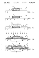
- FIGS. 1a through 1e are elevational schematic cross sectional views of successive processing steps for building a single EEPROM memory cell according to the present invention
- FIG. 2 is a plan view of a single EEPROM cell, in which line 1--1 corresponds to the cross section represented in FIGS. 1a through 1e;
- FIG. 3 is a flow chart showing the method used to read the memory state of the present invention.
- FIG. 4 shows voltage versus current curves applicable to read operations of the present invention.
- FIGS. 1a through 1e illustrate processing steps for the fabrication of an EEPROM memory array according to the present invention.
- a memory array contains a multiplicity of memory cells.
- all memory cells within a memory array are constructed as a result of the same process steps, and therefore, all cells are similar in structure. Consequently, an entire array (not shown) of memory cells is described herein by reference only to a single cell, indicated generally at 10, depicted in FIGS. 1a through 1e. It will be understood by those skilled in the art that many memory cells may reside on either side of the cells depicted in FIGS. 1a through 1e. In addition, many memory cells may reside both above and below the cells shown in FIGS. 1a through 1e in a direction perpendicular to the sectional plane shown.
- Memory cell 10 includes a (P) type semiconductor substrate 12 upon which the processing steps depicted in FIG. 1a are performed.
- a thin oxide layer 14 is formed at a semiconductor substrate surface 16 of substrate 12.
- Oxide layer 14 may advantageously be grown in a dry oxygen or steam environment at a temperature of approximately 900° C. until a thickness of approximately 350 Angstroms has been achieved.
- Oxide layer 14 initially covers the entire surface 16 of array 10 (initial state not shown).
- a layer 18 of polycrystalline or amorphous material comprising silicon is deposited on oxide layer 14. Layer 18 is formed to be of a thickness on the order of one micron.
- a second layer 20 of oxide is grown or deposited thereover.
- Block 22 includes control gate 18 disposed between oxide layers 14 and 20.
- Control gate 18 may comprise any one of a variety of conductive materials, for example, polycrystalline or amorphous silicon, refractory metals or silicide.
- Oxide layer 24 is grown over semiconductor substrate surface 16 and exposed nonoxide sidewall surfaces of central block 22.
- Oxide layer 24 is of a thickness on the order of 100 Angstroms.
- the next step is a conformal deposition of a second conductive layer 26 of polycrystalline or amorphous material comprising silicon.
- Conductive layer 26 is initially formed to be of a thickness on the order of 3000 Angstroms.
- second conductive layer 26 is doped in situ using POCl 3 , for example, and then anisotropically etched using an etchant which is selective to oxide.
- sidewall floating gate filaments 28a and 28b are formed on sidewalls 30 and 32 of central block 22.
- Sidewall floating gate filaments 28a and 28b are insulatively separated from substrate surface 16 of substrate 12 and from central block 22 by oxide layer 24.
- the thicker control gate 18 is formed, the better the control over sidewall floating gate filaments 28a and 28b due to the increased surface area of the sidewalls of control gate 18.
- Sidewall floating gate filaments 28a and 28b and central block 22 are disposed over the substrate surface 16 to define a channel region 34 of an EEPROM transistor.
- An ion implantation procedure then implants an (N+) dopant into substrate 12 adjacent each side of the channel region 34.
- N+ dopant any conventional (N+) dopant may be used, the preferred embodiment of the present invention uses arsenic at a concentration of approximately 5 ⁇ 10 15 atoms per square centimeter, and at an energy level of approximately 60 KeV.
- Arsenic is preferred over, for example, phosphorus because arsenic diffuses away from the area in which it is implanted less than phosphorus.
- bit lines 36a and 36b are formed in substrate 12 at substrate surface 16.
- Bit lines 36a and 36b function as sources and drains for memory cell transistors and extend the entire length of the memory array.
- the implant of the (N+) dopants may take place through oxide layer 24 due to its thin nature without requiring removal of oxide layer 24 from the selected bit line sites.
- the final cross sectional structure of the present memory cell is shown in FIG. 1e and is accomplished by the additional process steps of depositing an insulator oxide layer 38 and forming electrical contacts 40a and 40b therethrough to provide electrical connection with bit lines 36a and 36b.
- FIG. 2 A plan view of the memory cell is shown in FIG. 2 indicating a line 1--1 where the cross section shown in FIG. 1e is located.
- Control gate 18 may be seen to be centered in the memory cell, with oxide layers 24 extending along opposite sides of control gate 18.
- Sidewall floating gate filaments 28a and 28b are disposed between oxide layers 24 and bit lines 36a and 36b. Electrical contacts 40a and 40b extend over and into contact with bit lines 36a and 36b.
- Sidewall floating gates 28a and 28b are truncated and do not extend the full length of the control gate 18. This is done with mask and poly etch process steps after the sidewall filament formation.
- the sidewall floating gates 28a and 28b formed in this way are fully isolated and surrounded by oxide, and therefore can store electric charge.
- the memory cell 10 is programmed by causing hot electrons to be injected through gate oxide 24 into one of, both of or neither of the floating gates 28a and 28b. This injection of electrons occurs under the influence of a relatively strong electrical field. Once the strong electrical field has been removed, these electrons are trapped in floating gates 28a and 28b causing the memory cell to be programmed.
- Floating gates 28a and 28b may be programmed independently of one another. As a result, the memory cell may be programmed to store up to four distinct information states. For example, a first information state may be represented by leaving both of sidewall floating gates 28a and 28b unprogrammed. A second information state may be represented by programming only sidewall floating gate 28a and not sidewall floating gate 28b. A third information state may be represented by programming only sidewall floating gate 28b and not sidewall floating gate 28a, and a fourth information state may be represented by programming both sidewall floating gates 28a and 28b.
- Sidewall floating gate 28a is programmed by applying a zero volt potential to bit line 36a, which then acts as the drain of the memory cell. A relatively high positive voltage pulse is then applied on control gate 18. Bit line 36b is allowed to float to prevent the programming of sidewall floating gate 28b.
- floating gate 28b is programmed by applying a zero volt potential to bit line 36b and applying a relatively high voltage pulse to control gate 18.
- Bit line 36a is allowed to float to prevent the programming of sidewall floating gate 28a.
- Both of floating gates 28a and 28b within a memory cell may be programmed in two steps by first programming one of the sidewall floating gates 28a and 28b as discussed above, then programming the other of sidewall floating gates 28a and 28b.
- a particular memory cell is read by applying moderate voltages, such as in the range of 3 to 5 volts, to a particular source, drain and control gate that uniquely define the memory cell.
- FIG. 3 shows a graph of relationships between drain to source voltage levels and current levels which occur when reading a memory cell.
- the above described four distinct information states may be detected by sensing current flowing in the cell under various conditions.
- curve 42 represents the ability of memory cell 10 to conduct current during a read operation when neither of sidewall floating gates 28a and 28b are programmed. In this situation, memory cell 10 conducts a relatively large amount of current at a relatively low or moderate drain to source voltage potential and it makes no difference which of bit lines 36a and 36b are used as the source and drain for the read operation due to its symmetrical construction.
- a curve 44 shows the electrical behavior of memory cell 10 during a read operation when only sidewall floating gate 28a has been programmed and memory cell 10 is being read with bit line 36a serving as the drain. Curve 44 also depicts the relationship of voltage to current which results during a read operation when only sidewall floating gate 28b has been programmed and memory cell 10 is being read with bit line 36b serving as the drain. For both of these situations, memory cell 10 conducts a moderate amount of current when a moderate voltage potential is applied between its drain and source.
- a single curve 46 shown in FIG. 3 illustrates the performance of memory cell 10 during a read operation for each of three additional situations.
- the response illustrated by curve 46 occurs when both of sidewall floating gates 28a and 28b have been programmed and either bit line 36a or 36b is used as the drain during the read operation.
- This response also occurs when only sidewall floating gate 28a has been programmed and memory cell 10 is being read with bit line 36b serving as the drain.
- this response also occurs when only sidewall floating gate 28b has been programmed and memory cell 10 has been read with bit line 36a serving as the drain.
- a relatively low amount of current flows through memory cell 10 when a moderate voltage potential is applied between its drain and source.
- FIG. 4 illustrates the flow chart of a process whereby the state of memory cell 10 may be determined using two successive read operations.
- Memory cell 10 is capable of being in four distinct information states and can thereby store two bits of information. It is very difficult to distinguish between the high current level represented by curve 42 in FIG. 3 and the moderate current level represented by curve 44. Accordingly, using the process illustrated in FIG. 4, the state of memory cell 10 can be determined without having to make this difficult distinction.
- a first read step is performed on the memory cell 10 with either bit line 36a or 36b serving as the drain or "line A" as shown in block 50 on FIG. 4.
- a decision is made whether memory cell 10 is conducting a low amount of current or a high or moderate amount of current. If memory cell 10 is conducting a low amount of current, a second read operation occurs in block 54 using line B, the opposite bit line from that used in step 50 described above. Because a low amount of current was found in decision block 52, it is known that "gate B", the gate opposite from the bit line being read, is programmed and is storing charge. The second read operation is necessary to determine if gate A has been programmed and is storing charge.
- each state shown in block 54 represents the state of gate A and the second digit represents the state of gate B.
- a "0” represents that the gate is storing charge and a "1" represents that the gate is not storing charge.
- a second read operation is then performed at 62 using line B to determine whether gate A is storing charge. If a low amount of current is detected at decision block 64, gate A has been programmed and is storing charge. This indicates an information state "01" has been detected as shown in block 66. If a high amount of current is detected at 64, neither gate A nor B is storing charge and an information state "11" is indicated as shown in block 68. Using the process shown in FIG. 4, the four possible information states of memory cell 10 may be determined without having to distinguish between a high and a moderate amount of current.
- the memory cell of the present invention is wholly symmetrical. Therefore, although FIG. 4 shows that bit line "A" is read first in the "read” operation, either bit line may be read first with no detectable difference in performance. Hence, referring to FIG. 1e, either bit line 36a or 36b could be read first as line A in the read operation shown in FIG. 4.
- This symmetry provides an important technical advantage of the present invention in that the software necessary to perform the "read” operation may be designed with much greater flexibility.
- Sidewall floating gate 28b shown in FIG. 2 is electrically erased by holding the control gate 18 at ground potential and applying a relatively high voltage pulse to bit line 36b.
- Bit line 36a can be grounded or left floating while erasing sidewall floating gate 28b.
- Sidewall floating gate 28a is electrically erased in a similar manner by holding the control gate 18 at ground potential and applying a relatively high voltage pulse to bit line 36a.
- the present invention is capable of storing four distinct information states or two bits of information in an area comparable to the cell sizes of conventional memory cells manufactured by conventional photolithographic techniques.
- these dimensions reflect current processing capabilities and such dimensions may decrease as a result of improvements in semiconductor processing techniques.
- insulation layer 24 as being comprised of oxide.
- Insulation layer 24 may alternatively be formed of a dielectric comprising a first layer of oxide followed by a layer of nitride followed by a second layer of oxide forming a highly effective dielectric layer between sidewall floating gate filaments 28a and 28b and control gate structure 22 and substrate 12.
Abstract
An EEPROM memory cell having sidewall floating gates (28, 28a, 28b) is disclosed. Sidewall floating gates (28, 28a, 28b) are formed on sidewalls (30, 32) of a central block (22). Spaced apart bit lines (36, 36a, 36b) are formed to serve as memory cell sources and drains. Sidewall floating gates (28a, 28b) are capable of being programmed independently of one another. When control gate (18) is actuated and either bit line (36a) or bit line (36b) is used to read the device, four separate memory states may be identified depending on whether either, neither or both of the sidewall floating gates (28a, 28b) have been programmed.
Description
This is a division of application Ser. No. 07/288,497, filed Dec. 22, 1988, now abandoned, which is a continuation-in-part of Ser. No. 07/137,401, filed Dec. 23, 1987, abandoned.
This invention relates to the field of electrically erasable programmable read only memory (EEPROM) semiconductor devices. Specifically, the present invention relates to an EEPROM cell having increased memory storage capabilities due to two floating gate structures contained within each cell.
One of the goals in the fabrication of electrically erasable programmable read only memories (EEPROMs) is the production of memory circuits which are capable of storing a maximum amount of information using a minimum amount of semiconductor surface area. However, photolithographic limits imposed by conventional semiconductor processing technology impede the achievement of this goal. Thus, an inability to pattern and etch semiconductor features beyond current physical limits prevents a memory cell from being constructed having the desired minimum semiconductor surface area.
EEPROMs often use a floating gate avalanche injection MOS (FAMOS) structure to store program information. One solution to the problem of dimensioning a floating gate at minimum photolithographic limits is provided by the use of a single sidewall floating gate formed on a sidewall of the control gate. However, since such a floating gate is merely added to a sidewall of an ordinary photolithographically defined control gate, the resulting structure is generally no smaller than a conventional FAMOS structure and achieves no greater memory storage capabilities. Accordingly, a need exists for a memory cell in which a floating gate structure is used to increase the storage capacity of the memory cell while maintaining the size of the cell at an acceptably small magnitude.
One aspect of the present invention comprises an EEPROM memory cell wherein the memory cell has a pair of sidewall floating gates formed adjacent the control gate. A technical advantage of the present invention is that this cell is capable of four distinct states and therefore can hold two bits of memory as opposed to the two distinct states and single bit storage capability of a conventional cell. Memory storage capabilities are doubled without a comparable increase in memory cell size.
According to another aspect of the invention, an EEPROM memory cell has first and second regions of one conductivity type formed on a semiconductor surface of a different conductivity type so that the first and second regions function as a source and drain for the memory cell. A channel region is defined between the first and second regions and is divided into three subregions. A central subregion is controlled by a control gate separated from the semiconductor surface by a control gate insulator. Two outside floating gate channel regions flanking the central region are controlled by sidewall floating gate filaments. These sidewall floating gate filaments may be programmed independently of each other and the cell may then be read using either the source or the drain to define four distinct memory states.
A more complete understanding of the present invention may be acquired by referring to the detailed description and claims when considered in connection with the accompanying drawings, in which like reference numbers indicate like features throughout the drawings, and wherein:
FIGS. 1a through 1e are elevational schematic cross sectional views of successive processing steps for building a single EEPROM memory cell according to the present invention;
FIG. 2 is a plan view of a single EEPROM cell, in which line 1--1 corresponds to the cross section represented in FIGS. 1a through 1e;
FIG. 3 is a flow chart showing the method used to read the memory state of the present invention; and
FIG. 4 shows voltage versus current curves applicable to read operations of the present invention.
FIGS. 1a through 1e illustrate processing steps for the fabrication of an EEPROM memory array according to the present invention.
A memory array contains a multiplicity of memory cells. Typically, all memory cells within a memory array are constructed as a result of the same process steps, and therefore, all cells are similar in structure. Consequently, an entire array (not shown) of memory cells is described herein by reference only to a single cell, indicated generally at 10, depicted in FIGS. 1a through 1e. It will be understood by those skilled in the art that many memory cells may reside on either side of the cells depicted in FIGS. 1a through 1e. In addition, many memory cells may reside both above and below the cells shown in FIGS. 1a through 1e in a direction perpendicular to the sectional plane shown.
A conventional pattern and etch process is conducted on the layers to reexpose the majority of semiconductor substrate surface 16, leaving a central block indicated generally at 22 shown in FIG. 1a. Block 22 includes control gate 18 disposed between oxide layers 14 and 20. Control gate 18 may comprise any one of a variety of conductive materials, for example, polycrystalline or amorphous silicon, refractory metals or silicide.
Referring now to FIG. 1b, a thin oxide layer 24 is grown over semiconductor substrate surface 16 and exposed nonoxide sidewall surfaces of central block 22. Oxide layer 24 is of a thickness on the order of 100 Angstroms.
As shown in FIG. 1c, the next step is a conformal deposition of a second conductive layer 26 of polycrystalline or amorphous material comprising silicon. Conductive layer 26 is initially formed to be of a thickness on the order of 3000 Angstroms. After deposition, second conductive layer 26 is doped in situ using POCl3, for example, and then anisotropically etched using an etchant which is selective to oxide.
As a result of this etching process, as shown in FIG. 1d, sidewall floating gate filaments 28a and 28b are formed on sidewalls 30 and 32 of central block 22. Sidewall floating gate filaments 28a and 28b are insulatively separated from substrate surface 16 of substrate 12 and from central block 22 by oxide layer 24. The thicker control gate 18 is formed, the better the control over sidewall floating gate filaments 28a and 28b due to the increased surface area of the sidewalls of control gate 18.
Sidewall floating gate filaments 28a and 28b and central block 22 are disposed over the substrate surface 16 to define a channel region 34 of an EEPROM transistor. An ion implantation procedure then implants an (N+) dopant into substrate 12 adjacent each side of the channel region 34. Although any conventional (N+) dopant may be used, the preferred embodiment of the present invention uses arsenic at a concentration of approximately 5×10¹⁵ atoms per square centimeter, and at an energy level of approximately 60 KeV. Arsenic is preferred over, for example, phosphorus because arsenic diffuses away from the area in which it is implanted less than phosphorus. As a consequence of implanting the dopant ions, (N+) bit lines 36a and 36b are formed in substrate 12 at substrate surface 16. Bit lines 36a and 36b function as sources and drains for memory cell transistors and extend the entire length of the memory array. The implant of the (N+) dopants may take place through oxide layer 24 due to its thin nature without requiring removal of oxide layer 24 from the selected bit line sites.
The final cross sectional structure of the present memory cell is shown in FIG. 1e and is accomplished by the additional process steps of depositing an insulator oxide layer 38 and forming electrical contacts 40a and 40b therethrough to provide electrical connection with bit lines 36a and 36b.
A plan view of the memory cell is shown in FIG. 2 indicating a line 1--1 where the cross section shown in FIG. 1e is located. Control gate 18 may be seen to be centered in the memory cell, with oxide layers 24 extending along opposite sides of control gate 18. Sidewall floating gate filaments 28a and 28b are disposed between oxide layers 24 and bit lines 36a and 36b. Electrical contacts 40a and 40b extend over and into contact with bit lines 36a and 36b. Sidewall floating gates 28a and 28b are truncated and do not extend the full length of the control gate 18. This is done with mask and poly etch process steps after the sidewall filament formation. The sidewall floating gates 28a and 28b formed in this way are fully isolated and surrounded by oxide, and therefore can store electric charge.
In operation, the memory cell 10 is programmed by causing hot electrons to be injected through gate oxide 24 into one of, both of or neither of the floating gates 28a and 28b. This injection of electrons occurs under the influence of a relatively strong electrical field. Once the strong electrical field has been removed, these electrons are trapped in floating gates 28a and 28b causing the memory cell to be programmed.
Floating gates 28a and 28b may be programmed independently of one another. As a result, the memory cell may be programmed to store up to four distinct information states. For example, a first information state may be represented by leaving both of sidewall floating gates 28a and 28b unprogrammed. A second information state may be represented by programming only sidewall floating gate 28a and not sidewall floating gate 28b. A third information state may be represented by programming only sidewall floating gate 28b and not sidewall floating gate 28a, and a fourth information state may be represented by programming both sidewall floating gates 28a and 28b.
Likewise, floating gate 28b is programmed by applying a zero volt potential to bit line 36b and applying a relatively high voltage pulse to control gate 18. Bit line 36a is allowed to float to prevent the programming of sidewall floating gate 28a. Both of floating gates 28a and 28b within a memory cell may be programmed in two steps by first programming one of the sidewall floating gates 28a and 28b as discussed above, then programming the other of sidewall floating gates 28a and 28b.
A particular memory cell is read by applying moderate voltages, such as in the range of 3 to 5 volts, to a particular source, drain and control gate that uniquely define the memory cell. FIG. 3 shows a graph of relationships between drain to source voltage levels and current levels which occur when reading a memory cell. The above described four distinct information states may be detected by sensing current flowing in the cell under various conditions. For example, curve 42 represents the ability of memory cell 10 to conduct current during a read operation when neither of sidewall floating gates 28a and 28b are programmed. In this situation, memory cell 10 conducts a relatively large amount of current at a relatively low or moderate drain to source voltage potential and it makes no difference which of bit lines 36a and 36b are used as the source and drain for the read operation due to its symmetrical construction.
A curve 44 shows the electrical behavior of memory cell 10 during a read operation when only sidewall floating gate 28a has been programmed and memory cell 10 is being read with bit line 36a serving as the drain. Curve 44 also depicts the relationship of voltage to current which results during a read operation when only sidewall floating gate 28b has been programmed and memory cell 10 is being read with bit line 36b serving as the drain. For both of these situations, memory cell 10 conducts a moderate amount of current when a moderate voltage potential is applied between its drain and source.
Moreover, a single curve 46 shown in FIG. 3 illustrates the performance of memory cell 10 during a read operation for each of three additional situations. For example, the response illustrated by curve 46 occurs when both of sidewall floating gates 28a and 28b have been programmed and either bit line 36a or 36b is used as the drain during the read operation. This response also occurs when only sidewall floating gate 28a has been programmed and memory cell 10 is being read with bit line 36b serving as the drain. Finally, this response also occurs when only sidewall floating gate 28b has been programmed and memory cell 10 has been read with bit line 36a serving as the drain. In each of these three situations, a relatively low amount of current flows through memory cell 10 when a moderate voltage potential is applied between its drain and source.
FIG. 4 illustrates the flow chart of a process whereby the state of memory cell 10 may be determined using two successive read operations. Memory cell 10 is capable of being in four distinct information states and can thereby store two bits of information. It is very difficult to distinguish between the high current level represented by curve 42 in FIG. 3 and the moderate current level represented by curve 44. Accordingly, using the process illustrated in FIG. 4, the state of memory cell 10 can be determined without having to make this difficult distinction.
A first read step is performed on the memory cell 10 with either bit line 36a or 36b serving as the drain or "line A" as shown in block 50 on FIG. 4. At block 52, a decision is made whether memory cell 10 is conducting a low amount of current or a high or moderate amount of current. If memory cell 10 is conducting a low amount of current, a second read operation occurs in block 54 using line B, the opposite bit line from that used in step 50 described above. Because a low amount of current was found in decision block 52, it is known that "gate B", the gate opposite from the bit line being read, is programmed and is storing charge. The second read operation is necessary to determine if gate A has been programmed and is storing charge. Hence, the two possible information states are shown in block 54 as state "00" or state "10". The first digit of each state shown in block 54 represents the state of gate A and the second digit represents the state of gate B. A "0" represents that the gate is storing charge and a "1" represents that the gate is not storing charge.
After the read operation in block 54 a decision is made at block 56 to determine whether memory cell 10 is conducting a low or moderate amount of current when line B is used for read operation. If a low amount of current is detected at 56, both gates A and B are storing charge and an information state "00" has been detected as shown in block 58. If a moderate amount of current is detected at 56, gate A has not been programmed to store charge and an information state "10" has been detected as shown in block 60.
If a high or moderate amount of current is detected at 52, it indicates that gate B is not storing charge. A second read operation is then performed at 62 using line B to determine whether gate A is storing charge. If a low amount of current is detected at decision block 64, gate A has been programmed and is storing charge. This indicates an information state "01" has been detected as shown in block 66. If a high amount of current is detected at 64, neither gate A nor B is storing charge and an information state "11" is indicated as shown in block 68. Using the process shown in FIG. 4, the four possible information states of memory cell 10 may be determined without having to distinguish between a high and a moderate amount of current.
The memory cell of the present invention is wholly symmetrical. Therefore, although FIG. 4 shows that bit line "A" is read first in the "read" operation, either bit line may be read first with no detectable difference in performance. Hence, referring to FIG. 1e, either bit line 36a or 36b could be read first as line A in the read operation shown in FIG. 4. This symmetry provides an important technical advantage of the present invention in that the software necessary to perform the "read" operation may be designed with much greater flexibility.
In summary, a memory array having two independent sidewall floating gates and a control gate has been described. As a consequence of this structure, the present invention is capable of storing four distinct information states or two bits of information in an area comparable to the cell sizes of conventional memory cells manufactured by conventional photolithographic techniques. Of course, these dimensions reflect current processing capabilities and such dimensions may decrease as a result of improvements in semiconductor processing techniques.
The foregoing description uses preferred embodiments and processes to illustrate the present invention. However, changes and modifications may be made in these embodiments without departing from the scope of the present invention. For example, the present invention describes insulation layer 24 as being comprised of oxide. Insulation layer 24 may alternatively be formed of a dielectric comprising a first layer of oxide followed by a layer of nitride followed by a second layer of oxide forming a highly effective dielectric layer between sidewall floating gate filaments 28a and 28b and control gate structure 22 and substrate 12. These and other modifications are intended to be included within the scope of the present invention.
While the invention is illustrated by the embodiments in the above detailed description, it is not limited to these embodiments but rather only by the scope and spirit of the claims which follow.
Claims (5)
1. A method of storing information in a memory cell having first and second sidewall gates and a channel gate insulatively disposed therebetween, the channel gate and the first and second sidewall gates overlying a channel region, the first and second sidewall gates capable of being programmed independently, the method comprising the steps of:
refraining from programming either of the first and second sidewall gates to define a first information state;
programming both the first and second sidewall gates to define a second information state;
said programming of said second sidewall gate comprising the steps of placing an actuating voltage on the channel gate;
placing a predetermined voltage level on a portion of the channel region insulatively disposed adjacent the first sidewall gate; and
pulsing a portion of the channel region insulatively disposed adjacent the second sidewall gate at a voltage level higher than the predetermined voltage level.
2. The method of claim 1, further comprising the step of programming the first sidewall gate while refraining from programming the second sidewall gate to define a third information state.
3. The method of claim 2, further comprising the step of programming the second sidwall gate while refraining from programming the first sidewall gate to define a fourth information state.
4. A method of determining the information stored in a memory cell having first and second floating gates and a control gate all overlying a channel region, the method comprising the steps of:
forming a depletion region in the channel region;
inducing a first current through the channel region;
sensing a level of the first current to determine a programmed state of the first floating gate, the first floating gate capable of being in one of two programmed states, the level of the first current being within a first range of current levels defining a first programmed state of the first floating gate, the level of the first current being within a second range of current levels defining a second programmed state of the first floating gate;
inducing a second current through the channel region to flow in a direction opposite to the first current;
sensing a level of the second current to determine a programmed state of the second floating gate, the second floating gate capable of being in one of two programmed states, the level of the second current being within the first range of current levels defining a first programmed state of the second floating gate, the level of the second current being within the second range of current levels defining a second programmed state of the second floating gate; and
determining which of four combinations of the first and second programmed states exist on the floating gates to yield a respective one of four information states of the memory cell.
5. A method of storing information in a memory cell having first and second sidewall gates and a channel gate insulatively disposed therebetween, the channel gate and the first and second sidewall gates overlying a channel region, said memory cells having a first state where neither of said first and second sidewall gates are programmed, a second state where only said first sidewall gate is programmed, a third state where only said second sidewall gate is programmed and a fourth state where both said first and second sidewalls are programmed, the programming of said memory cell for said fourth state comprising the steps of:
placing an actuating voltage on the channel gate;
placing a predetermined voltage level on a first portion of the channel region insulatively disposed adjacent the second sidewall gate;
placing a voltage pulse on a portion of the channel region insulatively disposed adjacent the first sidewall gate at a level higher than the predetermined voltage level;
removing said predetermined voltage from said first portion of the channel region;
placing a predetermined voltage level on a second portion of the channel region insulatively disposed adjacent the first sidewall gate; and
placing a voltage pulse on a portion of the channel region insulatively disposed adjacent the second sidewall gate at a voltage level higher than the predetermined voltage level.
Priority Applications (1)
| Application Number | Priority Date | Filing Date | Title |
|---|---|---|---|
| US07/697,228 US5159570A (en) | 1987-12-22 | 1991-05-07 | Four memory state EEPROM |
Applications Claiming Priority (3)
| Application Number | Priority Date | Filing Date | Title |
|---|---|---|---|
| US28849787A | 1987-12-22 | 1987-12-22 | |
| US13740187A | 1987-12-23 | 1987-12-23 | |
| US07/697,228 US5159570A (en) | 1987-12-22 | 1991-05-07 | Four memory state EEPROM |
Related Parent Applications (1)
| Application Number | Title | Priority Date | Filing Date |
|---|---|---|---|
| US28849787A Division | 1987-12-22 | 1987-12-22 |
Publications (1)
| Publication Number | Publication Date |
|---|---|
| US5159570A true US5159570A (en) | 1992-10-27 |
Family
ID=27385008
Family Applications (1)
| Application Number | Title | Priority Date | Filing Date |
|---|---|---|---|
| US07/697,228 Expired - Lifetime US5159570A (en) | 1987-12-22 | 1991-05-07 | Four memory state EEPROM |
Country Status (1)
| Country | Link |
|---|---|
| US (1) | US5159570A (en) |
Cited By (69)
| Publication number | Priority date | Publication date | Assignee | Title |
|---|---|---|---|---|
| US5644528A (en) * | 1994-11-29 | 1997-07-01 | Motorola, Inc. | Non-volatile memory having a cell applying to multi-bit data by multi-layered floating gate architecture and programming method for the same |
| DE19612676A1 (en) * | 1996-03-29 | 1997-10-02 | Siemens Ag | Highly integrated, non-volatile semiconductor storage cell |
| US5761110A (en) * | 1996-12-23 | 1998-06-02 | Lsi Logic Corporation | Memory cell capable of storing more than two logic states by using programmable resistances |
| US5771187A (en) * | 1996-12-23 | 1998-06-23 | Lsi Logic Corporation | Multiple level storage DRAM cell |
| US5784328A (en) * | 1996-12-23 | 1998-07-21 | Lsi Logic Corporation | Memory system including an on-chip temperature sensor for regulating the refresh rate of a DRAM array |
| US5808932A (en) * | 1996-12-23 | 1998-09-15 | Lsi Logic Corporation | Memory system which enables storage and retrieval of more than two states in a memory cell |
| US5812449A (en) * | 1995-05-16 | 1998-09-22 | Hyundai Electronics Industries Co., Ltd. | Flash EEPROM cell, method of manufacturing the same, method of programming and method of reading the same |
| US5828602A (en) * | 1992-11-02 | 1998-10-27 | Wong; Chun Chiu Daniel | Memory system having multiple programmable reference cells |
| US5841693A (en) * | 1996-04-25 | 1998-11-24 | Nec Corporation | Non-volatile memory using field effect transistors having dual floating gates for storing two bits per cell |
| US5847990A (en) * | 1996-12-23 | 1998-12-08 | Lsi Logic Corporation | Ram cell capable of storing 3 logic states |
| US5909404A (en) * | 1998-03-27 | 1999-06-01 | Lsi Logic Corporation | Refresh sampling built-in self test and repair circuit |
| US5956350A (en) * | 1997-10-27 | 1999-09-21 | Lsi Logic Corporation | Built in self repair for DRAMs using on-chip temperature sensing and heating |
| US5982659A (en) * | 1996-12-23 | 1999-11-09 | Lsi Logic Corporation | Memory cell capable of storing more than two logic states by using different via resistances |
| US6011725A (en) * | 1997-08-01 | 2000-01-04 | Saifun Semiconductors, Ltd. | Two bit non-volatile electrically erasable and programmable semiconductor memory cell utilizing asymmetrical charge trapping |
| GB2342228A (en) * | 1995-05-16 | 2000-04-05 | Hyundai Electronics Ind | Method of programming an EEPROM having two floating gates |
| US6091633A (en) * | 1999-08-09 | 2000-07-18 | Sandisk Corporation | Memory array architecture utilizing global bit lines shared by multiple cells |
| US6103573A (en) * | 1999-06-30 | 2000-08-15 | Sandisk Corporation | Processing techniques for making a dual floating gate EEPROM cell array |
| US6151248A (en) * | 1999-06-30 | 2000-11-21 | Sandisk Corporation | Dual floating gate EEPROM cell array with steering gates shared by adjacent cells |
| WO2001016959A1 (en) * | 1999-09-01 | 2001-03-08 | Infineon Technologies Ag | Floating gate storage cell |
| US6285574B1 (en) | 1997-12-12 | 2001-09-04 | Saifun Semiconductors Ltd. | Symmetric segmented memory array architecture |
| US6297096B1 (en) | 1997-06-11 | 2001-10-02 | Saifun Semiconductors Ltd. | NROM fabrication method |
| US6396741B1 (en) | 2000-05-04 | 2002-05-28 | Saifun Semiconductors Ltd. | Programming of nonvolatile memory cells |
| US6429063B1 (en) | 1999-10-26 | 2002-08-06 | Saifun Semiconductors Ltd. | NROM cell with generally decoupled primary and secondary injection |
| US6430077B1 (en) | 1997-12-12 | 2002-08-06 | Saifun Semiconductors Ltd. | Method for regulating read voltage level at the drain of a cell in a symmetric array |
| US6477084B2 (en) | 1998-05-20 | 2002-11-05 | Saifun Semiconductors Ltd. | NROM cell with improved programming, erasing and cycling |
| US6490204B2 (en) | 2000-05-04 | 2002-12-03 | Saifun Semiconductors Ltd. | Programming and erasing methods for a reference cell of an NROM array |
| US6512263B1 (en) | 2000-09-22 | 2003-01-28 | Sandisk Corporation | Non-volatile memory cell array having discontinuous source and drain diffusions contacted by continuous bit line conductors and methods of forming |
| US20030052360A1 (en) * | 1992-01-14 | 2003-03-20 | Guterman Daniel C. | EEPROM with split gate source side injection with sidewall spacers |
| US6552387B1 (en) | 1997-07-30 | 2003-04-22 | Saifun Semiconductors Ltd. | Non-volatile electrically erasable and programmable semiconductor memory cell utilizing asymmetrical charge trapping |
| US20030096476A1 (en) * | 2001-11-19 | 2003-05-22 | Ilan Bloom | Protective layer in memory device and method therefor |
| US6583007B1 (en) | 2001-12-20 | 2003-06-24 | Saifun Semiconductors Ltd. | Reducing secondary injection effects |
| US6584017B2 (en) | 2001-04-05 | 2003-06-24 | Saifun Semiconductors Ltd. | Method for programming a reference cell |
| US6633499B1 (en) | 1997-12-12 | 2003-10-14 | Saifun Semiconductors Ltd. | Method for reducing voltage drops in symmetric array architectures |
| US6633496B2 (en) | 1997-12-12 | 2003-10-14 | Saifun Semiconductors Ltd. | Symmetric architecture for memory cells having widely spread metal bit lines |
| US6643181B2 (en) | 2001-10-24 | 2003-11-04 | Saifun Semiconductors Ltd. | Method for erasing a memory cell |
| US6664588B2 (en) | 1998-05-20 | 2003-12-16 | Saifun Semiconductors Ltd. | NROM cell with self-aligned programming and erasure areas |
| US6747896B2 (en) | 2002-05-06 | 2004-06-08 | Multi Level Memory Technology | Bi-directional floating gate nonvolatile memory |
| US6826107B2 (en) | 2002-08-01 | 2004-11-30 | Saifun Semiconductors Ltd. | High voltage insertion in flash memory cards |
| US6914820B1 (en) | 2002-05-06 | 2005-07-05 | Multi Level Memory Technology | Erasing storage nodes in a bi-directional nonvolatile memory cell |
| US6928001B2 (en) | 2000-12-07 | 2005-08-09 | Saifun Semiconductors Ltd. | Programming and erasing methods for a non-volatile memory cell |
| US20060131640A1 (en) * | 2004-03-16 | 2006-06-22 | Andy Yu | Memory array of non-volatile electrically alterable memory cells for storing multiple data |
| US20060176736A1 (en) * | 2002-10-28 | 2006-08-10 | Eliyahou Harari | Flash Memory Cell Arrays Having Dual Control Gates Per Memory Cell Charge Storage Element |
| US20060208281A1 (en) * | 2005-03-17 | 2006-09-21 | Saifun Semiconductors, Ltd. | Contact in planar NROM technology |
| US20070069714A1 (en) * | 2005-09-27 | 2007-03-29 | Saifun Semiconductors, Ltd. | Method for measuring charge pump output current |
| US20070103985A1 (en) * | 2002-05-06 | 2007-05-10 | Sau Ching Wong | Fabricating bi-directional nonvolatile memory cells |
| US20070200180A1 (en) * | 2006-02-28 | 2007-08-30 | Rustom Irani | Double density NROM with nitride strips (DDNS) |
| US20070243680A1 (en) * | 2006-04-13 | 2007-10-18 | Eliyahou Harari | Methods of Making Flash Memory Cell Arrays Having Dual Control Gates Per Memory Cell Charge Storage Element |
| US20070274130A1 (en) * | 2006-05-26 | 2007-11-29 | Macronix International Co., Ltd. | Single poly, multi-bit non-volatile memory device and methods for operating the same |
| US7317633B2 (en) | 2004-07-06 | 2008-01-08 | Saifun Semiconductors Ltd | Protection of NROM devices from charge damage |
| US7352627B2 (en) | 2006-01-03 | 2008-04-01 | Saifon Semiconductors Ltd. | Method, system, and circuit for operating a non-volatile memory array |
| US7369440B2 (en) | 2005-01-19 | 2008-05-06 | Saifun Semiconductors Ltd. | Method, circuit and systems for erasing one or more non-volatile memory cells |
| US7420848B2 (en) | 2002-01-31 | 2008-09-02 | Saifun Semiconductors Ltd. | Method, system, and circuit for operating a non-volatile memory array |
| US7457183B2 (en) | 2003-09-16 | 2008-11-25 | Saifun Semiconductors Ltd. | Operating array cells with matched reference cells |
| US7466594B2 (en) | 2004-08-12 | 2008-12-16 | Saifun Semiconductors Ltd. | Dynamic matching of signal path and reference path for sensing |
| US7518908B2 (en) | 2001-01-18 | 2009-04-14 | Saifun Semiconductors Ltd. | EEPROM array and method for operation thereof |
| US7532529B2 (en) | 2004-03-29 | 2009-05-12 | Saifun Semiconductors Ltd. | Apparatus and methods for multi-level sensing in a memory array |
| US7535765B2 (en) | 2004-12-09 | 2009-05-19 | Saifun Semiconductors Ltd. | Non-volatile memory device and method for reading cells |
| US7605579B2 (en) | 2006-09-18 | 2009-10-20 | Saifun Semiconductors Ltd. | Measuring and controlling current consumption and output current of charge pumps |
| US7638850B2 (en) | 2004-10-14 | 2009-12-29 | Saifun Semiconductors Ltd. | Non-volatile memory structure and method of fabrication |
| US7668017B2 (en) | 2005-08-17 | 2010-02-23 | Saifun Semiconductors Ltd. | Method of erasing non-volatile memory cells |
| US7675782B2 (en) | 2002-10-29 | 2010-03-09 | Saifun Semiconductors Ltd. | Method, system and circuit for programming a non-volatile memory array |
| US7692961B2 (en) | 2006-02-21 | 2010-04-06 | Saifun Semiconductors Ltd. | Method, circuit and device for disturb-control of programming nonvolatile memory cells by hot-hole injection (HHI) and by channel hot-electron (CHE) injection |
| US7701779B2 (en) | 2006-04-27 | 2010-04-20 | Sajfun Semiconductors Ltd. | Method for programming a reference cell |
| US7738304B2 (en) | 2002-07-10 | 2010-06-15 | Saifun Semiconductors Ltd. | Multiple use memory chip |
| US7743230B2 (en) | 2003-01-31 | 2010-06-22 | Saifun Semiconductors Ltd. | Memory array programming circuit and a method for using the circuit |
| US7760554B2 (en) | 2006-02-21 | 2010-07-20 | Saifun Semiconductors Ltd. | NROM non-volatile memory and mode of operation |
| US7786512B2 (en) | 2005-07-18 | 2010-08-31 | Saifun Semiconductors Ltd. | Dense non-volatile memory array and method of fabrication |
| US7808818B2 (en) | 2006-01-12 | 2010-10-05 | Saifun Semiconductors Ltd. | Secondary injection for NROM |
| US8253452B2 (en) | 2006-02-21 | 2012-08-28 | Spansion Israel Ltd | Circuit and method for powering up an integrated circuit and an integrated circuit utilizing same |
Citations (2)
| Publication number | Priority date | Publication date | Assignee | Title |
|---|---|---|---|---|
| US4811067A (en) * | 1986-05-02 | 1989-03-07 | International Business Machines Corporation | High density vertically structured memory |
| US4907047A (en) * | 1985-08-09 | 1990-03-06 | Nec Corporation | Semiconductor memory device |
-
1991
- 1991-05-07 US US07/697,228 patent/US5159570A/en not_active Expired - Lifetime
Patent Citations (2)
| Publication number | Priority date | Publication date | Assignee | Title |
|---|---|---|---|---|
| US4907047A (en) * | 1985-08-09 | 1990-03-06 | Nec Corporation | Semiconductor memory device |
| US4811067A (en) * | 1986-05-02 | 1989-03-07 | International Business Machines Corporation | High density vertically structured memory |
Cited By (130)
| Publication number | Priority date | Publication date | Assignee | Title |
|---|---|---|---|---|
| US6954381B2 (en) | 1992-01-14 | 2005-10-11 | Sandisk Corporation | EEPROM with split gate source side injection with sidewall spacers |
| US20030052360A1 (en) * | 1992-01-14 | 2003-03-20 | Guterman Daniel C. | EEPROM with split gate source side injection with sidewall spacers |
| US5828602A (en) * | 1992-11-02 | 1998-10-27 | Wong; Chun Chiu Daniel | Memory system having multiple programmable reference cells |
| US5644528A (en) * | 1994-11-29 | 1997-07-01 | Motorola, Inc. | Non-volatile memory having a cell applying to multi-bit data by multi-layered floating gate architecture and programming method for the same |
| GB2342228A (en) * | 1995-05-16 | 2000-04-05 | Hyundai Electronics Ind | Method of programming an EEPROM having two floating gates |
| US5812449A (en) * | 1995-05-16 | 1998-09-22 | Hyundai Electronics Industries Co., Ltd. | Flash EEPROM cell, method of manufacturing the same, method of programming and method of reading the same |
| GB2342228B (en) * | 1995-05-16 | 2000-07-12 | Hyundai Electronics Ind | Method of programming a flash eeprom cell |
| US7449746B2 (en) | 1996-02-28 | 2008-11-11 | Sandisk Corporation | EEPROM with split gate source side injection |
| US6664587B2 (en) | 1996-02-28 | 2003-12-16 | Sandisk Corporation | EEPROM cell array structure with specific floating gate shape |
| US20060163645A1 (en) * | 1996-02-28 | 2006-07-27 | Guterman Daniel C | EEPROM With Split Gate Source Side Injection |
| US7071060B1 (en) | 1996-02-28 | 2006-07-04 | Sandisk Corporation | EEPROM with split gate source side infection with sidewall spacers |
| US6861700B2 (en) | 1996-02-28 | 2005-03-01 | Sandisk Corporation | Eeprom with split gate source side injection |
| US6704222B2 (en) | 1996-02-28 | 2004-03-09 | Sandisk Corporation | Multi-state operation of dual floating gate array |
| DE19612676A1 (en) * | 1996-03-29 | 1997-10-02 | Siemens Ag | Highly integrated, non-volatile semiconductor storage cell |
| DE19612676C2 (en) * | 1996-03-29 | 2002-06-06 | Infineon Technologies Ag | Arrangement of semiconductor memory cells with two floating gates in a cell array and method for operating a non-volatile semiconductor memory cell |
| US5841693A (en) * | 1996-04-25 | 1998-11-24 | Nec Corporation | Non-volatile memory using field effect transistors having dual floating gates for storing two bits per cell |
| US5771187A (en) * | 1996-12-23 | 1998-06-23 | Lsi Logic Corporation | Multiple level storage DRAM cell |
| US5808932A (en) * | 1996-12-23 | 1998-09-15 | Lsi Logic Corporation | Memory system which enables storage and retrieval of more than two states in a memory cell |
| US5761110A (en) * | 1996-12-23 | 1998-06-02 | Lsi Logic Corporation | Memory cell capable of storing more than two logic states by using programmable resistances |
| US5982659A (en) * | 1996-12-23 | 1999-11-09 | Lsi Logic Corporation | Memory cell capable of storing more than two logic states by using different via resistances |
| US5847990A (en) * | 1996-12-23 | 1998-12-08 | Lsi Logic Corporation | Ram cell capable of storing 3 logic states |
| US5784328A (en) * | 1996-12-23 | 1998-07-21 | Lsi Logic Corporation | Memory system including an on-chip temperature sensor for regulating the refresh rate of a DRAM array |
| US20080073702A1 (en) * | 1997-06-11 | 2008-03-27 | Boaz Eitan | NROM fabrication method |
| US6803279B2 (en) | 1997-06-11 | 2004-10-12 | Saifun Semiconductors Ltd. | NROM fabrication method |
| US6297096B1 (en) | 1997-06-11 | 2001-10-02 | Saifun Semiconductors Ltd. | NROM fabrication method |
| US20080135911A1 (en) * | 1997-06-11 | 2008-06-12 | Boaz Eitan | Nrom fabrication method |
| US20080099832A1 (en) * | 1997-06-11 | 2008-05-01 | Boaz Eitan | NROM frabrication method |
| US7943979B2 (en) | 1997-06-11 | 2011-05-17 | Spansion Israel, Ltd | NROM fabrication method |
| US8008709B2 (en) | 1997-06-11 | 2011-08-30 | Spansion Israel Ltd | NROM fabrication method |
| US8106442B2 (en) | 1997-06-11 | 2012-01-31 | Spansion Israel Ltd | NROM fabrication method |
| US6552387B1 (en) | 1997-07-30 | 2003-04-22 | Saifun Semiconductors Ltd. | Non-volatile electrically erasable and programmable semiconductor memory cell utilizing asymmetrical charge trapping |
| US6803299B2 (en) | 1997-07-30 | 2004-10-12 | Saifun Semiconductors Ltd. | Non-volatile electrically erasable and programmable semiconductor memory cell utilizing asymmetrical charge trapping |
| US6566699B2 (en) | 1997-07-30 | 2003-05-20 | Saifun Semiconductors Ltd. | Non-volatile electrically erasable and programmable semiconductor memory cell utilizing asymmetrical charge trapping |
| US6768165B1 (en) | 1997-08-01 | 2004-07-27 | Saifun Semiconductors Ltd. | Two bit non-volatile electrically erasable and programmable semiconductor memory cell utilizing asymmetrical charge trapping |
| US6649972B2 (en) | 1997-08-01 | 2003-11-18 | Saifun Semiconductors Ltd. | Two bit non-volatile electrically erasable and programmable semiconductor memory cell utilizing asymmetrical charge trapping |
| US7116577B2 (en) | 1997-08-01 | 2006-10-03 | Saifun Semiconductors Ltd | Two bit non-volatile electrically erasable and programmable semiconductor memory cell utilizing asymmetrical charge trapping |
| US7405969B2 (en) | 1997-08-01 | 2008-07-29 | Saifun Semiconductors Ltd. | Non-volatile memory cell and non-volatile memory devices |
| US6011725A (en) * | 1997-08-01 | 2000-01-04 | Saifun Semiconductors, Ltd. | Two bit non-volatile electrically erasable and programmable semiconductor memory cell utilizing asymmetrical charge trapping |
| US5956350A (en) * | 1997-10-27 | 1999-09-21 | Lsi Logic Corporation | Built in self repair for DRAMs using on-chip temperature sensing and heating |
| US6633499B1 (en) | 1997-12-12 | 2003-10-14 | Saifun Semiconductors Ltd. | Method for reducing voltage drops in symmetric array architectures |
| US6633496B2 (en) | 1997-12-12 | 2003-10-14 | Saifun Semiconductors Ltd. | Symmetric architecture for memory cells having widely spread metal bit lines |
| US6430077B1 (en) | 1997-12-12 | 2002-08-06 | Saifun Semiconductors Ltd. | Method for regulating read voltage level at the drain of a cell in a symmetric array |
| US6285574B1 (en) | 1997-12-12 | 2001-09-04 | Saifun Semiconductors Ltd. | Symmetric segmented memory array architecture |
| US6335874B1 (en) | 1997-12-12 | 2002-01-01 | Saifun Semiconductors Ltd. | Symmetric segmented memory array architecture |
| US5909404A (en) * | 1998-03-27 | 1999-06-01 | Lsi Logic Corporation | Refresh sampling built-in self test and repair circuit |
| US6477084B2 (en) | 1998-05-20 | 2002-11-05 | Saifun Semiconductors Ltd. | NROM cell with improved programming, erasing and cycling |
| US6664588B2 (en) | 1998-05-20 | 2003-12-16 | Saifun Semiconductors Ltd. | NROM cell with self-aligned programming and erasure areas |
| US6103573A (en) * | 1999-06-30 | 2000-08-15 | Sandisk Corporation | Processing techniques for making a dual floating gate EEPROM cell array |
| US6420231B1 (en) | 1999-06-30 | 2002-07-16 | Sandisk Corporation | Processing techniques for making a dual floating gate EEPROM cell array |
| US6344993B1 (en) | 1999-06-30 | 2002-02-05 | Sandisk Corporation | Dual floating gate EEPROM cell array with steering gates shared by adjacent cells |
| US6266278B1 (en) | 1999-06-30 | 2001-07-24 | Sandisk Corporation | Dual floating gate EEPROM cell array with steering gates shared adjacent cells |
| US6151248A (en) * | 1999-06-30 | 2000-11-21 | Sandisk Corporation | Dual floating gate EEPROM cell array with steering gates shared by adjacent cells |
| US6091633A (en) * | 1999-08-09 | 2000-07-18 | Sandisk Corporation | Memory array architecture utilizing global bit lines shared by multiple cells |
| WO2001016959A1 (en) * | 1999-09-01 | 2001-03-08 | Infineon Technologies Ag | Floating gate storage cell |
| US6429063B1 (en) | 1999-10-26 | 2002-08-06 | Saifun Semiconductors Ltd. | NROM cell with generally decoupled primary and secondary injection |
| US6937521B2 (en) | 2000-05-04 | 2005-08-30 | Saifun Semiconductors Ltd. | Programming and erasing methods for a non-volatile memory cell |
| US6396741B1 (en) | 2000-05-04 | 2002-05-28 | Saifun Semiconductors Ltd. | Programming of nonvolatile memory cells |
| US6829172B2 (en) | 2000-05-04 | 2004-12-07 | Saifun Semiconductors Ltd. | Programming of nonvolatile memory cells |
| US6490204B2 (en) | 2000-05-04 | 2002-12-03 | Saifun Semiconductors Ltd. | Programming and erasing methods for a reference cell of an NROM array |
| US7541237B2 (en) | 2000-09-22 | 2009-06-02 | Sandisk Corporation | Non-volatile memory cell array having discontinuous source and drain diffusions contacted by continuous bit line conductors and methods of forming |
| US6953964B2 (en) | 2000-09-22 | 2005-10-11 | Sandisk Corporation | Non-volatile memory cell array having discontinuous source and drain diffusions contacted by continuous bit line conductors and methods of forming |
| US20060007767A1 (en) * | 2000-09-22 | 2006-01-12 | Yuan Jack H | Non-volatile memory cell array having discontinuous source and drain diffusions contacted by continuous bit line conductors and methods of forming |
| US6723604B2 (en) | 2000-09-22 | 2004-04-20 | Sandisk Corporation | Non-volatile memory cell array having discontinuous source and drain diffusions contacted by continuous bit line conductors and methods of forming |
| US20080026528A1 (en) * | 2000-09-22 | 2008-01-31 | Yuan Jack H | Non-volatile Memory Cell Array Having Discontinuous Source and Drain Diffusions Contacted by Continuous Bit Line Conductors and Methods of Forming |
| US20040190333A1 (en) * | 2000-09-22 | 2004-09-30 | Yuan Jack H. | Non-volatile memory cell array having discontinuous source and drain diffusions contacted by continuous bit line conductors and methods of forming |
| US6512263B1 (en) | 2000-09-22 | 2003-01-28 | Sandisk Corporation | Non-volatile memory cell array having discontinuous source and drain diffusions contacted by continuous bit line conductors and methods of forming |
| US7288455B2 (en) | 2000-09-22 | 2007-10-30 | Sandisk Corporation | Method of forming non-volatile memory cell array having discontinuous source and drain diffusions contacted by continuous bit line conductors |
| US6928001B2 (en) | 2000-12-07 | 2005-08-09 | Saifun Semiconductors Ltd. | Programming and erasing methods for a non-volatile memory cell |
| US7518908B2 (en) | 2001-01-18 | 2009-04-14 | Saifun Semiconductors Ltd. | EEPROM array and method for operation thereof |
| US7064983B2 (en) | 2001-04-05 | 2006-06-20 | Saifum Semiconductors Ltd. | Method for programming a reference cell |
| US6584017B2 (en) | 2001-04-05 | 2003-06-24 | Saifun Semiconductors Ltd. | Method for programming a reference cell |
| US6643181B2 (en) | 2001-10-24 | 2003-11-04 | Saifun Semiconductors Ltd. | Method for erasing a memory cell |
| US6888757B2 (en) | 2001-10-24 | 2005-05-03 | Saifun Semiconductors Ltd. | Method for erasing a memory cell |
| US6828625B2 (en) | 2001-11-19 | 2004-12-07 | Saifun Semiconductors Ltd. | Protective layer in memory device and method therefor |
| US20030096476A1 (en) * | 2001-11-19 | 2003-05-22 | Ilan Bloom | Protective layer in memory device and method therefor |
| US7098107B2 (en) | 2001-11-19 | 2006-08-29 | Saifun Semiconductor Ltd. | Protective layer in memory device and method therefor |
| US6583007B1 (en) | 2001-12-20 | 2003-06-24 | Saifun Semiconductors Ltd. | Reducing secondary injection effects |
| US7420848B2 (en) | 2002-01-31 | 2008-09-02 | Saifun Semiconductors Ltd. | Method, system, and circuit for operating a non-volatile memory array |
| US7221591B1 (en) | 2002-05-06 | 2007-05-22 | Samsung Electronics Co., Ltd. | Fabricating bi-directional nonvolatile memory cells |
| US20070103985A1 (en) * | 2002-05-06 | 2007-05-10 | Sau Ching Wong | Fabricating bi-directional nonvolatile memory cells |
| US6747896B2 (en) | 2002-05-06 | 2004-06-08 | Multi Level Memory Technology | Bi-directional floating gate nonvolatile memory |
| US6826084B1 (en) | 2002-05-06 | 2004-11-30 | Multi Level Memory Technology | Accessing individual storage nodes in a bi-directional nonvolatile memory cell |
| US7355891B2 (en) | 2002-05-06 | 2008-04-08 | Samsung Electronics Co., Ltd. | Fabricating bi-directional nonvolatile memory cells |
| US6914820B1 (en) | 2002-05-06 | 2005-07-05 | Multi Level Memory Technology | Erasing storage nodes in a bi-directional nonvolatile memory cell |
| US7738304B2 (en) | 2002-07-10 | 2010-06-15 | Saifun Semiconductors Ltd. | Multiple use memory chip |
| US6826107B2 (en) | 2002-08-01 | 2004-11-30 | Saifun Semiconductors Ltd. | High voltage insertion in flash memory cards |
| US20060176736A1 (en) * | 2002-10-28 | 2006-08-10 | Eliyahou Harari | Flash Memory Cell Arrays Having Dual Control Gates Per Memory Cell Charge Storage Element |
| US20060205120A1 (en) * | 2002-10-28 | 2006-09-14 | Eliyahou Harari | Flash Memory Cell Arrays Having Dual Control Gates Per Memory Cell Charge Storage Element |
| US7502261B2 (en) * | 2002-10-28 | 2009-03-10 | Sandisk Corporation | Flash memory cell arrays having dual control gates per memory cell charge storage element |
| US20060187714A1 (en) * | 2002-10-28 | 2006-08-24 | Eliyahou Harari | Flash Memory Cell Arrays Having Dual Control Gates Per Memory Cell Charge Storage Element |
| US20100047982A1 (en) * | 2002-10-28 | 2010-02-25 | Eliyahou Harari | Flash Memory Cell Arrays Having Dual Control Gates Per Memory Cell Charge Storage Element |
| US8334180B2 (en) | 2002-10-28 | 2012-12-18 | Sandisk Technologies Inc | Flash memory cell arrays having dual control gates per memory cell charge storage element |
| US7303956B2 (en) | 2002-10-28 | 2007-12-04 | Sandisk Corporation | Flash memory cell arrays having dual control gates per memory cell charge storage element |
| US7486555B2 (en) * | 2002-10-28 | 2009-02-03 | Sandisk Corporation | Flash memory cell arrays having dual control gates per memory cell charge storage element |
| US7994004B2 (en) | 2002-10-28 | 2011-08-09 | Sandisk Technologies Inc. | Flash memory cell arrays having dual control gates per memory cell charge storage element |
| US20060202256A1 (en) * | 2002-10-28 | 2006-09-14 | Eliyahou Harari | Flash Memory Cell Arrays Having Dual Control Gates Per Memory Cell Charge Storage Element |
| US7638834B2 (en) | 2002-10-28 | 2009-12-29 | Sandisk Corporation | Flash memory cell arrays having dual control gates per memory cell charge storage element |
| US7675782B2 (en) | 2002-10-29 | 2010-03-09 | Saifun Semiconductors Ltd. | Method, system and circuit for programming a non-volatile memory array |
| US7743230B2 (en) | 2003-01-31 | 2010-06-22 | Saifun Semiconductors Ltd. | Memory array programming circuit and a method for using the circuit |
| US7457183B2 (en) | 2003-09-16 | 2008-11-25 | Saifun Semiconductors Ltd. | Operating array cells with matched reference cells |
| US20060131640A1 (en) * | 2004-03-16 | 2006-06-22 | Andy Yu | Memory array of non-volatile electrically alterable memory cells for storing multiple data |
| US7834388B2 (en) * | 2004-03-16 | 2010-11-16 | Nanostar Corporation | Memory array of non-volatile electrically alterable memory cells for storing multiple data |
| US20110121380A1 (en) * | 2004-03-16 | 2011-05-26 | Nanostar Corporation | Non-volatile electrically alterable memory cell for storing multiple data |
| US7532529B2 (en) | 2004-03-29 | 2009-05-12 | Saifun Semiconductors Ltd. | Apparatus and methods for multi-level sensing in a memory array |
| US7317633B2 (en) | 2004-07-06 | 2008-01-08 | Saifun Semiconductors Ltd | Protection of NROM devices from charge damage |
| US7466594B2 (en) | 2004-08-12 | 2008-12-16 | Saifun Semiconductors Ltd. | Dynamic matching of signal path and reference path for sensing |
| US7964459B2 (en) | 2004-10-14 | 2011-06-21 | Spansion Israel Ltd. | Non-volatile memory structure and method of fabrication |
| US7638850B2 (en) | 2004-10-14 | 2009-12-29 | Saifun Semiconductors Ltd. | Non-volatile memory structure and method of fabrication |
| US7535765B2 (en) | 2004-12-09 | 2009-05-19 | Saifun Semiconductors Ltd. | Non-volatile memory device and method for reading cells |
| US7369440B2 (en) | 2005-01-19 | 2008-05-06 | Saifun Semiconductors Ltd. | Method, circuit and systems for erasing one or more non-volatile memory cells |
| US7468926B2 (en) | 2005-01-19 | 2008-12-23 | Saifun Semiconductors Ltd. | Partial erase verify |
| US8053812B2 (en) | 2005-03-17 | 2011-11-08 | Spansion Israel Ltd | Contact in planar NROM technology |
| US20060208281A1 (en) * | 2005-03-17 | 2006-09-21 | Saifun Semiconductors, Ltd. | Contact in planar NROM technology |
| US7786512B2 (en) | 2005-07-18 | 2010-08-31 | Saifun Semiconductors Ltd. | Dense non-volatile memory array and method of fabrication |
| US7668017B2 (en) | 2005-08-17 | 2010-02-23 | Saifun Semiconductors Ltd. | Method of erasing non-volatile memory cells |
| US7221138B2 (en) | 2005-09-27 | 2007-05-22 | Saifun Semiconductors Ltd | Method and apparatus for measuring charge pump output current |
| US20070069714A1 (en) * | 2005-09-27 | 2007-03-29 | Saifun Semiconductors, Ltd. | Method for measuring charge pump output current |
| US7352627B2 (en) | 2006-01-03 | 2008-04-01 | Saifon Semiconductors Ltd. | Method, system, and circuit for operating a non-volatile memory array |
| US7808818B2 (en) | 2006-01-12 | 2010-10-05 | Saifun Semiconductors Ltd. | Secondary injection for NROM |
| US7760554B2 (en) | 2006-02-21 | 2010-07-20 | Saifun Semiconductors Ltd. | NROM non-volatile memory and mode of operation |
| US7692961B2 (en) | 2006-02-21 | 2010-04-06 | Saifun Semiconductors Ltd. | Method, circuit and device for disturb-control of programming nonvolatile memory cells by hot-hole injection (HHI) and by channel hot-electron (CHE) injection |
| US8253452B2 (en) | 2006-02-21 | 2012-08-28 | Spansion Israel Ltd | Circuit and method for powering up an integrated circuit and an integrated circuit utilizing same |
| US20070200180A1 (en) * | 2006-02-28 | 2007-08-30 | Rustom Irani | Double density NROM with nitride strips (DDNS) |
| US7638835B2 (en) | 2006-02-28 | 2009-12-29 | Saifun Semiconductors Ltd. | Double density NROM with nitride strips (DDNS) |
| US20070243680A1 (en) * | 2006-04-13 | 2007-10-18 | Eliyahou Harari | Methods of Making Flash Memory Cell Arrays Having Dual Control Gates Per Memory Cell Charge Storage Element |
| US7951669B2 (en) | 2006-04-13 | 2011-05-31 | Sandisk Corporation | Methods of making flash memory cell arrays having dual control gates per memory cell charge storage element |
| US7701779B2 (en) | 2006-04-27 | 2010-04-20 | Sajfun Semiconductors Ltd. | Method for programming a reference cell |
| US7773416B2 (en) * | 2006-05-26 | 2010-08-10 | Macronix International Co., Ltd. | Single poly, multi-bit non-volatile memory device and methods for operating the same |
| US20070274130A1 (en) * | 2006-05-26 | 2007-11-29 | Macronix International Co., Ltd. | Single poly, multi-bit non-volatile memory device and methods for operating the same |
| US7605579B2 (en) | 2006-09-18 | 2009-10-20 | Saifun Semiconductors Ltd. | Measuring and controlling current consumption and output current of charge pumps |
Similar Documents
| Publication | Publication Date | Title |
|---|---|---|
| US5159570A (en) | Four memory state EEPROM | |
| US5143860A (en) | High density EPROM fabricaiton method having sidewall floating gates | |
| US4597060A (en) | EPROM array and method for fabricating | |
| US6191459B1 (en) | Electrically programmable memory cell array, using charge carrier traps and insulation trenches | |
| US5459091A (en) | Method for fabricating a non-volatile memory device | |
| US4853895A (en) | EEPROM including programming electrode extending through the control gate electrode | |
| US4328565A (en) | Non-volatile eprom with increased efficiency | |
| JP3096401B2 (en) | Semiconductor random access memory cell on SOI having dual control gate and method of manufacturing the same | |
| US6803276B2 (en) | Semiconductor device having a flash memory cell and fabrication method thereof | |
| US5284785A (en) | Diffusionless source/drain conductor electrically-erasable, electrically-programmable read-only memory and methods for making and using the same | |
| KR930007527B1 (en) | Nonvolatile semiconductor memory device having a storage cell array and circumference circuit and method for fabricating thereof | |
| US6287917B1 (en) | Process for fabricating an MNOS flash memory device | |
| US6331463B1 (en) | Method for manufacturing low power high efficiency non-volatile erasable programmable memory cell structure | |
| US5898197A (en) | Non-volatile semiconductor memory devices | |
| US4947222A (en) | Electrically programmable and erasable memory cells with field plate conductor defined drain regions | |
| US6232634B1 (en) | Non-volatile memory cell and method for manufacturing same | |
| KR950034805A (en) | Semiconductor device and manufacturing method | |
| JPH0682841B2 (en) | Single transistor electrically programmable memory device, method of making and using same | |
| US4361847A (en) | Non-volatile EPROM with enhanced drain overlap for increased efficiency | |
| US5168335A (en) | Electrically programmable, electrically erasable memory array cell with field plate | |
| US5729496A (en) | Nonvolatile semiconductor memory element and method for fabricating the same | |
| US6001713A (en) | Methods for forming nitrogen-rich regions in a floating gate and interpoly dielectric layer in a non-volatile semiconductor memory device | |
| US5915178A (en) | Method for improving the endurance of split gate flash EEPROM devices via the addition of a shallow source side implanted region | |
| US5510639A (en) | Non-volatile semiconductor memory having a ring-shaped floating gate | |
| KR20040087930A (en) | Bi-directional read/program non-volatile floating gate memory cell with independent controllable control gates, and array thereof, and method of formation |
Legal Events
| Date | Code | Title | Description |
|---|---|---|---|
| STCF | Information on status: patent grant |
Free format text: PATENTED CASE |
|
| FEPP | Fee payment procedure |
Free format text: PAYOR NUMBER ASSIGNED (ORIGINAL EVENT CODE: ASPN); ENTITY STATUS OF PATENT OWNER: LARGE ENTITY |
|
| FPAY | Fee payment |
Year of fee payment: 4 |
|
| FEPP | Fee payment procedure |
Free format text: PAYOR NUMBER ASSIGNED (ORIGINAL EVENT CODE: ASPN); ENTITY STATUS OF PATENT OWNER: LARGE ENTITY |
|
| FEPP | Fee payment procedure |
Free format text: PAYER NUMBER DE-ASSIGNED (ORIGINAL EVENT CODE: RMPN); ENTITY STATUS OF PATENT OWNER: LARGE ENTITY |
|
| FPAY | Fee payment |
Year of fee payment: 8 |
|
| FPAY | Fee payment |
Year of fee payment: 12 |