US5001672A - Video ram with external select of active serial access register - Google Patents
Video ram with external select of active serial access register Download PDFInfo
- Publication number
- US5001672A US5001672A US07/352,802 US35280289A US5001672A US 5001672 A US5001672 A US 5001672A US 35280289 A US35280289 A US 35280289A US 5001672 A US5001672 A US 5001672A
- Authority
- US
- United States
- Prior art keywords
- address
- row
- memory
- data
- serial access
- Prior art date
- Legal status (The legal status is an assumption and is not a legal conclusion. Google has not performed a legal analysis and makes no representation as to the accuracy of the status listed.)
- Expired - Fee Related
Links
Images


Classifications
-
- G—PHYSICS
- G11—INFORMATION STORAGE
- G11C—STATIC STORES
- G11C7/00—Arrangements for writing information into, or reading information out from, a digital store
- G11C7/10—Input/output [I/O] data interface arrangements, e.g. I/O data control circuits, I/O data buffers
- G11C7/1075—Input/output [I/O] data interface arrangements, e.g. I/O data control circuits, I/O data buffers for multiport memories each having random access ports and serial ports, e.g. video RAM
Definitions
- the present invention relates to semiconductor memories, and more specifically to dual-ported memories including a memory array capable of being accessed randomly and a serial access register capable of serial data transfer to and from the memory.
- the dual-ported two-dimensional memory of this type is commonly referred to as a video RAM.
- a dual-ported memory of the type discussed in this application is used, for example, for storing picture data to be input to a cathode ray tube.
- the picture data is randomly accessed to write or update the image in memory and then subsequently accessed serially to generate the image on the cathode ray tube.
- a memory of this type can store images captured by a video camera or other scanning device or it may be used to store images generated by a graphics ordering processing system.
- the image to be displayed is divided into a number of discrete picture elements or pixels. Each pixel represents a physical position on the output display device and can have associated with it a color or specific shade of gray.
- the pixels of a display are each represented by a value stored in a memory device. This memory representation of a display is typically referred to as a frame buffer.
- a high resolution display such as the IBM 5080 Graphics System, typically has an image of 1024 ⁇ 1024 or 1,048,576 pixels.
- Each pixel value can be represented by 1 to 24 or more bits thus requiring a large amount of memory to store the image. This requirement for large amounts of high speed memory (even by modern standards) leads to the use of the highest density memory parts available for graphic system devices.
- DRAMs Dynamic Random Access Memories
- the nature of video display scan patterns and update rates points to a need for even faster access times and a need to decouple the updating of the frame buffer from the scanning out of the stored values (through video generation circuitry) for display on a video monitor.
- Video RAMs are a specialized form of Dynamic RAM memory. They are designed to solve the problem of simultaneously displaying the contents of a graphics frame buffer to the screen while allowing the graphics or image processor to update the frame buffer with new data. Video RAMs contain two Input/Output ports (one for random access and one for serial access) and one address port. These memories are frequently referred to as dual-port memories. In addition to the standard DRAM random access array of rows and columns, a Serial Access Memory (“SAM”) register has been added to support serial input and output.
- SAM Serial Access Memory
- Video RAMs of this type are known in the prior art, for example U.S. Pat. No. 4,541,075 to Dill et al. describes such a memory device.
- the graphics or image processor updates the frame buffer by writing into the random access array.
- the serial access memory (SAM) register is designed to sequentially shift the contents of its buffer to the display independently of the random access array. The only time the random array and the SAM do not operate independently is when the SAM needs to be loaded with new data from the random array.
- the SAM is loaded by executing a special memory cycle called a Read Data Transfer which copies an entire row of the random array into the SAM. External controls allow the data to be sequentially clocked out of the SAM into circuitry which updates the video monitor.
- the clock rate of the SAM is typically between 3-4 times faster than a standard random access cycle.
- Second generation VRAMs were enhanced with the ability to transfer half a row of random access memory into half of the SAM while the other half of the SAM is being scanned out to the display. This is known as a split row transfer.
- An output status pin known as QSF is typically provided to indicate the half of the SAM being scanned out.
- Split row transfer solves the problems of close timing tolerances between the serial access memory and the Read Data Transfer process used to load the SAM.
- a standard Read Data Transfer is done, a whole row is copied from the random array to the SAM. If this is done while the Serial Clock ("SC") is scanning data out of the SAM there are close timing requirements between the Data Transfer ("DT") pin and the SC pin to guarantee the desired switching point from old row data to new row data. Because of the speed of the Serial Clock and the asynchronous (independent) nature of the SAM, the proper control of the DT pin is difficult.
- Split row transfers are designed to solve this problem. While the serial clock is scanning out data from the low half of the SAM, a split row data transfer can occur in the upper half of the SAM and vice versa. The close timing coordination between SC and DT is no longer required. The operation between the SAM and the random array is almost completely decoupled.
- the row address selects the row (or part row) to transfer to the SAM.
- the column address is used as a starting address pointer, or tap pointer, in the SAM. This address indicates where the SAM will begin scanning out data.
- the second half of the SAM has a separate tap address.
- Present VRAMs start shifting out of the SAM at the tap address and switch to shifting out of the second half of the SAM only when the half SAM boundary is reached. The use of the tap addresses is described in the prior art, for example U.S. Pat. No. 4,825,411.
- Split row transfer is a step toward decoupling the timing of the random access of the VRAM from the timing of the serial side of the VRAM.
- Present split row transfer mechanisms provide for selecting the starting point for shifting out data, but do not provide a means for selecting when to stop shifting out of one half of the SAM and begin shifting out of the other half of the SAM.
- the utility of the Split Row Transfer is nullified. The only way to scan out only a part of the SAM after the starting address is to do a Read Data Transfer with the new row of data. The timing restrictions of DT and SC are then in effect.
- a mechanism must exist to select the point at which the scanning of the SAM switches halves and begins at the second tap address. It is an object of the present invention to provide an ability to select this register switching point.
- the present invention is directed to the implementation of a Serial Access Memory, SAM, register that facilitates external selection of the half of the SAM to be scanned out.
- a control pin will select which half of the SAM is active. While one half of the SAM is being scanned out a new portion of a row of data is loaded into the inactive half of the SAM.
- the preferred embodiment of the present invention replaces the function of the QSF pin, an output status pin, with Split Register Select (SRS) an input control pin.
- SRS Split Register Select
- a level or transition of the SRS pin causes the SAM to stop scanning the present active half of the SAM and begin scanning the other half of the SAM beginning at the tap address. While the preferred embodiment will be described in terms of two halves of the SAM, the SAM can be divided into any number of subset portions and be similarly controlled.
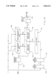
- FIGS. 1A and 1B are a block diagram of a video RAM according to the present invention.
- FIG. 2 is a block diagram illustrating one of the counters employed to implement the present invention.
- FIG. 3A is a schematic representation of VRAM memory
- FIG. 3B is a timing diagram illustrating the operation of the preferred embodiment of the present invention.
- a VRAM is an enhanced DRAM.
- the DRAM portion of a VRAM operates in a manner similar to known DRAM devices The DRAM portion is shown in FIG. 1A.
- Control signals RAS 105 and CAS 107 determine (via control logic 103) when to latch the address on the input pins into either the row address latch 104 or the column address latch 106.
- These latched addresses are decoded by column decoder 108 and row decoder 110 to point to one of the memory cells in the DRAM array 112. This cell is now selected to be read from or written to using, for example, the eight data Input/Output lines, D0-D7 114.
- FIG. 1B shows the additional circuitry that makes a DRAM into a VRAM.
- the major elements of this circuitry are the Low and High Data Registers 120, 122, also known as the Serial Access Memory registers ("SAM").
- SAM Serial Access Memory registers
- a 4 Mbit VRAM each 1024 element row is broken into two groups of 512 columns each. The selection of each group is done by the highest order bit of the latched column address 106.
- the SAM port is 512 columns wide and only connects to one group of columns at a time. (although 4 Mbit VRAMs are discussed, the invention is not constrained to any particularly density or organization of VRAM.)
- a Data Transfer is a special VRAM cycle that transfers data between a row in DRAM array 112 to the SAM registers 120, 122.
- the row address 104 is used to select which row to transfer. Since all the columns in a group will be transferred, the column address is not needed and is not latched. Instead the column address is latched into the SAM address latch 128 and is used as a starting address, or tap, for the SAM.
- the SAM is a sequential serial port so the addressing is generated by a counter.
- the SAM address latch is loaded into the SAM address counter 130 to set a starting address.
- Each subsequent Serial Clock cycle, SC 132 clocks the counter and points to the next register location (via SAM decoder 134) to supply data on the Serial data I/O lines, SD0-SD7 136.
- Second generation VRAMs have added another special cycle called a Split Data Transfer. This cycle breaks the 512 columns selected into two halves of 256 columns. Each half of 256 columns can be loaded into the SAM independent of the other half. Each half of the SAM also has its own tap address.
- Present VRAMs indicate which half of the SAM is actively being addressed by a status output QSF. Present VRAMs start at the tap address and continue incrementing until the boundary, e.g. at 255 or 511 is reached. At this point a new tap address is loaded from the SAM address latch and QSF switches (i.e. from high to low or vice versa).
- a number of SAM Address Counter 130 configurations can be used to generate the SAM addresses.
- One such method is to have two 8-bit counters that each generate 256 addresses.
- One of the counters generates even addresses from 0 to 510.
- the second counter generates odd addresses from 1 to 511.
- the selection of the odd or even counter to supply the address is done by the 9th bit of the SAM address latch.
- a counter of this type is shown in FIG. 2.
- the counter shown in FIG. 2 represents one of the two counters that would be used to generate the SAM addresses.
- the starting point or tap address from SAM address latch 128 is loaded into the counter to initialize the counter on lines 140.
- the counter is incremented by clock signal 142 generated by the control logic 103.
- Pre-decoders 144, 146, 148 and 150 each provide four bits to the next SAM address decode stage. While the preferred embodiment employs this form of dual counter, the present invention is in no way limited to implementation using this form of counter. For example, a single counter generating the full nine bit address could be employed as well.
- the preferred embodiment of the present invention proposes to replace the QSF status output with an input control pin, SRS 180, Split Register Select.
- the present invention seeks to replace a pin rather than adding a new control pin due to packaging limitations which limit the total number of input and output pins available.
- the invention could be equally well implemented by simply adding an extra SRS control pin.
- Control over jumping to the tap address in the other half of the SAM register is implemented by using the SRS to control the loading of the SAM address counter 130.
- Signal LDS 181 causes the counter to be loaded with the data on lines 140.
- the present invention thus provides a means to select a stopping or switching point in the SAM before the end of the half SAM boundary is reached.
- the SRS signal is OR'ed with control signal CNT0 182 that causes the switch at the end of one half of the SAM.
- the OR indicates that if SRS is kept inactive during VRAM cycles that do not use the SRS function the VRAM will function as a prior art VRAM normally would function.
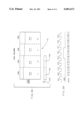
- FIGS. 3A-3B are respectively a conceptual representation of the architecture and a timing diagram that shows the use of SRS.
- FIG. 3A shows the DRAM array 112 and the SAM registers 120 and 122. The DRAM array has been divided into four segments 210, 212, 214 and 216.
- Clock signal 132 is shown entering the SAM section.
- FIG. 3B is a timing diagram. The pulses of serial clock 132 are shown at the top with the high value shown as SC1, SC2, etc.
- the value of SRS signal 180 is shown in the middle of the bottom portion.
- the bottom portions labelled "data" indicates the data being transferred out of serial access memory on lines 136. Following pulse SC1, data byte 1 from the lower portion of the SAM register (1L) is being transferred.
- serial clock 132 This is followed, for subsequent pulses of serial clock 132, by the transfer of data bytes 2L, 3L and 4L.
- SRS signal 180 changes from low to high value.
- SAM counter 130 This causes SAM counter 130 to be reloaded with a new tap address from SAM address latch 128 causing subsequent data to be output from the high data register 122.
- the data output is 1H, 2H, etc.
- the preferred embodiment does not require SRS signal 180 to maintain a high value.
- the jumping or reloading of the counter occurs based upon a change in the SRS signal from low to high value. Once the address loading has occurred, SRS may be returned to low value at any time. A shift from the high data register to the low data register could be caused by again bringing SRS 180 to a high value.
- data is selected as a portion of one row among the rows of the DRAM array for transfer to the serial access memory.
- the data may be selected as a portion of a column to be transferred to the serial access memory with the same effects as described above.
- the data has been described as a specific portion of one row or one column, but it may be divided into a larger or smaller number of portions than that described herein. For example, while the present invention loads 1/4 of one row into 1/2 of a serial access memory, in other embodiments, 1/2 of a row or 1/8 of a row may be loaded.
- an additional number of serial access registers could be employed instead of the two shown in the present embodiment. Thus more than two serial access memories may be provided with the same effects as described above.
Abstract
Description
Claims (11)
Priority Applications (4)
| Application Number | Priority Date | Filing Date | Title |
|---|---|---|---|
| US07/352,802 US5001672A (en) | 1989-05-16 | 1989-05-16 | Video ram with external select of active serial access register |
| DE69016094T DE69016094T2 (en) | 1989-05-16 | 1990-04-23 | Video random access memory. |
| EP90304326A EP0398511B1 (en) | 1989-05-16 | 1990-04-23 | Video random access memory |
| JP2123222A JPH0636311B2 (en) | 1989-05-16 | 1990-05-15 | Dual port VRAM memory |
Applications Claiming Priority (1)
| Application Number | Priority Date | Filing Date | Title |
|---|---|---|---|
| US07/352,802 US5001672A (en) | 1989-05-16 | 1989-05-16 | Video ram with external select of active serial access register |
Publications (1)
| Publication Number | Publication Date |
|---|---|
| US5001672A true US5001672A (en) | 1991-03-19 |
Family
ID=23386552
Family Applications (1)
| Application Number | Title | Priority Date | Filing Date |
|---|---|---|---|
| US07/352,802 Expired - Fee Related US5001672A (en) | 1989-05-16 | 1989-05-16 | Video ram with external select of active serial access register |
Country Status (4)
| Country | Link |
|---|---|
| US (1) | US5001672A (en) |
| EP (1) | EP0398511B1 (en) |
| JP (1) | JPH0636311B2 (en) |
| DE (1) | DE69016094T2 (en) |
Cited By (31)
| Publication number | Priority date | Publication date | Assignee | Title |
|---|---|---|---|---|
| US5179372A (en) * | 1990-06-19 | 1993-01-12 | International Business Machines Corporation | Video Random Access Memory serial port access |
| US5257237A (en) * | 1989-05-16 | 1993-10-26 | International Business Machines Corporation | SAM data selection on dual-ported DRAM devices |
| US5268682A (en) * | 1991-10-07 | 1993-12-07 | Industrial Technology Research Institute | Resolution independent raster display system |
| US5270973A (en) * | 1990-08-06 | 1993-12-14 | Texas Instruments Incorporated | Video random access memory having a split register and a multiplexer |
| US5287324A (en) * | 1991-03-29 | 1994-02-15 | Kabushiki Kaisha Toshiba | Multiport DRAM |
| US5289426A (en) * | 1990-06-11 | 1994-02-22 | Kabushiki Kaisha Toshiba | Dual port memory having address conversion function |
| US5321425A (en) * | 1992-02-19 | 1994-06-14 | Industrial Technology Research Institute | Resolution independent screen refresh strategy |
| US5367632A (en) * | 1992-10-30 | 1994-11-22 | International Business Machines Corporation | Flexible memory controller for graphics applications |
| US5394172A (en) * | 1993-03-11 | 1995-02-28 | Micron Semiconductor, Inc. | VRAM having isolated array sections for providing write functions that will not affect other array sections |
| US5422998A (en) * | 1993-11-15 | 1995-06-06 | Margolin; Jed | Video memory with flash fill |
| US5450367A (en) * | 1991-05-16 | 1995-09-12 | International Business Machines Corporation | Split SAM with independent SAM access |
| US5517609A (en) * | 1990-08-06 | 1996-05-14 | Texas Instruments Incorporated | Graphics display system using tiles of data |
| US5521877A (en) * | 1993-08-09 | 1996-05-28 | Nec Corporation | Serial random access memory device capable of reducing peak current through subword data register |
| US5581733A (en) * | 1990-03-13 | 1996-12-03 | Kabushiki Kaisha Toshiba | Data transfer control of a video memory having a multi-divisional random access memory and a multi-divisional serial access memory |
| US5748201A (en) * | 1994-03-16 | 1998-05-05 | Kabushiki Kaisha Toshiba | Semiconductor memory device having multiple modes that allow the cell array to be divided into a variable number of portions |
| US5815165A (en) * | 1990-01-10 | 1998-09-29 | Blixt; Stefan | Graphics processor |
| US5986913A (en) * | 1990-03-01 | 1999-11-16 | Texas Instruments Incorporated | Storage circuitry using sense amplifier shared between memories of differing number of rows |
| US6188635B1 (en) * | 1987-12-23 | 2001-02-13 | Texas Instruments Incorporated | Process of synchronously writing data to a dynamic random access memory array |
| US20020087790A1 (en) * | 1995-10-19 | 2002-07-04 | Barth Richard Maurice | Memory integrated circuit device which samples data upon detection of a strobe signal |
| US6493789B2 (en) | 1995-10-19 | 2002-12-10 | Rambus Inc. | Memory device which receives write masking and automatic precharge information |
| US6546446B2 (en) | 1990-04-18 | 2003-04-08 | Rambus Inc. | Synchronous memory device having automatic precharge |
| US6591353B1 (en) | 1995-10-19 | 2003-07-08 | Rambus Inc. | Protocol for communication with dynamic memory |
| US20040054845A1 (en) * | 2001-04-24 | 2004-03-18 | Rambus, Inc. | Method and apparatus for signaling between devices of a memory system |
| KR100481828B1 (en) * | 1997-05-19 | 2005-07-05 | 삼성전자주식회사 | Control method of memory using a variable address control circuit |
| US20050160241A1 (en) * | 1997-10-10 | 2005-07-21 | Rambus Inc. | High performance cost optimized memory |
| US6975292B1 (en) * | 1999-01-19 | 2005-12-13 | Fuji Photo Film Co., Ltd | Image display apparatus for photographing an object and displaying the photographed image |
| US20060039213A1 (en) * | 1990-04-18 | 2006-02-23 | Rambus Inc. | Integrated circuit I/O using a high performance bus interface |
| US20060077731A1 (en) * | 2001-04-24 | 2006-04-13 | Ware Frederick A | Memory module with termination component |
| US20060291587A1 (en) * | 1997-06-20 | 2006-12-28 | Massachusetts Institute Of Technology | Digital transmitter |
| US20070177436A1 (en) * | 1997-10-10 | 2007-08-02 | Davis Paul G | Memory System and Method for Two Step Memory Write Operations |
| US20070206429A1 (en) * | 2004-09-15 | 2007-09-06 | Ware Frederick A | Memory component with multiple delayed timing signals |
Families Citing this family (2)
| Publication number | Priority date | Publication date | Assignee | Title |
|---|---|---|---|---|
| JPH06102842A (en) * | 1990-08-06 | 1994-04-15 | Texas Instr Inc <Ti> | Graphic display system including video random access memory having divided serial register and operation counter |
| JPH0683316A (en) * | 1990-08-31 | 1994-03-25 | Texas Instr Inc <Ti> | Image display device and video ram chip |
Citations (2)
| Publication number | Priority date | Publication date | Assignee | Title |
|---|---|---|---|---|
| US4825411A (en) * | 1986-06-24 | 1989-04-25 | Mitsubishi Denki Kabushiki Kaisha | Dual-port memory with asynchronous control of serial data memory transfer |
| US4855959A (en) * | 1986-07-04 | 1989-08-08 | Nec Corporation | Dual port memory circuit |
-
1989
- 1989-05-16 US US07/352,802 patent/US5001672A/en not_active Expired - Fee Related
-
1990
- 1990-04-23 EP EP90304326A patent/EP0398511B1/en not_active Expired - Lifetime
- 1990-04-23 DE DE69016094T patent/DE69016094T2/en not_active Expired - Fee Related
- 1990-05-15 JP JP2123222A patent/JPH0636311B2/en not_active Expired - Lifetime
Patent Citations (2)
| Publication number | Priority date | Publication date | Assignee | Title |
|---|---|---|---|---|
| US4825411A (en) * | 1986-06-24 | 1989-04-25 | Mitsubishi Denki Kabushiki Kaisha | Dual-port memory with asynchronous control of serial data memory transfer |
| US4855959A (en) * | 1986-07-04 | 1989-08-08 | Nec Corporation | Dual port memory circuit |
Cited By (130)
| Publication number | Priority date | Publication date | Assignee | Title |
|---|---|---|---|---|
| US6188635B1 (en) * | 1987-12-23 | 2001-02-13 | Texas Instruments Incorporated | Process of synchronously writing data to a dynamic random access memory array |
| US5257237A (en) * | 1989-05-16 | 1993-10-26 | International Business Machines Corporation | SAM data selection on dual-ported DRAM devices |
| US5815165A (en) * | 1990-01-10 | 1998-09-29 | Blixt; Stefan | Graphics processor |
| US5986913A (en) * | 1990-03-01 | 1999-11-16 | Texas Instruments Incorporated | Storage circuitry using sense amplifier shared between memories of differing number of rows |
| US6134637A (en) * | 1990-03-13 | 2000-10-17 | Kabushiki Kaisha Toshiba | Data transfer control of a video memory having a multi-divisional random access memory and a multi-divisional serial access memory |
| US5893167A (en) * | 1990-03-13 | 1999-04-06 | Toda; Haruki | Data transfer control of a video memory having a multi-divisional random access memory and a multi-divisional serial access |
| US6389521B1 (en) | 1990-03-13 | 2002-05-14 | Kabushiki Kaisha Toshiba | Data transfer control of a video memory having a multi-divisional random access memory and a multi-divisional serial access memory |
| US5581733A (en) * | 1990-03-13 | 1996-12-03 | Kabushiki Kaisha Toshiba | Data transfer control of a video memory having a multi-divisional random access memory and a multi-divisional serial access memory |
| US6546446B2 (en) | 1990-04-18 | 2003-04-08 | Rambus Inc. | Synchronous memory device having automatic precharge |
| US20060039213A1 (en) * | 1990-04-18 | 2006-02-23 | Rambus Inc. | Integrated circuit I/O using a high performance bus interface |
| US20050030802A1 (en) * | 1990-04-18 | 2005-02-10 | Rambus Inc. | Memory module including an integrated circuit device |
| US6564281B2 (en) | 1990-04-18 | 2003-05-13 | Rambus Inc. | Synchronous memory device having automatic precharge |
| US20050033903A1 (en) * | 1990-04-18 | 2005-02-10 | Rambus Inc. | Integrated circuit device |
| US5289426A (en) * | 1990-06-11 | 1994-02-22 | Kabushiki Kaisha Toshiba | Dual port memory having address conversion function |
| US5179372A (en) * | 1990-06-19 | 1993-01-12 | International Business Machines Corporation | Video Random Access Memory serial port access |
| US5517609A (en) * | 1990-08-06 | 1996-05-14 | Texas Instruments Incorporated | Graphics display system using tiles of data |
| US5270973A (en) * | 1990-08-06 | 1993-12-14 | Texas Instruments Incorporated | Video random access memory having a split register and a multiplexer |
| US5287324A (en) * | 1991-03-29 | 1994-02-15 | Kabushiki Kaisha Toshiba | Multiport DRAM |
| US5450367A (en) * | 1991-05-16 | 1995-09-12 | International Business Machines Corporation | Split SAM with independent SAM access |
| US5268682A (en) * | 1991-10-07 | 1993-12-07 | Industrial Technology Research Institute | Resolution independent raster display system |
| US5321425A (en) * | 1992-02-19 | 1994-06-14 | Industrial Technology Research Institute | Resolution independent screen refresh strategy |
| US5367632A (en) * | 1992-10-30 | 1994-11-22 | International Business Machines Corporation | Flexible memory controller for graphics applications |
| US5594474A (en) * | 1993-03-11 | 1997-01-14 | Micron Technology, Inc. | VRAM having isolated array sections for providing write functions that will not affect other array sections |
| US5394172A (en) * | 1993-03-11 | 1995-02-28 | Micron Semiconductor, Inc. | VRAM having isolated array sections for providing write functions that will not affect other array sections |
| US5521877A (en) * | 1993-08-09 | 1996-05-28 | Nec Corporation | Serial random access memory device capable of reducing peak current through subword data register |
| US5553229A (en) * | 1993-11-15 | 1996-09-03 | Margolin; Jed | Row addressable graphics memory with flash fill |
| US5422998A (en) * | 1993-11-15 | 1995-06-06 | Margolin; Jed | Video memory with flash fill |
| US5890197A (en) * | 1994-03-16 | 1999-03-30 | Kabushiki Kaisha Toshiba | Semiconductor memory device having split transfer function |
| US5748201A (en) * | 1994-03-16 | 1998-05-05 | Kabushiki Kaisha Toshiba | Semiconductor memory device having multiple modes that allow the cell array to be divided into a variable number of portions |
| US6496897B2 (en) | 1995-10-19 | 2002-12-17 | Rambus Inc. | Semiconductor memory device which receives write masking information |
| US6493789B2 (en) | 1995-10-19 | 2002-12-10 | Rambus Inc. | Memory device which receives write masking and automatic precharge information |
| US6591353B1 (en) | 1995-10-19 | 2003-07-08 | Rambus Inc. | Protocol for communication with dynamic memory |
| US6681288B2 (en) | 1995-10-19 | 2004-01-20 | Rambus Inc. | Memory device with receives write masking information |
| US6470405B2 (en) | 1995-10-19 | 2002-10-22 | Rambus Inc. | Protocol for communication with dynamic memory |
| US20020087790A1 (en) * | 1995-10-19 | 2002-07-04 | Barth Richard Maurice | Memory integrated circuit device which samples data upon detection of a strobe signal |
| US6810449B1 (en) | 1995-10-19 | 2004-10-26 | Rambus, Inc. | Protocol for communication with dynamic memory |
| US6931467B2 (en) | 1995-10-19 | 2005-08-16 | Rambus Inc. | Memory integrated circuit device which samples data upon detection of a strobe signal |
| KR100481828B1 (en) * | 1997-05-19 | 2005-07-05 | 삼성전자주식회사 | Control method of memory using a variable address control circuit |
| US9419824B2 (en) | 1997-06-20 | 2016-08-16 | Massachusetts Institute Of Technology | Digital transmitter |
| US8243847B2 (en) | 1997-06-20 | 2012-08-14 | Massachusetts Institute Of Technology | Digital transmitter |
| US20090262794A1 (en) * | 1997-06-20 | 2009-10-22 | Massachusetts Institute Of Technology | Digital transmitter |
| US20110051794A1 (en) * | 1997-06-20 | 2011-03-03 | Massachusetts Institute Of Technology | Digital Transmitter |
| US8989303B2 (en) | 1997-06-20 | 2015-03-24 | Massachusetts Institute Of Technology | Digital transmitter |
| US9647857B2 (en) | 1997-06-20 | 2017-05-09 | Massachusetts Institute Of Technology | Digital transmitter |
| US8923433B2 (en) | 1997-06-20 | 2014-12-30 | Massachusetts Institute Of Technology | Digital transmitter |
| US8761235B2 (en) | 1997-06-20 | 2014-06-24 | Massachusetts Institute Of Technology | Digital transmitter |
| US8681837B2 (en) | 1997-06-20 | 2014-03-25 | Massachusetts Institute Of Technology | Digital Transmitter |
| US8238470B2 (en) | 1997-06-20 | 2012-08-07 | Massachusetts Institute Of Technology | Digital transmitter |
| US20060291587A1 (en) * | 1997-06-20 | 2006-12-28 | Massachusetts Institute Of Technology | Digital transmitter |
| US20100034252A1 (en) * | 1997-06-20 | 2010-02-11 | Dally William J | Digital Transmitter |
| US8238467B2 (en) | 1997-06-20 | 2012-08-07 | Massachusetts Institute Of Technology | Digital transmitter |
| US8311147B2 (en) | 1997-06-20 | 2012-11-13 | Massachusetts Institute Of Technology | Digital transmitter |
| US8259841B2 (en) | 1997-06-20 | 2012-09-04 | Massachusetts Institute Of Technology | Digital transmitter |
| US8254491B2 (en) | 1997-06-20 | 2012-08-28 | Massachusetts Institute Of Technology | Digital transmitter |
| US20070159912A1 (en) * | 1997-10-10 | 2007-07-12 | Barth Richard M | Integrated Circuit Memory Device with Delayed Write Command Processing |
| US8019958B2 (en) | 1997-10-10 | 2011-09-13 | Rambus Inc. | Memory write signaling and methods thereof |
| US20070147143A1 (en) * | 1997-10-10 | 2007-06-28 | Barth Richard M | Integrated Circuit Memory Device Having Delayed Write Capability |
| US8504790B2 (en) | 1997-10-10 | 2013-08-06 | Rambus Inc. | Memory component having write operation with multiple time periods |
| US20070177436A1 (en) * | 1997-10-10 | 2007-08-02 | Davis Paul G | Memory System and Method for Two Step Memory Write Operations |
| US20070198868A1 (en) * | 1997-10-10 | 2007-08-23 | Barth Richard M | Memory System Having Delayed Write Timing |
| US8560797B2 (en) | 1997-10-10 | 2013-10-15 | Rambus Inc. | Method and apparatus for indicating mask information |
| US20070242532A1 (en) * | 1997-10-10 | 2007-10-18 | Barth Richard M | Integrated Circuit Memory Device Having Delayed Write Timing Based on Read Response Time |
| US7287119B2 (en) | 1997-10-10 | 2007-10-23 | Rambus Inc. | Integrated circuit memory device with delayed write command processing |
| US8205056B2 (en) | 1997-10-10 | 2012-06-19 | Rambus Inc. | Memory controller for controlling write signaling |
| US8140805B2 (en) | 1997-10-10 | 2012-03-20 | Rambus Inc. | Memory component having write operation with multiple time periods |
| US7197611B2 (en) | 1997-10-10 | 2007-03-27 | Rambus Inc. | Integrated circuit memory device having write latency function |
| US7330952B2 (en) | 1997-10-10 | 2008-02-12 | Rambus Inc. | Integrated circuit memory device having delayed write timing based on read response time |
| US7330953B2 (en) | 1997-10-10 | 2008-02-12 | Rambus Inc. | Memory system having delayed write timing |
| US7360050B2 (en) | 1997-10-10 | 2008-04-15 | Rambus Inc. | Integrated circuit memory device having delayed write capability |
| US20080091907A1 (en) * | 1997-10-10 | 2008-04-17 | Barth Richard M | Integrated circuit memory device having delayed write timing based on read response time |
| US7437527B2 (en) | 1997-10-10 | 2008-10-14 | Rambus Inc. | Memory device with delayed issuance of internal write command |
| US20050160241A1 (en) * | 1997-10-10 | 2005-07-21 | Rambus Inc. | High performance cost optimized memory |
| US7870357B2 (en) | 1997-10-10 | 2011-01-11 | Rambus Inc. | Memory system and method for two step memory write operations |
| US20090031093A1 (en) * | 1997-10-10 | 2009-01-29 | Davis Paul G | Memory System and Method for Two Step Memory Write Operations |
| US7496709B2 (en) | 1997-10-10 | 2009-02-24 | Rambus Inc. | Integrated circuit memory device having delayed write timing based on read response time |
| US20100332719A1 (en) * | 1997-10-10 | 2010-12-30 | Barth Richard M | Memory Write Signaling and Methods Thereof |
| US7793039B2 (en) | 1997-10-10 | 2010-09-07 | Rambus Inc. | Interface for a semiconductor memory device and method for controlling the interface |
| US6975292B1 (en) * | 1999-01-19 | 2005-12-13 | Fuji Photo Film Co., Ltd | Image display apparatus for photographing an object and displaying the photographed image |
| US20040054845A1 (en) * | 2001-04-24 | 2004-03-18 | Rambus, Inc. | Method and apparatus for signaling between devices of a memory system |
| US9053778B2 (en) | 2001-04-24 | 2015-06-09 | Rambus Inc. | Memory controller that enforces strobe-to-strobe timing offset |
| US10706910B2 (en) | 2001-04-24 | 2020-07-07 | Rambus Inc. | Memory controller |
| US10236051B2 (en) | 2001-04-24 | 2019-03-19 | Rambus Inc. | Memory controller |
| US20090063887A1 (en) * | 2001-04-24 | 2009-03-05 | Ware Frederick A | Memory module with termination component |
| US7484064B2 (en) | 2001-04-24 | 2009-01-27 | Rambus Inc. | Method and apparatus for signaling between devices of a memory system |
| US9741424B2 (en) | 2001-04-24 | 2017-08-22 | Rambus Inc. | Memory controller |
| US20040170072A1 (en) * | 2001-04-24 | 2004-09-02 | Rambus Inc. | Method and apparatus for coordinating memory operations among diversely-located memory components |
| US9472262B2 (en) | 2001-04-24 | 2016-10-18 | Rambus Inc. | Memory controller |
| US20070255919A1 (en) * | 2001-04-24 | 2007-11-01 | Ware Frederick A | Memory controller device having timing offset capability |
| US20070247935A1 (en) * | 2001-04-24 | 2007-10-25 | Ware Frederick A | Clocked Memory System with Termination Component |
| US8214616B2 (en) | 2001-04-24 | 2012-07-03 | Rambus Inc. | Memory controller device having timing offset capability |
| US20050169097A1 (en) * | 2001-04-24 | 2005-08-04 | Rambus Inc. | Method and apparatus for coordinating memory operations among diversely-located memory components |
| US9311976B2 (en) | 2001-04-24 | 2016-04-12 | Rambus Inc. | Memory module |
| US7225292B2 (en) | 2001-04-24 | 2007-05-29 | Rambus Inc. | Memory module with termination component |
| US7225311B2 (en) | 2001-04-24 | 2007-05-29 | Rambus Inc. | Method and apparatus for coordinating memory operations among diversely-located memory components |
| US7210016B2 (en) | 2001-04-24 | 2007-04-24 | Rambus Inc. | Method, system and memory controller utilizing adjustable write data delay settings |
| US7209397B2 (en) | 2001-04-24 | 2007-04-24 | Rambus Inc. | Memory device with clock multiplier circuit |
| US7200055B2 (en) | 2001-04-24 | 2007-04-03 | Rambus Inc. | Memory module with termination component |
| US8320202B2 (en) | 2001-04-24 | 2012-11-27 | Rambus Inc. | Clocked memory system with termination component |
| US8359445B2 (en) | 2001-04-24 | 2013-01-22 | Rambus Inc. | Method and apparatus for signaling between devices of a memory system |
| US20060007761A1 (en) * | 2001-04-24 | 2006-01-12 | Ware Frederick A | Memory module with termination component |
| US8391039B2 (en) | 2001-04-24 | 2013-03-05 | Rambus Inc. | Memory module with termination component |
| US8395951B2 (en) | 2001-04-24 | 2013-03-12 | Rambus Inc. | Memory controller |
| US8462566B2 (en) | 2001-04-24 | 2013-06-11 | Rambus Inc. | Memory module with termination component |
| US20060039174A1 (en) * | 2001-04-24 | 2006-02-23 | Ware Frederick A | Memory module with termination component |
| US7177998B2 (en) | 2001-04-24 | 2007-02-13 | Rambus Inc. | Method, system and memory controller utilizing adjustable read data delay settings |
| US8537601B2 (en) | 2001-04-24 | 2013-09-17 | Rambus Inc. | Memory controller with selective data transmission delay |
| US20060129776A1 (en) * | 2001-04-24 | 2006-06-15 | Ware Frederick A | Method, system and memory controller utilizing adjustable read data delay settings |
| US8625371B2 (en) | 2001-04-24 | 2014-01-07 | Rambus Inc. | Memory component with terminated and unterminated signaling inputs |
| US20060077731A1 (en) * | 2001-04-24 | 2006-04-13 | Ware Frederick A | Memory module with termination component |
| US8717837B2 (en) | 2001-04-24 | 2014-05-06 | Rambus Inc. | Memory module |
| US8760944B2 (en) | 2001-04-24 | 2014-06-24 | Rambus Inc. | Memory component that samples command/address signals in response to both edges of a clock signal |
| US20060069895A1 (en) * | 2001-04-24 | 2006-03-30 | Ware Frederick A | Method, system and memory controller utilizing adjustable write data delay settings |
| US8743636B2 (en) | 2004-09-15 | 2014-06-03 | Rambus Inc. | Memory module having a write-timing calibration mode |
| US8493802B1 (en) | 2004-09-15 | 2013-07-23 | Rambus Inc. | Memory controller having a write-timing calibration mode |
| US8363493B2 (en) | 2004-09-15 | 2013-01-29 | Rambus Inc. | Memory controller having a write-timing calibration mode |
| US7724590B2 (en) | 2004-09-15 | 2010-05-25 | Rambus Inc. | Memory controller with multiple delayed timing signals |
| US9229470B2 (en) | 2004-09-15 | 2016-01-05 | Rambus Inc. | Memory controller with clock-to-strobe skew compensation |
| US20070206429A1 (en) * | 2004-09-15 | 2007-09-06 | Ware Frederick A | Memory component with multiple delayed timing signals |
| US8218382B2 (en) | 2004-09-15 | 2012-07-10 | Rambus Inc. | Memory component having a write-timing calibration mode |
| US9437279B2 (en) | 2004-09-15 | 2016-09-06 | Rambus Inc. | Memory controller with clock-to-strobe skew compensation |
| US8045407B2 (en) | 2004-09-15 | 2011-10-25 | Rambus Inc. | Memory-write timing calibration including generation of multiple delayed timing signals |
| US7301831B2 (en) | 2004-09-15 | 2007-11-27 | Rambus Inc. | Memory systems with variable delays for write data signals |
| US7480193B2 (en) | 2004-09-15 | 2009-01-20 | Rambus Inc. | Memory component with multiple delayed timing signals |
| US9830971B2 (en) | 2004-09-15 | 2017-11-28 | Rambus Inc. | Memory controller with clock-to-strobe skew compensation |
| US20090063890A1 (en) * | 2004-09-15 | 2009-03-05 | Ware Frederick A | Memory controller with multiple delayed timing signals |
| US10325645B2 (en) | 2004-09-15 | 2019-06-18 | Rambus Inc. | Memory controller with clock-to-strobe skew compensation |
| US20100188911A1 (en) * | 2004-09-15 | 2010-07-29 | Ware Frederick A | Memory-write timing calibration including generation of multiple delayed timing signals |
| US10755764B2 (en) | 2004-09-15 | 2020-08-25 | Rambus Inc. | Memory component that enables calibrated command- and data-timing signal arrival |
| US11100976B2 (en) | 2004-09-15 | 2021-08-24 | Rambus Inc. | Memory controller with clock-to-strobe skew compensation |
| US11664067B2 (en) | 2004-09-15 | 2023-05-30 | Rambus Inc. | Memory system component that enables clock-to-strobe skew compensation |
Also Published As
| Publication number | Publication date |
|---|---|
| JPH0636311B2 (en) | 1994-05-11 |
| JPH035991A (en) | 1991-01-11 |
| EP0398511A2 (en) | 1990-11-22 |
| DE69016094D1 (en) | 1995-03-02 |
| EP0398511A3 (en) | 1992-04-01 |
| EP0398511B1 (en) | 1995-01-18 |
| DE69016094T2 (en) | 1995-06-29 |
Similar Documents
| Publication | Publication Date | Title |
|---|---|---|
| US5001672A (en) | Video ram with external select of active serial access register | |
| EP0398510B1 (en) | Video random access memory | |
| US4807189A (en) | Read/write memory having a multiple column select mode | |
| US4646270A (en) | Video graphic dynamic RAM | |
| US5195056A (en) | Read/write memory having an on-chip input data register, having pointer circuits between a serial data register and input/output buffer circuits | |
| US4817058A (en) | Multiple input/output read/write memory having a multiple-cycle write mask | |
| EP0197413B1 (en) | Frame buffer memory | |
| US5148524A (en) | Dynamic video RAM incorporating on chip vector/image mode line modification | |
| EP0176801B1 (en) | A peripheral apparatus for image memories | |
| US5142637A (en) | Dynamic video RAM incorporating single clock random port control | |
| US5148523A (en) | Dynamic video RAM incorporationg on chip line modification | |
| KR940006362B1 (en) | Semiconductor memory device | |
| US4870621A (en) | Dual port memory device with improved serial access scheme | |
| JP2593060B2 (en) | Dynamic random access memory, dynamic random access memory access method and system | |
| US5257237A (en) | SAM data selection on dual-ported DRAM devices | |
| JPS61288240A (en) | Semiconductor storage device | |
| US5991186A (en) | Four-bit block write for a wide input/output random access memory in a data processing system | |
| JP3550510B2 (en) | Dynamic random access memory device, data transfer system and data writing method | |
| US5097256A (en) | Method of generating a cursor | |
| JP3179792B2 (en) | Multi-port random access memory | |
| KR950004743B1 (en) | Multi-port random access memory and access method | |
| EP0474435A2 (en) | A graphics display system with a video random access memory having a one-half row length register for serial access to the memory | |
| JPH04195440A (en) | Semiconductor memory suitable for frame buffer and graphic processor using the same |
Legal Events
| Date | Code | Title | Description |
|---|---|---|---|
| AS | Assignment |
Owner name: INTERNATIONAL BUSINESS MACHINES CORPORATION, ARMON Free format text: ASSIGNMENT OF ASSIGNORS INTEREST.;ASSIGNORS:EBBERS, TIMOTHY J.;GUPTA, SATISH;HENDERSON, RANDALL L.;AND OTHERS;REEL/FRAME:005500/0008;SIGNING DATES FROM 19890629 TO 19890712 Owner name: INTERNATIONAL BUSINESS MACHINES CORPORATION, NEW Y Free format text: ASSIGNMENT OF ASSIGNORS INTEREST.;ASSIGNORS:EBBERS, TIMOTHY J.;GUPTA, SATISH;HENDERSON, RANDALL L.;AND OTHERS;REEL/FRAME:006073/0003;SIGNING DATES FROM 19890629 TO 19890712 |
|
| REFU | Refund |
Free format text: REFUND OF EXCESS PAYMENTS PROCESSED (ORIGINAL EVENT CODE: R169); ENTITY STATUS OF PATENT OWNER: LARGE ENTITY |
|
| FPAY | Fee payment |
Year of fee payment: 4 |
|
| FEPP | Fee payment procedure |
Free format text: PAYOR NUMBER ASSIGNED (ORIGINAL EVENT CODE: ASPN); ENTITY STATUS OF PATENT OWNER: LARGE ENTITY |
|
| FPAY | Fee payment |
Year of fee payment: 8 |
|
| FEPP | Fee payment procedure |
Free format text: PAYOR NUMBER ASSIGNED (ORIGINAL EVENT CODE: ASPN); ENTITY STATUS OF PATENT OWNER: LARGE ENTITY Free format text: PAYER NUMBER DE-ASSIGNED (ORIGINAL EVENT CODE: RMPN); ENTITY STATUS OF PATENT OWNER: LARGE ENTITY |
|
| REMI | Maintenance fee reminder mailed | ||
| LAPS | Lapse for failure to pay maintenance fees | ||
| STCH | Information on status: patent discontinuation |
Free format text: PATENT EXPIRED DUE TO NONPAYMENT OF MAINTENANCE FEES UNDER 37 CFR 1.362 |
|
| FP | Lapsed due to failure to pay maintenance fee |
Effective date: 20030319 |