US4997790A - Process for forming a self-aligned contact structure - Google Patents
Process for forming a self-aligned contact structure Download PDFInfo
- Publication number
- US4997790A US4997790A US07/566,185 US56618590A US4997790A US 4997790 A US4997790 A US 4997790A US 56618590 A US56618590 A US 56618590A US 4997790 A US4997790 A US 4997790A
- Authority
- US
- United States
- Prior art keywords
- insulating layer
- film
- depositing
- layer
- conductive members
- Prior art date
- Legal status (The legal status is an assumption and is not a legal conclusion. Google has not performed a legal analysis and makes no representation as to the accuracy of the status listed.)
- Expired - Lifetime
Links
Images


Classifications
-
- H—ELECTRICITY
- H01—ELECTRIC ELEMENTS
- H01L—SEMICONDUCTOR DEVICES NOT COVERED BY CLASS H10
- H01L21/00—Processes or apparatus adapted for the manufacture or treatment of semiconductor or solid state devices or of parts thereof
- H01L21/70—Manufacture or treatment of devices consisting of a plurality of solid state components formed in or on a common substrate or of parts thereof; Manufacture of integrated circuit devices or of parts thereof
- H01L21/71—Manufacture of specific parts of devices defined in group H01L21/70
- H01L21/768—Applying interconnections to be used for carrying current between separate components within a device comprising conductors and dielectrics
- H01L21/76897—Formation of self-aligned vias or contact plugs, i.e. involving a lithographically uncritical step
-
- H—ELECTRICITY
- H01—ELECTRIC ELEMENTS
- H01L—SEMICONDUCTOR DEVICES NOT COVERED BY CLASS H10
- H01L21/00—Processes or apparatus adapted for the manufacture or treatment of semiconductor or solid state devices or of parts thereof
- H01L21/70—Manufacture or treatment of devices consisting of a plurality of solid state components formed in or on a common substrate or of parts thereof; Manufacture of integrated circuit devices or of parts thereof
- H01L21/71—Manufacture of specific parts of devices defined in group H01L21/70
- H01L21/768—Applying interconnections to be used for carrying current between separate components within a device comprising conductors and dielectrics
- H01L21/76838—Applying interconnections to be used for carrying current between separate components within a device comprising conductors and dielectrics characterised by the formation and the after-treatment of the conductors
- H01L21/76885—By forming conductive members before deposition of protective insulating material, e.g. pillars, studs
-
- H—ELECTRICITY
- H01—ELECTRIC ELEMENTS
- H01L—SEMICONDUCTOR DEVICES NOT COVERED BY CLASS H10
- H01L24/00—Arrangements for connecting or disconnecting semiconductor or solid-state bodies; Methods or apparatus related thereto
- H01L24/01—Means for bonding being attached to, or being formed on, the surface to be connected, e.g. chip-to-package, die-attach, "first-level" interconnects; Manufacturing methods related thereto
- H01L24/10—Bump connectors ; Manufacturing methods related thereto
- H01L24/11—Manufacturing methods
-
- Y—GENERAL TAGGING OF NEW TECHNOLOGICAL DEVELOPMENTS; GENERAL TAGGING OF CROSS-SECTIONAL TECHNOLOGIES SPANNING OVER SEVERAL SECTIONS OF THE IPC; TECHNICAL SUBJECTS COVERED BY FORMER USPC CROSS-REFERENCE ART COLLECTIONS [XRACs] AND DIGESTS
- Y10—TECHNICAL SUBJECTS COVERED BY FORMER USPC
- Y10S—TECHNICAL SUBJECTS COVERED BY FORMER USPC CROSS-REFERENCE ART COLLECTIONS [XRACs] AND DIGESTS
- Y10S148/00—Metal treatment
- Y10S148/105—Masks, metal
-
- Y—GENERAL TAGGING OF NEW TECHNOLOGICAL DEVELOPMENTS; GENERAL TAGGING OF CROSS-SECTIONAL TECHNOLOGIES SPANNING OVER SEVERAL SECTIONS OF THE IPC; TECHNICAL SUBJECTS COVERED BY FORMER USPC CROSS-REFERENCE ART COLLECTIONS [XRACs] AND DIGESTS
- Y10—TECHNICAL SUBJECTS COVERED BY FORMER USPC
- Y10S—TECHNICAL SUBJECTS COVERED BY FORMER USPC CROSS-REFERENCE ART COLLECTIONS [XRACs] AND DIGESTS
- Y10S148/00—Metal treatment
- Y10S148/161—Tapered edges
Definitions
- This invention relates to semiconductor fabrication processes in general, and more specifically to a process for forming contacts in multi-layer semiconductor devices.
- Another common semiconductor device fabrication problem is the guaranteeing of electrical isolation of a self-aligned contact from underlying conductive members. While etching an insulating layer of the device, sidewall spacers are often formed along conductive members to provide electrical isolation. However, in order to completely etch the insulating material from an area in which a contact is to be formed, the integrity of the sidewall spacers is typically difficult to maintain during the etch process. Sidewall spacers are also attacked during subsequent cleaning steps. Without adequate isolation, the conductive members may be electrically shorted to other conductive members, for instance a contact, possibly causing the device to fail.
- a first insulating layer is provided, overlying a substrate material.
- a film of material is deposited overlying the first insulating layer, the film of material having the ability to be etched selectively to the first insulating layer.
- the film of material is selectively etched to expose areas of the first insulating layer, and a second insulating layer is deposited overlying the exposed areas of the first insulating layer and the film of material.
- the second insulating layer is etched to expose the film of material.
- the film of material is selectively etched to expose areas of the first insulating layer, while keeping the first and second insulating layers substantially unaltered. Selected areas of the substrate material are exposed by anisotropically etching the exposed areas of the first insulating layer. A conductive layer is deposited and patterned, thereby forming a contact to the exposed areas of the substrate material.
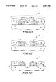
- FIGS. 1A-1G are cross-sectional views of a semiconductor device fabrication process in which a self-aligned contact structure is formed in accordance with the present invention.
- FIGS. 2A-2G are cross-sectional views illustrating another embodiment of the present invention.
- FIGS. 1A-1G represent one form of the invention in which the problems noted above are resolved.
- a semiconductor device 10 includes spaced apart conductive members 14 overlying a substrate material 12.
- Conductive members 14 are typically of the same material, generally comprising one of polysilicon, aluminum, aluminum alloys, tungsten, or other conductive materials.
- the distance between conductive members 14 is assumed to be in the sub-micron to two microns range but may be extended outside this range.
- Substrate material 12 is typically made of silicon, but may be of another material, such as any of the III-V compounds used in the semiconductor industry. It should be noted that substrate material 12 may also be an intermediate layer of a semiconductor device such as a polysilicon or metal layer, rather than the bulk of a semiconductor device.
- a dielectric layer 15 is patterned on conductive members 14 for reasons to be discussed later. Dielectric layer 15 may be one of or a combination of SiO 2 , Si 3 N 4 , or any other material which may be used as a dielectric.
- a first insulating layer 16 is deposited onto device 10 in FIG. 1A. Insulating materials such as SiO 2 , PSG (phospho-silicate-glass), or BPSG (boron doped phospho-silicate-glass) are commonly used materials which are suitable for first insulating layer 16.
- FIG. 1B illustrates the process by which a sacrificial plug is formed to define a contact opening.
- a film of material 18 is deposited onto device 10.
- the composition of film of material 18 is chosen such that the film of material 18 can be selectively etched with respect to insulating materials used in fabricating device 10.
- polysilicon and Si 3 N 4 are each suitable for film of material 18 since they can be etched selective to most insulating oxide layers.
- Tungsten or titanium nitride may also be used for film of material 18.
- the thickness of film of material 18 may depend on other requirements if film of material 18 is also incorporated into actual circuitry on other portions of semiconductor device 10.
- a photoresist layer is deposited and patterned to form a photoresist mask 20, using conventional photolithography techniques.
- the photoresist layer is patterned such that the area in which a contact is to be formed is defined as the area underlying photoresist mask 20.
- the unmasked portions of the film of material 18 are removed by exposing device 10 to an etch, thereby forming a sacrificial plug 22, as illustrated in FIG. 1C.
- the etching of film of material 18 to form sacrificial plug 22 may be accomplished by using either wet or dry etch chemistries, depending on the choice of material for film of material 18. For example, a wet etch chemistry of nitric and HF (hydrofluoric) acids will remove a polysilicon film without damaging an underlying oxide layer. Likewise, a heated phosphoric acid could be used to remove a Si 3 N 4 film while maintaining the integrity of an underlying oxide layer. Dry etching using chlorine-based chemistries will also provide the same result of forming a sacrificial plug 22, while not substantially attacking the underlying first insulating layer 16.
- Second insulating layer 24 is deposited onto device 10.
- Second insulating layer 24 may be comprised of materials such as those suitable for first insulating layer 16, including, but not limited to SiO 2 , PSG, or BPSG. Possible deposition techniques for these insulating materials are CVD (chemical vapor deposition) using SiH 4 or TEOS (tetra-ethyl-ortho-silicate) source gases or using a SOG (spin-on-glass).
- CVD chemical vapor deposition
- TEOS tetra-ethyl-ortho-silicate
- SOG spin-on-glass
- the planarization of the device may be achieved in a variety of ways.
- the second insulating layer 24 may be deposited thickly, on the order of 0.5-1.5 ⁇ m, and then etched back to provide a planarized layer.
- Another planarization technique is to deposit the second insulating layer 24 as illustrated by curved line 1--1 and heat the device 10, thereby flowing the second insulating layer. If using SOG as the second insulating layer 24, the device becomes planar upon deposition. Once the second insulating layer 24 is deposited and device 10 is planarized, the device is subjected to a blanket etch which uniformly etches a top portion of the second insulating layer 24 from device 10.
- the etch is stopped at the point in which the sacrificial plug 22 is exposed, as illustrated in FIG. 1D.
- the material of sacrificial plug 22 may be chosen so that the material provides for a good etch-stop as well. For instance, a polysilicon sacrificial plug will provide a good etch-stop for most insulating oxide layers since the selectivity of an oxide etch to polysilicon is quite high. Either a timed etch or an etch having endpoint detection capability would be suitable for use in exposing sacrificial plug 22.
- the exposed sacrificial plug 22 is removed, as in FIG. 1E, using an etch which is selective to the material chosen for the first and second insulating layers, 16 and 24 respectively.
- the desired result is to remove sacrificial plug 22 without substantially altering the first and second insulating layers, 16 and 24 respectively.
- a wet etch chemistry of nitric and HF (hydrofluoric) acids will remove the sacrificial plug without damaging any surrounding oxide regions.
- a heated phosphoric acid could be used to remove a Si 3 N 4 sacrificial plug while maintaining the integrity of oxide regions such as dielectric layer 15. Dry etching may also be used to remove sacrificial plug 22.
- Selective planarization is an improvement over existing planarization techniques in that selective planarization reduces the need to etch through thick insulating layers to form vias or contact openings.
- first insulating layer 16 and gate oxide layer 13 In order to make electrical contact to substrate material 12, portions of first insulating layer 16 and gate oxide layer 13 must be removed. As illustrated in FIG. 1F, device 10 is subjected to an anisotropic etch to expose a portion of the underlying substrate material 12 while keeping conductive members 14 isolated by maintaining an insulating material on all sides.
- An anisotropic etch of first insulating layer 16 forms sidewall spacers 26 from first insulating layer 16 along the interior sides of conductive members 14.
- Dielectric layer 15 provides isolation on the top surface of conductive members 14.
- the etch In order to completely remove first insulating layer 16 from between conductive members 14, the etch also removes exposed portions of first insulating layer 16 which lie above conductive members 14. Normally, this would expose the conductive members 14, however by having dielectric layer 15 on top of conductive members 14, isolation is maintained after etching.
- the anisotropic etch also attacks second insulating layer 24, planarization of device 10 is still maintained.
- FIG. 1G illustrates a self-aligned contact 28 which makes electrical contact to substrate material 12.
- the conductive layer used to form contact 28 may be of polysilicon, aluminum, aluminum alloys, or any conductive material used in the fabrication of semiconductor devices to make electrical contact.
- Contact 28 is considered to be self-aligned because the underlying device structures (e.g. the sidewall spacers 26) define the area where contact is made to substrate material 12.
- An advantage of a self-aligned contact is that there is more room for alignment error than in forming traditional contact structures. For example, if the patterning of contact 28 is misaligned by a distance ⁇ X ⁇ as illustrated in FIG. 1G, a reliable contact to substrate material 12 is still formed.
- sidewall spacers are formed prior to defining the contact opening with a sacrificial plug. Illustrated in FIG. 2A is a semiconductor device 30. As in the previous form, semiconductor device 30 has a substrate material 32 above which is formed conductive members 34. A gate oxide layer 33 separates conductive members 34 from substrate material 32. A dielectric layer 35 is formed on conductive members 34 in order to guarantee that conductive members 34 remain isolated throughout subsequent processing.
- a variety of materials may be chosen for each of substrate material 32, conductive members 34, gate oxide layer 33, and dielectric layer 35. For examples of suitable materials, refer to those described in the previous form of the invention.
- sidewall spacers 37 are formed along the sides of conductive members 34. While it is not necessary that sidewall spacers 37 be included at this point in the process (an example being the previously discussed embodiment), one form of the invention including sidewall spacers 37 is described. Sidewall spacers 37 are typically formed by depositing an Si 3 N 4 layer onto sgate oxide layer 33 and conductive members 34. An anisotropic etch is performed on the device, leaving sidewall spacers 37 along the sides of conductive members 34.
- first insulating layer 36 onto device 30, overlying substrate material 32, conductive members 34, dielectric layer 35, and sidewall spacers 37.
- Depositing the first insulating layer 36 is necessary only if the film of material used to form a sacrificial plug, at a later point, cannot be etched selectively to sidewall spacers 37. For instance, if the film of material used for a sacrificial plug is polysilicon, the film of material could not be etched selectively to Si 3 N 4 sidewall spacers with certain etch chemistries, such as a nitrichydrofluoric acid solution.
- first insulating layer 36 As illustrated in FIG. 2A, it would be necessary to add first insulating layer 36, as illustrated in FIG. 2A, to act as an etch-stop.
- An oxide would be a suitable material for first insulating layer 36 since a polysilicon film of material can be selectively etched to oxide.
- a case in which including first insulating layer 36 is not necessary is one in which a polysilicon film of material is etched with a nitric/HF (e.g. 750:1) acid solution. Such a solution can be conventionally controlled such that Si 3 N.sub. 4 sidewall spacers would not be attacked while etching a polysilicon film of material.
- the first insulating layer 36 of FIG. 2A may be deposited thinner than in the previous embodiment.
- the first insulating layer was later etched to form sidewall spacers, whereas in the form presently being described, sidewall spacers already exist. If a first insulating layer is incorporated into device 30, the thickness of the first insulating layer is not critical in this form of the invention.
- a film of material 38 is deposited onto device 30.
- film of material 38 may comprise any one of a variety of materials such as polysilicon, Si 3 N 4 , or tungsten.
- film of material 38 must have the ability to be etched selectively to the underlying layers (for instance to the first insulating layer 36 or to sidewall spacers 37).
- a photoresist mask 40 is formed on device 30 to protect or mask the region of device 30 in which a contact opening is to be made. Illustrated in FIG. 2C, the film of material 38 is etched, leaving a sacrificial plug 42 of the same material as that of film of material 38. The position of sacrificial plug 42 is determined by the placement of photoresist mask 40 in FIG. 2B.
- a second insulating layer 44 is deposited onto device 30, as illustrated in FIG. 2D.
- second insulating layer 44 overlies the entire device 30, as illustrated by curved line 2--2, and is used to planarize device 30.
- the top surface of second insulating layer 44 may initially be planar.
- the planarization of the device may be achieved in a variety of ways, including those mentioned previously.
- Exposed sacrificial plug 42 is then removed from device 30, as FIG. 2E illustrates, by subjecting device 30 to an etch.
- etch is selective to the material of sacrificial plug 42 and that the etch does not substantially attack exposed areas of either the first or second insulating layers, 36 and 44 respectively.
- FIG. 2E also illustrates the manner in which device 30 is selectively planarized.
- first insulating layer 36 if present
- gate oxide layer 33 To completely form a contact opening, portions of first insulating layer 36 (if present) and gate oxide layer 33 must be also be removed. As illustrated in FIG. 2F, device 30 is anisotropically etched to remove portions of first insulating layer 36 and gate oxide layer 33 from between conductive members 34, thereby exposing a portion of substrate material 32. In the process of anisotropically etching device 30, second insulating layer 44 is also attacked by the etch, however planarization of device 30 is maintained. Also, additional sidewall spacers 47 are formed, interior to conductive members 34, over sidewall spacers 37. Additional sidewall spacers 47 are of the same material as first insulating material 36 and will only be formed if a first insulating layer is included in the fabrication of device 30.
- Contact is made to the exposed substrate material by subsequently depositing a conductive layer and patterning the conductive layer to form a contact 48, as illustrated in FIG. 2G.
- the conductive layer used to from contact 48 may be of polysilicon, aluminum, aluminum alloys, or other conductive material. As in other forms of the invention, contact 48 is self-aligned and not subject to alignment error.
- the current problems of forming contacts in sub-micron regions while guaranteeing isolation of underlying conductive members may be overcome with the use of the present invention.
- the invention enables the formation of contacts in spaces on the order of 0.35 ⁇ m and less provided tha reliable sidewall spacers can be formed and maintained at this technology level with a satisfactory amount of process control.
- the invention also has the benefit of concurrently planarizing intermediate layers of a multi-layer semiconductor device.
- Another advantage of this invention is that the process is adaptable to the use of a wide variety of materials.
- suitable insulating materials include SiO 2 , PSG, BPSG, or SOG.
- Conductive materials may be polysilicon, aluminum alloys, or tungsten.
- the film of material which forms the sacrificial plug may include either Si 3 N 4 or polysilicon. Therefore, the present invention may be incorporated into a number of existing processes.
- the invention limited to the deposition, etch, and planarization techniques described or illustrated.
- the contact structure be fabricated on a substrate material which is a semiconductor material.
- the present invention may be implemented at other levels of a semiconductor device, such as metal interconnect layers. Therefore, it is intended that this invention encompass all such variations and modifications as fall within the scope of the appended claims.
Abstract
Description
Claims (17)
Priority Applications (4)
| Application Number | Priority Date | Filing Date | Title |
|---|---|---|---|
| US07/566,185 US4997790A (en) | 1990-08-13 | 1990-08-13 | Process for forming a self-aligned contact structure |
| US07/618,204 US5158910A (en) | 1990-08-13 | 1990-11-26 | Process for forming a contact structure |
| KR1019910013627A KR100204691B1 (en) | 1990-08-13 | 1991-08-07 | Process for forming a self aligned contact structure |
| JP3226424A JP2871214B2 (en) | 1990-08-13 | 1991-08-13 | Method of forming self-aligned contact structure |
Applications Claiming Priority (1)
| Application Number | Priority Date | Filing Date | Title |
|---|---|---|---|
| US07/566,185 US4997790A (en) | 1990-08-13 | 1990-08-13 | Process for forming a self-aligned contact structure |
Related Child Applications (1)
| Application Number | Title | Priority Date | Filing Date |
|---|---|---|---|
| US07/618,204 Continuation-In-Part US5158910A (en) | 1990-08-13 | 1990-11-26 | Process for forming a contact structure |
Publications (1)
| Publication Number | Publication Date |
|---|---|
| US4997790A true US4997790A (en) | 1991-03-05 |
Family
ID=24261857
Family Applications (1)
| Application Number | Title | Priority Date | Filing Date |
|---|---|---|---|
| US07/566,185 Expired - Lifetime US4997790A (en) | 1990-08-13 | 1990-08-13 | Process for forming a self-aligned contact structure |
Country Status (3)
| Country | Link |
|---|---|
| US (1) | US4997790A (en) |
| JP (1) | JP2871214B2 (en) |
| KR (1) | KR100204691B1 (en) |
Cited By (83)
| Publication number | Priority date | Publication date | Assignee | Title |
|---|---|---|---|---|
| US5037777A (en) * | 1990-07-02 | 1991-08-06 | Motorola Inc. | Method for forming a multi-layer semiconductor device using selective planarization |
| EP0452966A2 (en) * | 1990-04-20 | 1991-10-23 | Kabushiki Kaisha Toshiba | Method of manufacturing semiconductor device |
| US5100838A (en) * | 1990-10-04 | 1992-03-31 | Micron Technology, Inc. | Method for forming self-aligned conducting pillars in an (IC) fabrication process |
| US5158910A (en) * | 1990-08-13 | 1992-10-27 | Motorola Inc. | Process for forming a contact structure |
| US5187121A (en) * | 1991-12-18 | 1993-02-16 | International Business Machines Corporation | Process for fabrication of a semiconductor structure and contact stud |
| US5219793A (en) * | 1991-06-03 | 1993-06-15 | Motorola Inc. | Method for forming pitch independent contacts and a semiconductor device having the same |
| EP0550174A2 (en) * | 1991-12-30 | 1993-07-07 | AT&T Corp. | Process of making a self-aligned contact window in integrated circuits |
| US5264391A (en) * | 1991-02-28 | 1993-11-23 | Hyundai Electronics Industries Co., Ltd. | Method of forming a self-aligned contact utilizing a polysilicon layer |
| US5275973A (en) * | 1993-03-01 | 1994-01-04 | Motorola, Inc. | Method for forming metallization in an integrated circuit |
| US5296400A (en) * | 1991-12-14 | 1994-03-22 | Hyundai Electronics Industries Co., Ltd. | Method of manufacturing a contact of a highly integrated semiconductor device |
| US5296410A (en) * | 1992-12-16 | 1994-03-22 | Samsung Electronics Co., Ltd. | Method for separating fine patterns of a semiconductor device |
| US5439848A (en) * | 1992-12-30 | 1995-08-08 | Sharp Microelectronics Technology, Inc. | Method for fabricating a self-aligned multi-level interconnect |
| US5444026A (en) * | 1992-06-10 | 1995-08-22 | Samsung Electronics Co., Ltd. | Method for manufacturing semiconductor device by forming insulator-layer to suppress bubble formation |
| US5461004A (en) * | 1992-12-30 | 1995-10-24 | Hyundai Electronics Industries Co., Ltd. | Method for fabricating connection device with reduced area of highly integrated semiconductor device |
| US5470777A (en) * | 1991-05-24 | 1995-11-28 | Texas Instruments Incorporated | Method of fabricating random access memory device having sidewall insulating layer on the laminate structure |
| US5470772A (en) * | 1991-11-06 | 1995-11-28 | Intel Corporation | Silicidation method for contactless EPROM related devices |
| US5498895A (en) * | 1993-07-07 | 1996-03-12 | Actel Corporation | Process ESD protection devices for use with antifuses |
| US5508220A (en) * | 1991-04-18 | 1996-04-16 | Actel Corporation | Method of forming antifuses having minimum areas |
| US5595937A (en) * | 1995-04-13 | 1997-01-21 | Nec Corporation | Method for fabricating semiconductor device with interconnections buried in trenches |
| US5612557A (en) * | 1986-10-27 | 1997-03-18 | Seiko Epson Corporation | Semiconductor device having an inter-layer insulating film disposed between two wiring layers |
| EP0766301A2 (en) * | 1995-09-27 | 1997-04-02 | Siemens Aktiengesellschaft | Method of forming self-aligned contact holes using a sacrificial polysilicon layer |
| US5619063A (en) * | 1993-07-07 | 1997-04-08 | Actel Corporation | Edgeless, self-aligned, differential oxidation enhanced and difusion-controlled minimum-geometry antifuse and method of fabrication |
| US5633196A (en) * | 1994-05-31 | 1997-05-27 | Sgs-Thomson Microelectronics, Inc. | Method of forming a barrier and landing pad structure in an integrated circuit |
| EP0696061A3 (en) * | 1994-07-29 | 1997-07-02 | Sgs Thomson Microelectronics | Method of forming a contact in an integrated circuit |
| US5665644A (en) * | 1995-11-03 | 1997-09-09 | Micron Technology, Inc. | Semiconductor processing method of forming electrically conductive interconnect lines and integrated circuitry |
| US5677243A (en) * | 1995-10-19 | 1997-10-14 | Mitsubishi Denki Kabushiki Kaisha | Method of forming multi-layer interconnection |
| EP0809281A2 (en) * | 1996-05-20 | 1997-11-26 | Texas Instruments Incorporated | Improvements in or relating to semiconductor devices |
| US5702979A (en) * | 1994-05-31 | 1997-12-30 | Sgs-Thomson Microelectronics, Inc. | Method of forming a landing pad structure in an integrated circuit |
| US5705430A (en) * | 1995-06-07 | 1998-01-06 | Advanced Micro Devices, Inc. | Dual damascene with a sacrificial via fill |
| US5710061A (en) * | 1994-01-10 | 1998-01-20 | Cypress Semiconductor Corp. | Disposable post processing for semiconductor device fabrication |
| US5719071A (en) * | 1995-12-22 | 1998-02-17 | Sgs-Thomson Microelectronics, Inc. | Method of forming a landing pad sturcture in an integrated circuit |
| US5723374A (en) * | 1996-12-27 | 1998-03-03 | Taiwan Semiconductor Manufacturing Company, Ltd. | Method for forming dielectric spacer to prevent poly stringer in stacked capacitor DRAM technology |
| US5733797A (en) * | 1992-12-16 | 1998-03-31 | Yamaha Corporation | Method of making a semiconductor device with moisture impervious film |
| US5789316A (en) * | 1997-03-10 | 1998-08-04 | Vanguard International Semiconductor Corporation | Self-aligned method for forming a narrow via |
| US5851923A (en) * | 1996-01-18 | 1998-12-22 | Micron Technology, Inc. | Integrated circuit and method for forming and integrated circuit |
| EP0890984A1 (en) * | 1997-06-30 | 1999-01-13 | Siemens Aktiengesellschaft | Dual damascene structure and method of making it |
| US5872035A (en) * | 1996-06-29 | 1999-02-16 | Hyundai Electronics Industries Co., Ltd. | Method of forming a floating gate in a flash memory device |
| US5902132A (en) * | 1996-12-10 | 1999-05-11 | Oki Electric Industry Co., Ltd. | Method of manufacturing a semiconductor device including a process of forming a contact hole |
| US5909636A (en) * | 1994-12-22 | 1999-06-01 | Stmicroelectronics, Inc. | Method of forming a landing pad structure in an integrated circuit |
| US5914518A (en) * | 1994-05-31 | 1999-06-22 | Stmicroelectronics, Inc. | Method of forming a metal contact to landing pad structure in an integrated circuit |
| US5945738A (en) * | 1994-05-31 | 1999-08-31 | Stmicroelectronics, Inc. | Dual landing pad structure in an integrated circuit |
| US6004870A (en) * | 1997-08-26 | 1999-12-21 | Texas Instruments Incorporated | Method for forming a self-aligned contact |
| US6057604A (en) * | 1993-12-17 | 2000-05-02 | Stmicroelectronics, Inc. | Integrated circuit contact structure having gate electrode protection for self-aligned contacts with zero enclosure |
| US6078073A (en) * | 1996-06-19 | 2000-06-20 | Kabushiki Kaisha Toshiba | Semiconductor apparatus formed by SAC (self-aligned contact) method and manufacturing method therefor |
| US6091150A (en) * | 1996-09-03 | 2000-07-18 | Micron Technology, Inc. | Integrated circuitry comprising electrically insulative material over interconnect line tops, sidewalls and bottoms |
| US6093963A (en) * | 1994-12-22 | 2000-07-25 | Stmicroelectronics, Inc. | Dual landing pad structure including dielectric pocket |
| US6153937A (en) * | 1996-07-16 | 2000-11-28 | Kabushiki Kaisha Toshiba | Semiconductor device and method of the same |
| US6165880A (en) * | 1998-06-15 | 2000-12-26 | Taiwan Semiconductor Manufacturing Company | Double spacer technology for making self-aligned contacts (SAC) on semiconductor integrated circuits |
| US6258678B1 (en) * | 1999-08-02 | 2001-07-10 | Taiwan Semiconductor Manufacturing Company | Use of a wet etch dip step used as part of a self-aligned contact opening procedure |
| US6268278B1 (en) * | 1996-01-26 | 2001-07-31 | Mitsubishi Denki Kabushiki Kaisha | Semiconductor device and manufacturing process thereof |
| US6312994B1 (en) * | 1997-01-29 | 2001-11-06 | Fujitsu Limited | Semiconductor device and method for fabricating the same |
| US6355547B1 (en) * | 1999-08-24 | 2002-03-12 | Samsung Electronics Co., Ltd. | Method of forming a self-aligned contact pad for a semiconductor device |
| US6355554B1 (en) | 1995-07-20 | 2002-03-12 | Samsung Electronics Co., Ltd. | Methods of forming filled interconnections in microelectronic devices |
| US6576525B2 (en) | 2001-03-19 | 2003-06-10 | International Business Machines Corporation | Damascene capacitor having a recessed plate |
| US6653174B1 (en) | 1998-06-05 | 2003-11-25 | T-Ram, Inc. | Thyristor-based device over substrate surface |
| US6690038B1 (en) | 1999-06-05 | 2004-02-10 | T-Ram, Inc. | Thyristor-based device over substrate surface |
| KR100419752B1 (en) * | 1999-12-28 | 2004-02-21 | 주식회사 하이닉스반도체 | Manufacturing method of semiconductor device |
| US6713398B2 (en) * | 1999-10-18 | 2004-03-30 | Taiwan Semiconductor Manufacturing Co., Ltd. | Method of planarizing polysillicon plug |
| US6727528B1 (en) | 2001-03-22 | 2004-04-27 | T-Ram, Inc. | Thyristor-based device including trench dielectric isolation for thyristor-body regions |
| US20040110346A1 (en) * | 2002-12-09 | 2004-06-10 | Integrated Device Technology, Inc. | Etch stop layer for use in a self-aligned contact etch |
| US6833293B2 (en) * | 1995-11-14 | 2004-12-21 | United Microelectronics Corporation | Semiconductor device and method for manufacturing the same |
| US20050239282A1 (en) * | 2004-04-23 | 2005-10-27 | Meng-Hung Chen | Method for forming self-aligned contact in semiconductor device |
| US20050272236A1 (en) * | 2004-06-08 | 2005-12-08 | Nanya Technology Corporation | Method for forming bit line contact hole/contact structure |
| US20060088990A1 (en) * | 2004-10-22 | 2006-04-27 | Lsi Logic Corporation | Local interconnect manufacturing process |
| US20070141782A1 (en) * | 2005-12-21 | 2007-06-21 | Elpida Memory, Inc. | Method for manufacturing semiconductor memory |
| US20080136254A1 (en) * | 2006-11-13 | 2008-06-12 | Jacobsen Stephen C | Versatile endless track for lightweight mobile robots |
| US20080164079A1 (en) * | 2006-11-13 | 2008-07-10 | Jacobsen Stephen C | Serpentine robotic crawler |
| US20080167752A1 (en) * | 2006-11-13 | 2008-07-10 | Jacobsen Stephen C | Tracked robotic crawler having a moveable arm |
| US20080215185A1 (en) * | 2006-11-13 | 2008-09-04 | Jacobsen Stephen C | Unmanned ground robotic vehicle having an alternatively extendible and retractable sensing appendage |
| US20080281468A1 (en) * | 2007-05-08 | 2008-11-13 | Raytheon Sarcos, Llc | Variable primitive mapping for a robotic crawler |
| US7456439B1 (en) | 2001-03-22 | 2008-11-25 | T-Ram Semiconductor, Inc. | Vertical thyristor-based memory with trench isolation and its method of fabrication |
| US20090025988A1 (en) * | 2007-07-10 | 2009-01-29 | Jacobsen Stephen C | Serpentine Robotic Crawler Having A Continuous Track |
| US20090030562A1 (en) * | 2007-07-10 | 2009-01-29 | Jacobsen Stephen C | Modular Robotic Crawler |
| US20090124079A1 (en) * | 2007-11-08 | 2009-05-14 | Huang Jen-Jui | Method for fabricating a conductive plug |
| US20100174422A1 (en) * | 2009-01-08 | 2010-07-08 | Jacobsen Stephen C | Point And Go Navigation System And Method |
| US20100201185A1 (en) * | 2006-11-13 | 2010-08-12 | Raytheon Sarcos, Llc | Conformable Track Assembly For A Robotic Crawler |
| US20100317244A1 (en) * | 2009-06-11 | 2010-12-16 | Jacobsen Stephen C | Amphibious Robotic Crawler |
| US20100318242A1 (en) * | 2009-06-11 | 2010-12-16 | Jacobsen Stephen C | Method And System For Deploying A Surveillance Network |
| US8393422B1 (en) | 2012-05-25 | 2013-03-12 | Raytheon Company | Serpentine robotic crawler |
| US8434208B2 (en) | 2007-05-07 | 2013-05-07 | Raytheon Company | Two-dimensional layout for use in a complex structure |
| US9031698B2 (en) | 2012-10-31 | 2015-05-12 | Sarcos Lc | Serpentine robotic crawler |
| US9409292B2 (en) | 2013-09-13 | 2016-08-09 | Sarcos Lc | Serpentine robotic crawler for performing dexterous operations |
| US9566711B2 (en) | 2014-03-04 | 2017-02-14 | Sarcos Lc | Coordinated robotic control |
Citations (6)
| Publication number | Priority date | Publication date | Assignee | Title |
|---|---|---|---|---|
| JPS59117134A (en) * | 1982-12-23 | 1984-07-06 | Toshiba Corp | Manufacture of semiconductor device |
| US4707457A (en) * | 1986-04-03 | 1987-11-17 | Advanced Micro Devices, Inc. | Method for making improved contact for integrated circuit structure |
| US4839311A (en) * | 1987-08-14 | 1989-06-13 | National Semiconductor Corporation | Etch back detection |
| US4868138A (en) * | 1988-03-23 | 1989-09-19 | Sgs-Thomson Microelectronics, Inc. | Method for forming a self-aligned source/drain contact for an MOS transistor |
| US4883767A (en) * | 1986-12-05 | 1989-11-28 | General Electric Company | Method of fabricating self aligned semiconductor devices |
| US4892845A (en) * | 1984-08-31 | 1990-01-09 | Texas Instruments Incorporated | Method for forming contacts through a thick oxide layer on a semiconductive device |
Family Cites Families (1)
| Publication number | Priority date | Publication date | Assignee | Title |
|---|---|---|---|---|
| JPH03131030A (en) * | 1989-10-16 | 1991-06-04 | Fujitsu Ltd | Manufacture of semiconductor device |
-
1990
- 1990-08-13 US US07/566,185 patent/US4997790A/en not_active Expired - Lifetime
-
1991
- 1991-08-07 KR KR1019910013627A patent/KR100204691B1/en not_active IP Right Cessation
- 1991-08-13 JP JP3226424A patent/JP2871214B2/en not_active Expired - Fee Related
Patent Citations (6)
| Publication number | Priority date | Publication date | Assignee | Title |
|---|---|---|---|---|
| JPS59117134A (en) * | 1982-12-23 | 1984-07-06 | Toshiba Corp | Manufacture of semiconductor device |
| US4892845A (en) * | 1984-08-31 | 1990-01-09 | Texas Instruments Incorporated | Method for forming contacts through a thick oxide layer on a semiconductive device |
| US4707457A (en) * | 1986-04-03 | 1987-11-17 | Advanced Micro Devices, Inc. | Method for making improved contact for integrated circuit structure |
| US4883767A (en) * | 1986-12-05 | 1989-11-28 | General Electric Company | Method of fabricating self aligned semiconductor devices |
| US4839311A (en) * | 1987-08-14 | 1989-06-13 | National Semiconductor Corporation | Etch back detection |
| US4868138A (en) * | 1988-03-23 | 1989-09-19 | Sgs-Thomson Microelectronics, Inc. | Method for forming a self-aligned source/drain contact for an MOS transistor |
Cited By (122)
| Publication number | Priority date | Publication date | Assignee | Title |
|---|---|---|---|---|
| US5612557A (en) * | 1986-10-27 | 1997-03-18 | Seiko Epson Corporation | Semiconductor device having an inter-layer insulating film disposed between two wiring layers |
| EP0452966A2 (en) * | 1990-04-20 | 1991-10-23 | Kabushiki Kaisha Toshiba | Method of manufacturing semiconductor device |
| EP0452966A3 (en) * | 1990-04-20 | 1993-09-29 | Kabushiki Kaisha Toshiba | Method of manufacturing semiconductor device |
| US5037777A (en) * | 1990-07-02 | 1991-08-06 | Motorola Inc. | Method for forming a multi-layer semiconductor device using selective planarization |
| US5158910A (en) * | 1990-08-13 | 1992-10-27 | Motorola Inc. | Process for forming a contact structure |
| US5100838A (en) * | 1990-10-04 | 1992-03-31 | Micron Technology, Inc. | Method for forming self-aligned conducting pillars in an (IC) fabrication process |
| US5264391A (en) * | 1991-02-28 | 1993-11-23 | Hyundai Electronics Industries Co., Ltd. | Method of forming a self-aligned contact utilizing a polysilicon layer |
| US5508220A (en) * | 1991-04-18 | 1996-04-16 | Actel Corporation | Method of forming antifuses having minimum areas |
| US5470777A (en) * | 1991-05-24 | 1995-11-28 | Texas Instruments Incorporated | Method of fabricating random access memory device having sidewall insulating layer on the laminate structure |
| US5219793A (en) * | 1991-06-03 | 1993-06-15 | Motorola Inc. | Method for forming pitch independent contacts and a semiconductor device having the same |
| US5538922A (en) * | 1991-06-03 | 1996-07-23 | Motorola, Inc. | Method for forming contact to a semiconductor device |
| US5470772A (en) * | 1991-11-06 | 1995-11-28 | Intel Corporation | Silicidation method for contactless EPROM related devices |
| US5296400A (en) * | 1991-12-14 | 1994-03-22 | Hyundai Electronics Industries Co., Ltd. | Method of manufacturing a contact of a highly integrated semiconductor device |
| US5187121A (en) * | 1991-12-18 | 1993-02-16 | International Business Machines Corporation | Process for fabrication of a semiconductor structure and contact stud |
| EP0550174A3 (en) * | 1991-12-30 | 1994-01-12 | American Telephone & Telegraph | |
| US5880022A (en) * | 1991-12-30 | 1999-03-09 | Lucent Technologies Inc. | Self-aligned contact window |
| EP0550174A2 (en) * | 1991-12-30 | 1993-07-07 | AT&T Corp. | Process of making a self-aligned contact window in integrated circuits |
| US5444026A (en) * | 1992-06-10 | 1995-08-22 | Samsung Electronics Co., Ltd. | Method for manufacturing semiconductor device by forming insulator-layer to suppress bubble formation |
| US5733797A (en) * | 1992-12-16 | 1998-03-31 | Yamaha Corporation | Method of making a semiconductor device with moisture impervious film |
| US5296410A (en) * | 1992-12-16 | 1994-03-22 | Samsung Electronics Co., Ltd. | Method for separating fine patterns of a semiconductor device |
| US5461004A (en) * | 1992-12-30 | 1995-10-24 | Hyundai Electronics Industries Co., Ltd. | Method for fabricating connection device with reduced area of highly integrated semiconductor device |
| US5439848A (en) * | 1992-12-30 | 1995-08-08 | Sharp Microelectronics Technology, Inc. | Method for fabricating a self-aligned multi-level interconnect |
| US5275973A (en) * | 1993-03-01 | 1994-01-04 | Motorola, Inc. | Method for forming metallization in an integrated circuit |
| US5498895A (en) * | 1993-07-07 | 1996-03-12 | Actel Corporation | Process ESD protection devices for use with antifuses |
| US5619063A (en) * | 1993-07-07 | 1997-04-08 | Actel Corporation | Edgeless, self-aligned, differential oxidation enhanced and difusion-controlled minimum-geometry antifuse and method of fabrication |
| US5629227A (en) * | 1993-07-07 | 1997-05-13 | Actel Corporation | Process of making ESD protection devices for use with antifuses |
| US6472261B2 (en) | 1993-12-17 | 2002-10-29 | Stmicroelectronics, Inc. | Method of forming an integrated circuit contact structure having gate electrode protection for self-aligned contacts with zero enclosure |
| US6057604A (en) * | 1993-12-17 | 2000-05-02 | Stmicroelectronics, Inc. | Integrated circuit contact structure having gate electrode protection for self-aligned contacts with zero enclosure |
| US5710061A (en) * | 1994-01-10 | 1998-01-20 | Cypress Semiconductor Corp. | Disposable post processing for semiconductor device fabrication |
| US5945738A (en) * | 1994-05-31 | 1999-08-31 | Stmicroelectronics, Inc. | Dual landing pad structure in an integrated circuit |
| US5956615A (en) * | 1994-05-31 | 1999-09-21 | Stmicroelectronics, Inc. | Method of forming a metal contact to landing pad structure in an integrated circuit |
| US5914518A (en) * | 1994-05-31 | 1999-06-22 | Stmicroelectronics, Inc. | Method of forming a metal contact to landing pad structure in an integrated circuit |
| US5702979A (en) * | 1994-05-31 | 1997-12-30 | Sgs-Thomson Microelectronics, Inc. | Method of forming a landing pad structure in an integrated circuit |
| US5633196A (en) * | 1994-05-31 | 1997-05-27 | Sgs-Thomson Microelectronics, Inc. | Method of forming a barrier and landing pad structure in an integrated circuit |
| US5894160A (en) * | 1994-05-31 | 1999-04-13 | Stmicroelectronics, Inc. | Method of forming a landing pad structure in an integrated circuit |
| US5793111A (en) * | 1994-05-31 | 1998-08-11 | Sgs-Thomson Microelectronics, Inc. | Barrier and landing pad structure in an integrated circuit |
| EP0696061A3 (en) * | 1994-07-29 | 1997-07-02 | Sgs Thomson Microelectronics | Method of forming a contact in an integrated circuit |
| US6297110B1 (en) * | 1994-07-29 | 2001-10-02 | Stmicroelectronics, Inc. | Method of forming a contact in an integrated circuit |
| US6580133B2 (en) | 1994-07-29 | 2003-06-17 | Stmicroelectronics, Inc. | Contact in an integrated circuit |
| US5909636A (en) * | 1994-12-22 | 1999-06-01 | Stmicroelectronics, Inc. | Method of forming a landing pad structure in an integrated circuit |
| USRE36938E (en) * | 1994-12-22 | 2000-10-31 | Stmicroelectronics, Inc. | Method of forming a landing pad structure in an integrated circuit |
| US6093963A (en) * | 1994-12-22 | 2000-07-25 | Stmicroelectronics, Inc. | Dual landing pad structure including dielectric pocket |
| US5595937A (en) * | 1995-04-13 | 1997-01-21 | Nec Corporation | Method for fabricating semiconductor device with interconnections buried in trenches |
| US5705430A (en) * | 1995-06-07 | 1998-01-06 | Advanced Micro Devices, Inc. | Dual damascene with a sacrificial via fill |
| US6355554B1 (en) | 1995-07-20 | 2002-03-12 | Samsung Electronics Co., Ltd. | Methods of forming filled interconnections in microelectronic devices |
| EP0766301A3 (en) * | 1995-09-27 | 1998-04-15 | Siemens Aktiengesellschaft | Method of forming self-aligned contact holes using a sacrificial polysilicon layer |
| EP0766301A2 (en) * | 1995-09-27 | 1997-04-02 | Siemens Aktiengesellschaft | Method of forming self-aligned contact holes using a sacrificial polysilicon layer |
| US5677243A (en) * | 1995-10-19 | 1997-10-14 | Mitsubishi Denki Kabushiki Kaisha | Method of forming multi-layer interconnection |
| US5910684A (en) * | 1995-11-03 | 1999-06-08 | Micron Technology, Inc. | Integrated circuitry |
| US6432813B1 (en) | 1995-11-03 | 2002-08-13 | Micron Technology, Inc. | Semiconductor processing method of forming insulative material over conductive lines |
| US6066553A (en) * | 1995-11-03 | 2000-05-23 | Micron Technology, Inc. | Semiconductor processing method of forming electrically conductive interconnect lines and integrated circuitry |
| US5665644A (en) * | 1995-11-03 | 1997-09-09 | Micron Technology, Inc. | Semiconductor processing method of forming electrically conductive interconnect lines and integrated circuitry |
| US6833293B2 (en) * | 1995-11-14 | 2004-12-21 | United Microelectronics Corporation | Semiconductor device and method for manufacturing the same |
| US20050072993A1 (en) * | 1995-11-14 | 2005-04-07 | United Microelectronics Corporation | Semiconductor device and method for manufacturing the same |
| US5719071A (en) * | 1995-12-22 | 1998-02-17 | Sgs-Thomson Microelectronics, Inc. | Method of forming a landing pad sturcture in an integrated circuit |
| US6025265A (en) * | 1995-12-22 | 2000-02-15 | Stmicroelectronics, Inc. | Method of forming a landing pad structure in an integrated circuit |
| US5828130A (en) * | 1995-12-22 | 1998-10-27 | Stmicroelectronics, Inc. | Method of forming a landing pad structure in an integrated circuit |
| US5936308A (en) * | 1996-01-18 | 1999-08-10 | Micron Technology, Inc. | Interlocking conductive plug for use with an integrated circuit |
| US6107196A (en) * | 1996-01-18 | 2000-08-22 | Micron Technology, Inc. | Integrated circuit, and method for forming an integrated circuit |
| US5851923A (en) * | 1996-01-18 | 1998-12-22 | Micron Technology, Inc. | Integrated circuit and method for forming and integrated circuit |
| US6268278B1 (en) * | 1996-01-26 | 2001-07-31 | Mitsubishi Denki Kabushiki Kaisha | Semiconductor device and manufacturing process thereof |
| US6573171B2 (en) | 1996-01-26 | 2003-06-03 | Mitsubishi Electric Corp | Semiconductor device and manufacturing process thereof |
| US5960304A (en) * | 1996-05-20 | 1999-09-28 | Texas Instruments Incorporated | Method for forming a contact to a substrate |
| EP0809281A2 (en) * | 1996-05-20 | 1997-11-26 | Texas Instruments Incorporated | Improvements in or relating to semiconductor devices |
| EP0809281A3 (en) * | 1996-05-20 | 1997-12-10 | Texas Instruments Incorporated | Improvements in or relating to semiconductor devices |
| US6078073A (en) * | 1996-06-19 | 2000-06-20 | Kabushiki Kaisha Toshiba | Semiconductor apparatus formed by SAC (self-aligned contact) method and manufacturing method therefor |
| US6483138B1 (en) | 1996-06-19 | 2002-11-19 | Kabushiki Kaisha Toshiba | Semiconductor apparatus formed by SAC (self-aligned contact) |
| US5872035A (en) * | 1996-06-29 | 1999-02-16 | Hyundai Electronics Industries Co., Ltd. | Method of forming a floating gate in a flash memory device |
| US6153937A (en) * | 1996-07-16 | 2000-11-28 | Kabushiki Kaisha Toshiba | Semiconductor device and method of the same |
| US6091150A (en) * | 1996-09-03 | 2000-07-18 | Micron Technology, Inc. | Integrated circuitry comprising electrically insulative material over interconnect line tops, sidewalls and bottoms |
| US5902132A (en) * | 1996-12-10 | 1999-05-11 | Oki Electric Industry Co., Ltd. | Method of manufacturing a semiconductor device including a process of forming a contact hole |
| US5723374A (en) * | 1996-12-27 | 1998-03-03 | Taiwan Semiconductor Manufacturing Company, Ltd. | Method for forming dielectric spacer to prevent poly stringer in stacked capacitor DRAM technology |
| US6312994B1 (en) * | 1997-01-29 | 2001-11-06 | Fujitsu Limited | Semiconductor device and method for fabricating the same |
| US6833591B2 (en) | 1997-01-29 | 2004-12-21 | Fujitsu Limited | Semiconductor device and method for fabricating the same |
| US20040026787A1 (en) * | 1997-01-29 | 2004-02-12 | Fujitsu Limited | Semiconductor device and method for fabricating the same |
| US6642114B2 (en) | 1997-01-29 | 2003-11-04 | Fujitsu Limited | Semiconductor device and method for fabricating the same |
| US5789316A (en) * | 1997-03-10 | 1998-08-04 | Vanguard International Semiconductor Corporation | Self-aligned method for forming a narrow via |
| EP0890984A1 (en) * | 1997-06-30 | 1999-01-13 | Siemens Aktiengesellschaft | Dual damascene structure and method of making it |
| US6004870A (en) * | 1997-08-26 | 1999-12-21 | Texas Instruments Incorporated | Method for forming a self-aligned contact |
| US6653174B1 (en) | 1998-06-05 | 2003-11-25 | T-Ram, Inc. | Thyristor-based device over substrate surface |
| US6165880A (en) * | 1998-06-15 | 2000-12-26 | Taiwan Semiconductor Manufacturing Company | Double spacer technology for making self-aligned contacts (SAC) on semiconductor integrated circuits |
| US6690038B1 (en) | 1999-06-05 | 2004-02-10 | T-Ram, Inc. | Thyristor-based device over substrate surface |
| US6258678B1 (en) * | 1999-08-02 | 2001-07-10 | Taiwan Semiconductor Manufacturing Company | Use of a wet etch dip step used as part of a self-aligned contact opening procedure |
| US6355547B1 (en) * | 1999-08-24 | 2002-03-12 | Samsung Electronics Co., Ltd. | Method of forming a self-aligned contact pad for a semiconductor device |
| US6713398B2 (en) * | 1999-10-18 | 2004-03-30 | Taiwan Semiconductor Manufacturing Co., Ltd. | Method of planarizing polysillicon plug |
| KR100419752B1 (en) * | 1999-12-28 | 2004-02-21 | 주식회사 하이닉스반도체 | Manufacturing method of semiconductor device |
| US6664581B2 (en) | 2001-03-19 | 2003-12-16 | International Business Machines Corporation | Damascene capacitor having a recessed plate |
| US6576525B2 (en) | 2001-03-19 | 2003-06-10 | International Business Machines Corporation | Damascene capacitor having a recessed plate |
| US6777271B1 (en) | 2001-03-22 | 2004-08-17 | T-Ram, Inc. | Thyristor-based device including trench isolation |
| US6727528B1 (en) | 2001-03-22 | 2004-04-27 | T-Ram, Inc. | Thyristor-based device including trench dielectric isolation for thyristor-body regions |
| US7456439B1 (en) | 2001-03-22 | 2008-11-25 | T-Ram Semiconductor, Inc. | Vertical thyristor-based memory with trench isolation and its method of fabrication |
| US20040110346A1 (en) * | 2002-12-09 | 2004-06-10 | Integrated Device Technology, Inc. | Etch stop layer for use in a self-aligned contact etch |
| US6861751B2 (en) | 2002-12-09 | 2005-03-01 | Integrated Device Technology, Inc. | Etch stop layer for use in a self-aligned contact etch |
| US7094672B2 (en) * | 2004-04-23 | 2006-08-22 | Nanya Technology Corp. | Method for forming self-aligned contact in semiconductor device |
| US20050239282A1 (en) * | 2004-04-23 | 2005-10-27 | Meng-Hung Chen | Method for forming self-aligned contact in semiconductor device |
| US20050272236A1 (en) * | 2004-06-08 | 2005-12-08 | Nanya Technology Corporation | Method for forming bit line contact hole/contact structure |
| US7259083B2 (en) * | 2004-10-22 | 2007-08-21 | Lsi Corporation | Local interconnect manufacturing process |
| US20060088990A1 (en) * | 2004-10-22 | 2006-04-27 | Lsi Logic Corporation | Local interconnect manufacturing process |
| US7439126B2 (en) * | 2005-12-21 | 2008-10-21 | Elpida Memory, Inc. | Method for manufacturing semiconductor memory |
| US20070141782A1 (en) * | 2005-12-21 | 2007-06-21 | Elpida Memory, Inc. | Method for manufacturing semiconductor memory |
| US8205695B2 (en) | 2006-11-13 | 2012-06-26 | Raytheon Company | Conformable track assembly for a robotic crawler |
| US20100258365A1 (en) * | 2006-11-13 | 2010-10-14 | Raytheon Sarcos, Llc | Serpentine Robotic Crawler |
| US20080167752A1 (en) * | 2006-11-13 | 2008-07-10 | Jacobsen Stephen C | Tracked robotic crawler having a moveable arm |
| US8042630B2 (en) | 2006-11-13 | 2011-10-25 | Raytheon Company | Serpentine robotic crawler |
| US20080164079A1 (en) * | 2006-11-13 | 2008-07-10 | Jacobsen Stephen C | Serpentine robotic crawler |
| US20080215185A1 (en) * | 2006-11-13 | 2008-09-04 | Jacobsen Stephen C | Unmanned ground robotic vehicle having an alternatively extendible and retractable sensing appendage |
| US20080136254A1 (en) * | 2006-11-13 | 2008-06-12 | Jacobsen Stephen C | Versatile endless track for lightweight mobile robots |
| US20100201185A1 (en) * | 2006-11-13 | 2010-08-12 | Raytheon Sarcos, Llc | Conformable Track Assembly For A Robotic Crawler |
| US8434208B2 (en) | 2007-05-07 | 2013-05-07 | Raytheon Company | Two-dimensional layout for use in a complex structure |
| US20080281468A1 (en) * | 2007-05-08 | 2008-11-13 | Raytheon Sarcos, Llc | Variable primitive mapping for a robotic crawler |
| US20090030562A1 (en) * | 2007-07-10 | 2009-01-29 | Jacobsen Stephen C | Modular Robotic Crawler |
| US20090025988A1 (en) * | 2007-07-10 | 2009-01-29 | Jacobsen Stephen C | Serpentine Robotic Crawler Having A Continuous Track |
| US20090124079A1 (en) * | 2007-11-08 | 2009-05-14 | Huang Jen-Jui | Method for fabricating a conductive plug |
| US20100174422A1 (en) * | 2009-01-08 | 2010-07-08 | Jacobsen Stephen C | Point And Go Navigation System And Method |
| US20100317244A1 (en) * | 2009-06-11 | 2010-12-16 | Jacobsen Stephen C | Amphibious Robotic Crawler |
| US8317555B2 (en) | 2009-06-11 | 2012-11-27 | Raytheon Company | Amphibious robotic crawler |
| US20100318242A1 (en) * | 2009-06-11 | 2010-12-16 | Jacobsen Stephen C | Method And System For Deploying A Surveillance Network |
| US8935014B2 (en) | 2009-06-11 | 2015-01-13 | Sarcos, Lc | Method and system for deploying a surveillance network |
| US8393422B1 (en) | 2012-05-25 | 2013-03-12 | Raytheon Company | Serpentine robotic crawler |
| US9031698B2 (en) | 2012-10-31 | 2015-05-12 | Sarcos Lc | Serpentine robotic crawler |
| US9409292B2 (en) | 2013-09-13 | 2016-08-09 | Sarcos Lc | Serpentine robotic crawler for performing dexterous operations |
| US9566711B2 (en) | 2014-03-04 | 2017-02-14 | Sarcos Lc | Coordinated robotic control |
Also Published As
| Publication number | Publication date |
|---|---|
| JPH04261048A (en) | 1992-09-17 |
| KR100204691B1 (en) | 1999-07-01 |
| JP2871214B2 (en) | 1999-03-17 |
Similar Documents
| Publication | Publication Date | Title |
|---|---|---|
| US4997790A (en) | Process for forming a self-aligned contact structure | |
| US5037777A (en) | Method for forming a multi-layer semiconductor device using selective planarization | |
| US5158910A (en) | Process for forming a contact structure | |
| US6215190B1 (en) | Borderless contact to diffusion with respect to gate conductor and methods for fabricating | |
| US6303447B1 (en) | Method for forming an extended metal gate using a damascene process | |
| US6022815A (en) | Method of fabricating next-to-minimum-size transistor gate using mask-edge gate definition technique | |
| JP2622059B2 (en) | Method for manufacturing semiconductor integrated circuit | |
| US5843839A (en) | Formation of a metal via using a raised metal plug structure | |
| EP0236123A2 (en) | A semiconductor device and method for preparing the same | |
| US6849537B2 (en) | Method of suppressing void formation in a metal line | |
| US5641710A (en) | Post tungsten etch back anneal, to improve aluminum step coverage | |
| US4933297A (en) | Method for etching windows having different depths | |
| US5861673A (en) | Method for forming vias in multi-level integrated circuits, for use with multi-level metallizations | |
| US5384281A (en) | Non-conformal and oxidizable etch stops for submicron features | |
| US6180508B1 (en) | Methods of fabricating buried digit lines and semiconductor devices including same | |
| US5663108A (en) | Optimized metal pillar via process | |
| KR100277377B1 (en) | Formation method of contact/through hole | |
| US5989987A (en) | Method of forming a self-aligned contact in semiconductor fabrications | |
| US6278189B1 (en) | High density integrated circuits using tapered and self-aligned contacts | |
| US6211557B1 (en) | Contact structure using taper contact etching and polycide step | |
| EP0652588B1 (en) | Process for etching conductor layers in integrated circuits | |
| US5804506A (en) | Acceleration of etch selectivity for self-aligned contact | |
| US6093627A (en) | Self-aligned contact process using silicon spacers | |
| US5733806A (en) | Method for forming a self-aligned semiconductor device | |
| US5691250A (en) | Method of forming a metal contact to a novel polysilicon contact extension |
Legal Events
| Date | Code | Title | Description |
|---|---|---|---|
| AS | Assignment |
Owner name: MOTOROLA, INC., ILLINOIS Free format text: ASSIGNMENT OF ASSIGNORS INTEREST.;ASSIGNORS:WOO, MICHAEL P.;MELE, THOMAS C.;RAY, WAYNE J.;AND OTHERS;REEL/FRAME:005413/0729 Effective date: 19900808 |
|
| STCF | Information on status: patent grant |
Free format text: PATENTED CASE |
|
| AS | Assignment |
Owner name: MOTOROLA, INC., ILLINOIS Free format text: ASSIGNMENT OF ASSIGNORS INTEREST.;ASSIGNOR:COOPER, KENT J.;REEL/FRAME:006284/0228 Effective date: 19921022 |
|
| CC | Certificate of correction | ||
| FPAY | Fee payment |
Year of fee payment: 4 |
|
| FPAY | Fee payment |
Year of fee payment: 8 |
|
| FPAY | Fee payment |
Year of fee payment: 12 |
|
| AS | Assignment |
Owner name: FREESCALE SEMICONDUCTOR, INC., TEXAS Free format text: ASSIGNMENT OF ASSIGNORS INTEREST;ASSIGNOR:MOTOROLA, INC.;REEL/FRAME:015698/0657 Effective date: 20040404 Owner name: FREESCALE SEMICONDUCTOR, INC.,TEXAS Free format text: ASSIGNMENT OF ASSIGNORS INTEREST;ASSIGNOR:MOTOROLA, INC.;REEL/FRAME:015698/0657 Effective date: 20040404 |
|
| AS | Assignment |
Owner name: CITIBANK, N.A. AS COLLATERAL AGENT, NEW YORK Free format text: SECURITY AGREEMENT;ASSIGNORS:FREESCALE SEMICONDUCTOR, INC.;FREESCALE ACQUISITION CORPORATION;FREESCALE ACQUISITION HOLDINGS CORP.;AND OTHERS;REEL/FRAME:018855/0129 Effective date: 20061201 Owner name: CITIBANK, N.A. AS COLLATERAL AGENT,NEW YORK Free format text: SECURITY AGREEMENT;ASSIGNORS:FREESCALE SEMICONDUCTOR, INC.;FREESCALE ACQUISITION CORPORATION;FREESCALE ACQUISITION HOLDINGS CORP.;AND OTHERS;REEL/FRAME:018855/0129 Effective date: 20061201 |
|
| AS | Assignment |
Owner name: CITIBANK, N.A., AS COLLATERAL AGENT,NEW YORK Free format text: SECURITY AGREEMENT;ASSIGNOR:FREESCALE SEMICONDUCTOR, INC.;REEL/FRAME:024397/0001 Effective date: 20100413 Owner name: CITIBANK, N.A., AS COLLATERAL AGENT, NEW YORK Free format text: SECURITY AGREEMENT;ASSIGNOR:FREESCALE SEMICONDUCTOR, INC.;REEL/FRAME:024397/0001 Effective date: 20100413 |
|
| AS | Assignment |
Owner name: FREESCALE SEMICONDUCTOR, INC., TEXAS Free format text: PATENT RELEASE;ASSIGNOR:CITIBANK, N.A., AS COLLATERAL AGENT;REEL/FRAME:037354/0225 Effective date: 20151207 Owner name: FREESCALE SEMICONDUCTOR, INC., TEXAS Free format text: PATENT RELEASE;ASSIGNOR:CITIBANK, N.A., AS COLLATERAL AGENT;REEL/FRAME:037356/0143 Effective date: 20151207 Owner name: FREESCALE SEMICONDUCTOR, INC., TEXAS Free format text: PATENT RELEASE;ASSIGNOR:CITIBANK, N.A., AS COLLATERAL AGENT;REEL/FRAME:037356/0553 Effective date: 20151207 |