US4901327A - Transverse injection surface emitting laser - Google Patents
Transverse injection surface emitting laser Download PDFInfo
- Publication number
- US4901327A US4901327A US07/261,413 US26141388A US4901327A US 4901327 A US4901327 A US 4901327A US 26141388 A US26141388 A US 26141388A US 4901327 A US4901327 A US 4901327A
- Authority
- US
- United States
- Prior art keywords
- layer strip
- central portion
- emitting laser
- active layer
- surface emitting
- Prior art date
- Legal status (The legal status is an assumption and is not a legal conclusion. Google has not performed a legal analysis and makes no representation as to the accuracy of the status listed.)
- Expired - Fee Related
Links
Images
Classifications
-
- H—ELECTRICITY
- H01—ELECTRIC ELEMENTS
- H01S—DEVICES USING THE PROCESS OF LIGHT AMPLIFICATION BY STIMULATED EMISSION OF RADIATION [LASER] TO AMPLIFY OR GENERATE LIGHT; DEVICES USING STIMULATED EMISSION OF ELECTROMAGNETIC RADIATION IN WAVE RANGES OTHER THAN OPTICAL
- H01S5/00—Semiconductor lasers
- H01S5/10—Construction or shape of the optical resonator, e.g. extended or external cavity, coupled cavities, bent-guide, varying width, thickness or composition of the active region
- H01S5/18—Surface-emitting [SE] lasers, e.g. having both horizontal and vertical cavities
- H01S5/183—Surface-emitting [SE] lasers, e.g. having both horizontal and vertical cavities having only vertical cavities, e.g. vertical cavity surface-emitting lasers [VCSEL]
- H01S5/18344—Surface-emitting [SE] lasers, e.g. having both horizontal and vertical cavities having only vertical cavities, e.g. vertical cavity surface-emitting lasers [VCSEL] characterized by the mesa, e.g. dimensions or shape of the mesa
- H01S5/1835—Non-circular mesa
-
- H—ELECTRICITY
- H01—ELECTRIC ELEMENTS
- H01S—DEVICES USING THE PROCESS OF LIGHT AMPLIFICATION BY STIMULATED EMISSION OF RADIATION [LASER] TO AMPLIFY OR GENERATE LIGHT; DEVICES USING STIMULATED EMISSION OF ELECTROMAGNETIC RADIATION IN WAVE RANGES OTHER THAN OPTICAL
- H01S5/00—Semiconductor lasers
- H01S5/10—Construction or shape of the optical resonator, e.g. extended or external cavity, coupled cavities, bent-guide, varying width, thickness or composition of the active region
- H01S5/18—Surface-emitting [SE] lasers, e.g. having both horizontal and vertical cavities
- H01S5/183—Surface-emitting [SE] lasers, e.g. having both horizontal and vertical cavities having only vertical cavities, e.g. vertical cavity surface-emitting lasers [VCSEL]
- H01S5/18361—Structure of the reflectors, e.g. hybrid mirrors
- H01S5/18369—Structure of the reflectors, e.g. hybrid mirrors based on dielectric materials
-
- H—ELECTRICITY
- H01—ELECTRIC ELEMENTS
- H01S—DEVICES USING THE PROCESS OF LIGHT AMPLIFICATION BY STIMULATED EMISSION OF RADIATION [LASER] TO AMPLIFY OR GENERATE LIGHT; DEVICES USING STIMULATED EMISSION OF ELECTROMAGNETIC RADIATION IN WAVE RANGES OTHER THAN OPTICAL
- H01S5/00—Semiconductor lasers
- H01S5/02—Structural details or components not essential to laser action
- H01S5/0206—Substrates, e.g. growth, shape, material, removal or bonding
- H01S5/0207—Substrates having a special shape
-
- H—ELECTRICITY
- H01—ELECTRIC ELEMENTS
- H01S—DEVICES USING THE PROCESS OF LIGHT AMPLIFICATION BY STIMULATED EMISSION OF RADIATION [LASER] TO AMPLIFY OR GENERATE LIGHT; DEVICES USING STIMULATED EMISSION OF ELECTROMAGNETIC RADIATION IN WAVE RANGES OTHER THAN OPTICAL
- H01S5/00—Semiconductor lasers
- H01S5/04—Processes or apparatus for excitation, e.g. pumping, e.g. by electron beams
- H01S5/042—Electrical excitation ; Circuits therefor
- H01S5/0421—Electrical excitation ; Circuits therefor characterised by the semiconducting contacting layers
- H01S5/0422—Electrical excitation ; Circuits therefor characterised by the semiconducting contacting layers with n- and p-contacts on the same side of the active layer
- H01S5/0424—Electrical excitation ; Circuits therefor characterised by the semiconducting contacting layers with n- and p-contacts on the same side of the active layer lateral current injection
-
- H—ELECTRICITY
- H01—ELECTRIC ELEMENTS
- H01S—DEVICES USING THE PROCESS OF LIGHT AMPLIFICATION BY STIMULATED EMISSION OF RADIATION [LASER] TO AMPLIFY OR GENERATE LIGHT; DEVICES USING STIMULATED EMISSION OF ELECTROMAGNETIC RADIATION IN WAVE RANGES OTHER THAN OPTICAL
- H01S5/00—Semiconductor lasers
- H01S5/10—Construction or shape of the optical resonator, e.g. extended or external cavity, coupled cavities, bent-guide, varying width, thickness or composition of the active region
- H01S5/18—Surface-emitting [SE] lasers, e.g. having both horizontal and vertical cavities
- H01S5/183—Surface-emitting [SE] lasers, e.g. having both horizontal and vertical cavities having only vertical cavities, e.g. vertical cavity surface-emitting lasers [VCSEL]
- H01S5/18341—Intra-cavity contacts
Definitions
- the present invention relates to semiconductor lasers. More particularly, the present invention relates to a novel and improved surface emitting laser wherein injection is achieved transverse to the direction of light propagation.
- Conventional semiconductor lasers are configured for emitting light from an edge-cleaved facet of the device. Recently, research has been conducted on surface emitting lasers (SELs) which emit light from a top or bottom surface of the device.
- SELs surface emitting lasers
- Surface emitting lasers have an inherently distinct advantage over conventional edge emitting lasers in that the surface emitting lasers are readily adaptable for coupling to other optical components.
- a surface emitting laser is disclosed in the publication "Room-Temperature Pulsed Oscillation of GaAlAs/GaAs Surface Emitting Injection Laser," Iga et al., Applied Physics Letters, Vol. 45, No. 4, pgs. 34814 350 (1984).
- This publication discloses a surface emitting laser in which the cavity mirrors are formed by metalization, or a layer of SiO 2 with metalization on top of the SiO 2 layer. Carrier injection is achieved parallel to the pn junction with injection on the p-side of the device through the p-side mirror metalization. Utilizing this structure, threshold currents as low as 6 miliamps have been achieved with acceptable lasing output.
- this structure uses the p-side mirror to also function as an injecting contact.
- the metalization In order for the p-side mirror to act as an injecting contact, the metalization must be annealed to form an alloyed contact. The annealing process can result in poor mirror performance, primarily due to the absorption/scattering in the thin alloyed region formed beneath the metal layer.
- Implementation of a non-alloyed injecting contact can result in adverse local heating in the contact region during operation of the laser. Local heating in the contact region can alloy the contact and produce a drop in mirror reflectivity. A drop in mirror reflectivity can result in unstable laser performance.
- the present invention comprises a novel and improved surface emitting laser.
- a substrate is utilized having planar top and bottom surfaces and an aperture formed therebetween.
- An optical cavity is formed upon the substrate top surface and aligned with the aperture.
- the optical cavity has substantially coplanar top and bottom surfaces with a dielectric mirror formed upon the optical cavity top surface and upon the optical cavity bottom surface within the aperture.
- Contact means are included for conducting current through the optical cavity in a direction substantially parallel to the optical cavity top and bottom surfaces.
- Current confinement means are also included and are disposed in intimate contact with the optical cavity for confining current flowing in the optical cavity along a predetermined path extending between the contact means.
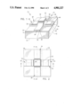
- FIG. 1 is a perspective view of one embodiment of a surface emitting laser constructed in accordance with teachings of the present invention
- FIG. 2 is a top plan view of the surface emitting laser of FIG. 1;
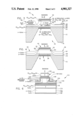
- FIG. 3 is a sectional view taken across line 3--3 of the surface emitting laser of FIG. 2;
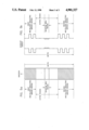
- FIG. 4 is a sectional view taken across line 4--4 of the surface emitting laser of FIG. 2;
- FIG. 5a illustrates a schematic cross-section of the surface emitting laser mirror and active regions with a quantum well region formed
- the active region in FIG. 5b is a graph illustrating the bandgap energy distribution corresponding to the schematic cross-section of FIG. 5a
- FIG. 6 is an alternate embodiment of a surface emitting laser of the present invention.
- the present invention comprises a novel and improved surface emitting laserutilizing transverse carrier injection into the active region of the optical cavity.
- one embodiment of the present invention reveals a surface emitting laser that is similar in structure to a conventional buried heterostructure laser.
- the structure of the one embodiment of the present invention differs in that a transverse masking stripe is deposited perpendicular to the lateral mesa stripe and then chemically etched. The resulting structure reveals a central portion of the lateral mesa stripe remaining at the original height while the end portions of the lateral mesa stripe have been chemically etched to a lowerthickness.
- An additional masking stripe is placed over one end portion of the lateral mesa stripe and extending up one side of the central portion of the lateral mesa stripe.
- a diffusion process is then performed at the unmasked portion of the lateral mesa stripe.
- the masking stripes are removed.
- Contacts are formed at the lateral mesa stripe end portions by depositing metal thereupon.
- a hole is then chemically etched through the substrate from the substrate backside, with the hole aligned with the central portion of lateral mesa stripe. Dielectric mirrors are then formed within the hole and on top of the mesa central portion.
- FIGS. 1 and 2 respectively illustrate one embodiment of the present invention in perspective and top plan views.
- the structure of surface emitting laser 10 is formed upon an n-type GaAs substrate 12.
- Substrate 12 has top and bottom surfaces respectively identified by the reference numerals 14 and 16.
- substrate 12 is prepared for use at top surface 14 for the fabrication of a device upon substrate top surface 14 by forming a buffer layer 18 thereupon.
- a buffer layer is formed upon a substrate top surface to overcome surface imperfections.
- Substrate top surface 14 is typically prepared by cleaning and polishing techniques prior to the formation of buffer layer 18 thereupon
- Buffer layer 18 is typically formed by growing a layer of lattice matched semiconductor material upon substrate top surface 14.
- buffer layer 18 is typically formed by growing a layer approximately 1.0 ⁇ m thick n-type GaAs upon substrate top surface14.
- the substrate may be chemically etched at one surfaceto form a top surface upon which the surface emitting laser may be fabricated.
- FIGS. 1 and 2 further illustrate lateral mesa stripe 20 which is comprised of a central portion 22 and a pair of end portions 24 and 26 formed upon buffer layer 18.
- Lateral mesa stripe central portion 22 extends above buffer layer 18 at a height greater than lateral mesa stripe end portions 24 and 26 which extend outwardly therefrom upon buffer layer 18.
- Lateral mesa stripe 20 is constructed from a barrier layer 28 formed upon buffer layer 18, an active layer 30 formed upon barrier layer 28, and another barrier layer 32 formed upon active layer 30.
- Barrier layer 32 and active layer 30 are chemically etched during the fabrication of surface emitting laser 10 to define lateral mesa stripe end portions 24 and 26.
- lateral mesa stripe central portion 22 is defined by an unetched portion of barrier layer 28, active layer 30 and barrier layer 32.
- Transverse stripes 34 and 36 are formed upon buffer layer 18 and extend outwardly upon buffer layer 18 substantially perpendicular to lateral mesastripe 20. Transverse stripes 34 and 36 abut against the sides of lateral mesa stripe central portion 22. Transverse stripes 34 and 36 are comprisedof a first confinement layer 38 formed upon buffer layer 18 which extends up the side walls of lateral mesa stripe 20. A second confinement layer 40is formed upon layer 38. Portions of first and second confinement layers 38and 40 are masked, then chemically etched to define transverse stripes 34 and 36.
- Hole 42 (FIG. 3) is formed in substrate 12, at substrate bottom surface 16,which extends through substrate 12 perpendicular to the plane of substrate bottom surface 16. Hole 42 is aligned with lateral mesa stripe central portion 22. Thus, hole 42 exposes barrier layer 28 within the region defining lateral mesa stripe center portion 22.
- Mirror 44 comprised of alternating layers of different refractive index dielectric materials, is formed upon barrier layer 32 in the region defined as lateral mesa stripe central portion 22.
- mirror 46 also comprised of alternating layers of different refractive index materials, is formed upon barrier layer 28 in the region defined as lateral mesa stripe central portion 22 within hole 42.
- barrier layer 28 which is typically comprised of undoped Al 0 .4 Ga 0 .6 As of a typical thickness in the range of 1,000-2,000 A.
- active layer 30 which is an n-type layer of GaAs preferably inthe range of approximately 2-3 ⁇ m in thickness.
- the lower portion of active layer 30, adjacent barrier layer 28, is heavily doped in n-type carrier concentration while the top portion is of more moderate n-type carrier concentration.
- barrierlayer 32 of undoped Al 0 .4 Ga 0 .6 As also of a thickness in the range of approximately 1,000-2,000 A.
- the material forming barrier layers 28 and 32 is of a higher bandgap, but lattice matched to the material of active layer 30.
- a lateral masking stripe (not shown) is placed on top of layer 32.
- the unmasked portions of barrier layer 32 and the corresponding underlying portions of active layer 30 and barrier layer28 are then chemically etched down to buffer layer 18, or if buffer layer 18 is not present then to substrate 12. Chemical etching of the unmasked portions of barrier layers 28 and 32, and active layer 30 thus defines lateral mesa stripe 20 beneath the lateral masking stripe.
- First confinement layer 38 comprised of lightly doped p-type Al 0 .4 Ga 0 .6 As of a thickness approximately 1.0 ⁇ m, is then formed upon buffer layer 18 and the sides of lateral mesa stripe 20.
- first confinement layer 38 Formed on top of,first confinement layer 38 is second confinement layer 40 which is comprised of lightly doped n-type Al 0 .4 Ga 0 .6 As of a thickness of approximately 1.0 ⁇ m.
- the lateral masking stripe is then removed and a transverse masking stripe (not shown) is positioned upon second confinement layer 40.
- the transverse masking stripe is positioned perpendicular to lateral mesa stripe 20 and is centrally oriented along the length of lateral mesa stripe 20.
- the unmasked portions of second confinement layer 40 and the corresponding underlying portions of first confinement layer 38 are chemically etched down to buffer layer 18.
- lateral masking stripe 20 is etched downinto the heavily doped n-type portion of active layer 30.
- the lateral mesa central stripe central portion 22 and end portions 24 and 26 are thus defined.
- Lateral mesa stripe central portion 22 is located beneath the transverse masking stripe and appears asa raised portion of lateral masking stripe 20.
- Lateral mesa stripe central portion 22, as formed, is approximately 2.0 ⁇ m in length and width.
- a diffusion masking stripe (not shown) is then placed upon lateral mesa stripe end portion 24, including the immediately adjacent side of lateral mesa stripe central portion 22 facing lateral mesa stripe end portion 24.
- a diffusion process is then performed so as to form a heavily doped p-typeZn diffusion region at the exposed side of lateral mesa stripe central portion 22 immediately adjacent lateral mesa stripe end portion 26 and along lateral mesa stripe end portion 26.
- the transverse masking stripe and the diffusion masking are then removed.
- Contacts or electrodes are then formed by depositing metal upon the top surface of active layer 30 in the lateral mesa stripe end portions 24 and 26.
- An AuSn metalization is performed at lateral mesa stripe end portion 24 so as to form contact 48.
- an AuCr metalization is performed upon lateral mesa stripe end portion 26 so as to form contact 50.
- Hole 42 (FIG. 3) is chemically etched from the underside of substrate 12 through substrate 12 and buffer layer 18, if present, to barrier layer 28.Hole 42 is centered under the lateral mesa stripe central portion 22. Mirrors 44 and 46 are then formed by depositing alternating layers of dielectric materials, such as TiO 2 and SiO 2 , upon the remaining portion of barrier layer 32 at lateral mesa stripe central portion 22, andwithin hole 42 upon barrier layer 28. Mirrors 44 and 46 are sometimes referred to in the art as distributed Bragg reflectors. By depositing mirrors 44 and 46 respectively upon barrier layers 32 and 28 after the diffusion into active layer 30 avoids damaging the mirrors during the diffusion process.
- surface emitting laser 10 is described with particular reference to semiconductor materials such as GaAs and Al 0 .4 Ga 0 .6 As, it is well known that other types of semiconductor materials may be utilized.
- the substrate may be InP, the high bandgap barrier layers InP,and the active layer InGaAsP.
- FIG. 3 illustrates surface emitting laser 10 in a sectional view taken across line 3--3 of FIG. 2.
- mirror 46 is formed upon barrier layer 28 within hole 46, while mirror 44 is formed upon barrier layer 32.
- a laser active region or optical cavity 52 is defined by active layer 30 within lateral mesa stripe central portion 22 between dielectric mirrors 44 and 46.
- the combination of mirrors 44 and 46 formed on opposite sides of optical cavity 52 define a resonant optical cavity.
- Current passing through the optical cavity between contacts 48 and 50 is transverse to thedirection of light emission from surface emitting laser 10.
- the light emission from surface emitting laser 10 is indicated by arrow 54.
- Current passing through optical cavity 52 during operation of surface emitting laser 10 is indicated by arrow 56.
- Light emission from surface emitting laser 10 is thus essentially perpendicular to a plane defined by substratetop surface 14.
- mirrors 44 and 46 be formed from dielectric materials, although other semiconductor materials may be used, as is well known in the art. Mirrors formed of alternating layers ofdielectric materials of differing refractive indices are known to be capable of reflectivities exceeding 99.9%. It is further preferred that a thin layer of higher bandgap lattice matched material, i.e., barrier layers 28 and 32, be grown between the lasing medium, i.e., active region or optical cavity 52, to provide current confinement away from the active region/mirror interface. Implementation of the barrier layers avoids carrier recombination at surface states and imperfections at the active region/mirror interface.
- Light emission may occur from either mirror.
- a lesser number of dielectric layer pairs are deposited upon the barrier layer to form the mirror from which light is tobe emitted.
- the total number of dielectric layer pairs be in the range of 20-30.
- FIG. 4 illustrates surface emitting laser 10 in a sectional view taken along line 4--4 of FIG. 2. The view in FIG. 4 is taken looking along the direction of current flow in the optical cavity 52.
- FIG. 4 illustrates in further detail the regrown first and second confinement layers 38 and 40 of transverse stripes 34 and 36 which abut against sides 58 and 60 of lateral mesa stripe 20 in the region of lateral mesa stripe central portion 22. Transverse stripes 34 and 36 extend outwardly perpendicularly from sides 58 and 60 upon buffer layer 18.
- First confinement layer 38 of transverse stripes 34 and 36 is a lightly doped p-type Al 0 .4 Ga 0 .6 As layer that is formed upon buffer layer 18, and along the sides of barrier layer 32, active layer 30 at optical cavity 52, and barrier layer 36.
- Second confinement layer 40 is a lightly doped n-type Al 0 .4 Ga 0 .6 As layer that overlies first confinement layer 38.
- First and second confinement layers 38 and 40 are integrally formed against optical cavity 52 so as to function as a reverse bias junction. Accordingly, first and second confinement layers 38 and 40 effectively block current from flowing around the sides or edges of optical cavity 52.
- FIGS. 1-4 injection is achieved transverse to the direction of light propagation. Accordingly, in the structure of the invention described with reference to FIGS. 1-4, there isno need to form an injecting contact at a p-side mirror as in the structuredisclosed in the previously referenced article of Iga et al. Furthermore, the p-type diffusion in the active layer is performed prior to mirror fabrication, thus avoiding mechanical deformation of the mirrors. Utilizing a cavity of length 2-3 ⁇ m will produce a more widely spaced longitudinal mode resulting in increased stability in single longitudinal mode operation.
- the structure of the surface emitting laser disclosed withreference to FIGS. 1-4 may be constructed using epitaxy techniques well known in the art. These techniques include molecular beam epitaxy (MBE) ormetalorganic chemical vapor deposition (MOCVD) and are known for accuracy and reproducibility in the growing of layers on the order of 1,000A or less.
- MBE molecular beam epitaxy
- MOCVD metalorganic chemical vapor deposition
- quantum wells may be introduced therein. Quantum wells are formed in the active layer by "shuttering” or selectively introducing an aluminum component, along with the Ga and As components during the epitaxytechnique formation of the active layer.
- Quantum wells formed in the optical cavity active layer willlower the lasing threshold current, due to the reduced density of states inthe wells.
- Quantum wells formed in the optical cavity active layer also increase the wavelength of emission, due to the reduced bandgap in the active layer. Increased emission wavelength will thus allow the lowest bandgap in the multilayer dielectric mirrors to be lowered.
- a reduction inthe lowest bandgap in the multilayer dielectric mirrors will permit the index of refraction to increase and thus improve the reflectivity of the mirrors.
- FIG. 5a is a schematic diagram of an active region structure similar to theembodiment of FIGS. 1-4 while incorporating a quantum well region while disregarding the barrier layers.
- FIG. 5b is a graph illustrating the corresponding bandgap energy versus depth for the structure in FIG. 5a.
- FIG. 6 illustrates an alternate embodiment of the present invention constructed using MBE or MOCVD techniques. Use of these techniques enablesthe growth of semiconductor mirrors in alternating layers of high and low index materials which are lattice matched to the substrate and/or active layer.
- FIG. 6 illustrates, in cross-section, surface emitting laser 110.
- Surface emitting laser 110 is comprised of an n-type GaAs substrate 112 which typically includes a buffer layer (not shown) formed at surface 114.Alternating layers of Al 0 .6 Ga 0 .4 As and GaAs are sequentially grown upon the substrate top surface 114 or buffer layer, if included, to form a multilayer semiconductor mirror or distributed Bragg reflector 116.
- the laser active region is formed by growing an n-type GaAs active layer 118 in the range of 2-3 ⁇ m thick on top of mirror stack 116. Alternating layers of Al 0 .4 Ga 0 .6 As and GaAs are formed on top of active layer 118 to form a multilayer mirror or distributed Bragg reflector 120.
- a mesa is then formed in the structure typically by first forming a circular mask on top of mirror 120. The unmasked portion of mirror 116, and the underlying portion of active layer 118, is chemically etched to leave mesa 122. A diffusion region 124 is then formed about the side of mesa 122 and in the thinner outer portion of active layer 118 adjacent mesa 122. Diffusion region 124 is formed by diffusing p-type Zn in the active layer 118.
- Dielectric layer 126 is deposited on side 128 of mesa 122 at active layer 118 while overlappinga portion of mirror 120. Dielectric layer 126 extends radially outwardly from mesa 122 upon exposed top surface 130 of active layer 118 immediatelyadjacent mesa 122.
- the refractive index of the dielectric material is chosen to match that of active region 132, i.e. the portion of active layer 118 within mesa 122, so as to reduce the effects of optical scattering at the boundary thereof.
- dielectric layer 126 may be replaced by a regrowth of a higher bandgap lattice matched p-type GaAs layer about mesa 122 followed by the regrowth of a n-type layer of GaAs.
- Contact 134 is formed by a AuCr metalization upon the remaining exposed topsurface 130 of active layer 118, with the metalization overlapping dielectric layer 126.
- Contact 136 is formed of AuSn metalization upon substrate bottom surface 138.
Abstract
Description
Claims (16)
Priority Applications (2)
| Application Number | Priority Date | Filing Date | Title |
|---|---|---|---|
| US07/261,413 US4901327A (en) | 1988-10-24 | 1988-10-24 | Transverse injection surface emitting laser |
| US07/410,342 US4943970A (en) | 1988-10-24 | 1989-09-21 | Surface emitting laser |
Applications Claiming Priority (1)
| Application Number | Priority Date | Filing Date | Title |
|---|---|---|---|
| US07/261,413 US4901327A (en) | 1988-10-24 | 1988-10-24 | Transverse injection surface emitting laser |
Related Child Applications (1)
| Application Number | Title | Priority Date | Filing Date |
|---|---|---|---|
| US07/410,342 Division US4943970A (en) | 1988-10-24 | 1989-09-21 | Surface emitting laser |
Publications (1)
| Publication Number | Publication Date |
|---|---|
| US4901327A true US4901327A (en) | 1990-02-13 |
Family
ID=22993198
Family Applications (1)
| Application Number | Title | Priority Date | Filing Date |
|---|---|---|---|
| US07/261,413 Expired - Fee Related US4901327A (en) | 1988-10-24 | 1988-10-24 | Transverse injection surface emitting laser |
Country Status (1)
| Country | Link |
|---|---|
| US (1) | US4901327A (en) |
Cited By (40)
| Publication number | Priority date | Publication date | Assignee | Title |
|---|---|---|---|---|
| US5023944A (en) * | 1989-09-05 | 1991-06-11 | General Dynamics Corp./Electronics Division | Optical resonator structures |
| US5068869A (en) * | 1987-06-19 | 1991-11-26 | Lockheed Missiles & Space Company, Inc. | Surface-emitting laser diode |
| US5159603A (en) * | 1991-06-05 | 1992-10-27 | United States Of America As Represented By The Administrator, National Aeronautics And Space Administration | Quantum well, beam deflecting surface emitting lasers |
| US5239190A (en) * | 1989-01-31 | 1993-08-24 | Canon Kabushiki Kaisha | Light emitting device and method for manufacturing the same |
| US5245622A (en) * | 1992-05-07 | 1993-09-14 | Bandgap Technology Corporation | Vertical-cavity surface-emitting lasers with intra-cavity structures |
| US5253263A (en) * | 1992-03-12 | 1993-10-12 | Trw Inc. | High-power surface-emitting semiconductor injection laser with etched internal 45 degree and 90 degree micromirrors |
| US5258990A (en) * | 1991-11-07 | 1993-11-02 | The United States Of America As Represented By The Secretary Of The United States Department Of Energy | Visible light surface emitting semiconductor laser |
| EP0587911A1 (en) * | 1992-03-31 | 1994-03-23 | The Furukawa Electric Co., Ltd. | Semiconductor laser device |
| GB2304993A (en) * | 1995-08-23 | 1997-03-26 | Toshiba Cambridge Res Center | Semiconductor laser device |
| US5774487A (en) * | 1996-10-16 | 1998-06-30 | Honeywell Inc. | Filamented multi-wavelength vertical-cavity surface emitting laser |
| US5978401A (en) * | 1995-10-25 | 1999-11-02 | Honeywell Inc. | Monolithic vertical cavity surface emitting laser and resonant cavity photodetector transceiver |
| US20020085610A1 (en) * | 2000-12-29 | 2002-07-04 | Morgan Robert A. | Spatially modulated reflector for an optoelectronic device |
| US20020106160A1 (en) * | 2000-12-29 | 2002-08-08 | Honeywell International Inc. | Resonant reflector for increased wavelength and polarization control |
| US6606199B2 (en) | 2001-10-10 | 2003-08-12 | Honeywell International Inc. | Graded thickness optical element and method of manufacture therefor |
| US20040042518A1 (en) * | 2002-09-03 | 2004-03-04 | Tatum James A. | Single mode VCSEL |
| US20040066819A1 (en) * | 2000-11-28 | 2004-04-08 | Johnson Ralph H. | Versatile method and system for single mode VCSELs |
| US20040081215A1 (en) * | 2002-10-28 | 2004-04-29 | Honeywell International Inc. | Distributed bragg reflector for optoelectronic device |
| US20040101009A1 (en) * | 2002-11-21 | 2004-05-27 | Honeywell International Inc. | Long wavelength VCSEL with tunnel junction, and implant |
| US6782027B2 (en) | 2000-12-29 | 2004-08-24 | Finisar Corporation | Resonant reflector for use with optoelectronic devices |
| US20040222363A1 (en) * | 2003-05-07 | 2004-11-11 | Honeywell International Inc. | Connectorized optical component misalignment detection system |
| US20040247250A1 (en) * | 2003-06-03 | 2004-12-09 | Honeywell International Inc. | Integrated sleeve pluggable package |
| US20040264855A1 (en) * | 2003-06-30 | 2004-12-30 | Bo Su Chen | Optical system with reduced back reflection |
| US20040264530A1 (en) * | 2003-06-27 | 2004-12-30 | Honeywell International Inc. | VCSEL having thermal management |
| US20040264536A1 (en) * | 2003-06-27 | 2004-12-30 | Honeywell International Inc. | Dielectric VCSEL gain guide |
| US20050013542A1 (en) * | 2003-07-16 | 2005-01-20 | Honeywell International Inc. | Coupler having reduction of reflections to light source |
| US20050013553A1 (en) * | 2003-07-16 | 2005-01-20 | Honeywell International Inc. | Optical coupling system |
| US20050013539A1 (en) * | 2003-07-17 | 2005-01-20 | Honeywell International Inc. | Optical coupling system |
| US20050014390A1 (en) * | 2003-07-18 | 2005-01-20 | Honeywell International Inc. | Edge bead control method and apparatus |
| US20050031011A1 (en) * | 2000-11-28 | 2005-02-10 | Biard James R. | Electron affinity engineered VCSELs |
| US20050036533A1 (en) * | 2000-12-29 | 2005-02-17 | Honeywell To Finisar | Tunable detector |
| US20050092710A1 (en) * | 2003-10-29 | 2005-05-05 | Biard James R. | Long wavelength VCSEL device processing |
| US20050201680A1 (en) * | 2003-06-30 | 2005-09-15 | Cox James A. | Methods for signal transmission in optical fiber |
| US20060045162A1 (en) * | 2004-08-31 | 2006-03-02 | Finisar Corporation | Distributed bragg reflector for optoelectronic device |
| US20060056762A1 (en) * | 2003-07-02 | 2006-03-16 | Honeywell International Inc. | Lens optical coupler |
| US7054345B2 (en) | 2003-06-27 | 2006-05-30 | Finisar Corporation | Enhanced lateral oxidation |
| US20060268954A1 (en) * | 2004-08-31 | 2006-11-30 | Johnson Ralph H | Light emitting semiconductor device having an electrical confinement barrier near the active region |
| US7298942B2 (en) | 2003-06-06 | 2007-11-20 | Finisar Corporation | Pluggable optical optic system having a lens fiber stop |
| US20080023688A1 (en) * | 2006-07-31 | 2008-01-31 | Finisar Corporation | Efficient carrier injection in a semiconductor device |
| US7433381B2 (en) | 2003-06-25 | 2008-10-07 | Finisar Corporation | InP based long wavelength VCSEL |
| US8031752B1 (en) | 2007-04-16 | 2011-10-04 | Finisar Corporation | VCSEL optimized for high speed data |
Citations (15)
| Publication number | Priority date | Publication date | Assignee | Title |
|---|---|---|---|---|
| US3703670A (en) * | 1969-02-28 | 1972-11-21 | Corning Glass Works | Electroluminescent diode configuration and method of forming the same |
| US3983509A (en) * | 1975-04-25 | 1976-09-28 | Xerox Corporation | Distributed feedback diode laser |
| US4309670A (en) * | 1979-09-13 | 1982-01-05 | Xerox Corporation | Transverse light emitting electroluminescent devices |
| US4512022A (en) * | 1982-07-13 | 1985-04-16 | At&T Bell Laboratories | Semiconductor laser having graded index waveguide |
| JPS614291A (en) * | 1984-06-19 | 1986-01-10 | Agency Of Ind Science & Technol | Surface light-emission laser |
| US4633476A (en) * | 1984-11-16 | 1986-12-30 | Spectra Diode Laboratories, Inc. | Semiconductor laser with internal reflectors and vertical output |
| US4644553A (en) * | 1983-11-22 | 1987-02-17 | U.S. Philips Corporation | Semiconductor laser with lateral injection |
| US4660207A (en) * | 1984-11-21 | 1987-04-21 | Northern Telecom Limited | Surface-emitting light emitting device |
| US4665527A (en) * | 1983-11-09 | 1987-05-12 | Kokusai Denshin Denwa Kabushiki Kaisha | Distributed feedback semiconductor laser |
| US4675877A (en) * | 1985-02-14 | 1987-06-23 | Northern Telecom Limited | Bragg distributed feedback surface emitting laser |
| US4675875A (en) * | 1983-08-18 | 1987-06-23 | Mitsubishi Denki Kabushiki Kaisha | Surface emitting semiconductor laser |
| US4675876A (en) * | 1985-02-14 | 1987-06-23 | Northern Telecom Limited | Bragg distributed feedback surface emitting laser |
| US4706101A (en) * | 1984-10-27 | 1987-11-10 | Kabushiki Kaisha Toshiba | Light emitting diode formed of a compound semiconductor material |
| US4760578A (en) * | 1985-11-29 | 1988-07-26 | Matsushita Electric Industrial Co., Ltd. | Semiconductor laser with a controllable transmittance layer |
| US4797890A (en) * | 1985-12-24 | 1989-01-10 | Mitsubishi Cable Industries, Ltd. | Semiconductor light emitting device with vertical light emission |
-
1988
- 1988-10-24 US US07/261,413 patent/US4901327A/en not_active Expired - Fee Related
Patent Citations (15)
| Publication number | Priority date | Publication date | Assignee | Title |
|---|---|---|---|---|
| US3703670A (en) * | 1969-02-28 | 1972-11-21 | Corning Glass Works | Electroluminescent diode configuration and method of forming the same |
| US3983509A (en) * | 1975-04-25 | 1976-09-28 | Xerox Corporation | Distributed feedback diode laser |
| US4309670A (en) * | 1979-09-13 | 1982-01-05 | Xerox Corporation | Transverse light emitting electroluminescent devices |
| US4512022A (en) * | 1982-07-13 | 1985-04-16 | At&T Bell Laboratories | Semiconductor laser having graded index waveguide |
| US4675875A (en) * | 1983-08-18 | 1987-06-23 | Mitsubishi Denki Kabushiki Kaisha | Surface emitting semiconductor laser |
| US4665527A (en) * | 1983-11-09 | 1987-05-12 | Kokusai Denshin Denwa Kabushiki Kaisha | Distributed feedback semiconductor laser |
| US4644553A (en) * | 1983-11-22 | 1987-02-17 | U.S. Philips Corporation | Semiconductor laser with lateral injection |
| JPS614291A (en) * | 1984-06-19 | 1986-01-10 | Agency Of Ind Science & Technol | Surface light-emission laser |
| US4706101A (en) * | 1984-10-27 | 1987-11-10 | Kabushiki Kaisha Toshiba | Light emitting diode formed of a compound semiconductor material |
| US4633476A (en) * | 1984-11-16 | 1986-12-30 | Spectra Diode Laboratories, Inc. | Semiconductor laser with internal reflectors and vertical output |
| US4660207A (en) * | 1984-11-21 | 1987-04-21 | Northern Telecom Limited | Surface-emitting light emitting device |
| US4675877A (en) * | 1985-02-14 | 1987-06-23 | Northern Telecom Limited | Bragg distributed feedback surface emitting laser |
| US4675876A (en) * | 1985-02-14 | 1987-06-23 | Northern Telecom Limited | Bragg distributed feedback surface emitting laser |
| US4760578A (en) * | 1985-11-29 | 1988-07-26 | Matsushita Electric Industrial Co., Ltd. | Semiconductor laser with a controllable transmittance layer |
| US4797890A (en) * | 1985-12-24 | 1989-01-10 | Mitsubishi Cable Industries, Ltd. | Semiconductor light emitting device with vertical light emission |
Non-Patent Citations (6)
| Title |
|---|
| High Reflectivity GaAs AlGaAs Mirrors Fabricated by Metalorganic Chemical Vapor Deposition by R. L Thornton et al., Applied Physics Letters, vol. 45, No. 10, pp. 1028 1030, Nov. 15, 1984. * |
| High Reflectivity GaAs-AlGaAs Mirrors Fabricated by Metalorganic Chemical Vapor Deposition by R. L Thornton et al., Applied Physics Letters, vol. 45, No. 10, pp. 1028-1030, Nov. 15, 1984. |
| Room Temperature Pulsed Oscillation of GaAlAs/GaAs Surface Emitting Injection Laser by K. Iga et al., App. Physics Letters, vol. 45, (No. 10 pp. 348 350, Aug. 15, 1984). * |
| Room-Temperature Pulsed Oscillation of GaAlAs/GaAs Surface Emitting Injection Laser by K. Iga et al., App. Physics Letters, vol. 45, (No. 10 pp. 348-350, Aug. 15, 1984). |
| Surface Emitting Laser Diode with Vertical GaAs,GaAlAs Quarter Wavelength Multilayers and Lateral Buried Heterostructure by Mutsuo Ogura et al., Applied Physics Letters, vol. 51, No. 21, pp. 1655 1657 Nov. 23, 1987. * |
| Surface-Emitting Laser Diode with Vertical GaAs,GaAlAs Quarter-Wavelength Multilayers and Lateral Buried Heterostructure by Mutsuo Ogura et al., Applied Physics Letters, vol. 51, No. 21, pp. 1655-1657 Nov. 23, 1987. |
Cited By (74)
| Publication number | Priority date | Publication date | Assignee | Title |
|---|---|---|---|---|
| US5068869A (en) * | 1987-06-19 | 1991-11-26 | Lockheed Missiles & Space Company, Inc. | Surface-emitting laser diode |
| US5239190A (en) * | 1989-01-31 | 1993-08-24 | Canon Kabushiki Kaisha | Light emitting device and method for manufacturing the same |
| US5023944A (en) * | 1989-09-05 | 1991-06-11 | General Dynamics Corp./Electronics Division | Optical resonator structures |
| US5159603A (en) * | 1991-06-05 | 1992-10-27 | United States Of America As Represented By The Administrator, National Aeronautics And Space Administration | Quantum well, beam deflecting surface emitting lasers |
| US5642376A (en) * | 1991-11-07 | 1997-06-24 | Vixel Corporation | Visible light surface emitting semiconductor laser |
| US5258990A (en) * | 1991-11-07 | 1993-11-02 | The United States Of America As Represented By The Secretary Of The United States Department Of Energy | Visible light surface emitting semiconductor laser |
| US5253263A (en) * | 1992-03-12 | 1993-10-12 | Trw Inc. | High-power surface-emitting semiconductor injection laser with etched internal 45 degree and 90 degree micromirrors |
| EP0587911A1 (en) * | 1992-03-31 | 1994-03-23 | The Furukawa Electric Co., Ltd. | Semiconductor laser device |
| EP0587911A4 (en) * | 1992-03-31 | 1994-08-31 | The Furukawa Electric Co., Ltd. | |
| US5544189A (en) * | 1992-03-31 | 1996-08-06 | The Furukawa Electric Co., Ltd. | Semiconductor laser device |
| US5245622A (en) * | 1992-05-07 | 1993-09-14 | Bandgap Technology Corporation | Vertical-cavity surface-emitting lasers with intra-cavity structures |
| GB2304993A (en) * | 1995-08-23 | 1997-03-26 | Toshiba Cambridge Res Center | Semiconductor laser device |
| GB2304993B (en) * | 1995-08-23 | 1997-08-06 | Toshiba Cambridge Res Center | Semiconductor device |
| US5978401A (en) * | 1995-10-25 | 1999-11-02 | Honeywell Inc. | Monolithic vertical cavity surface emitting laser and resonant cavity photodetector transceiver |
| US5774487A (en) * | 1996-10-16 | 1998-06-30 | Honeywell Inc. | Filamented multi-wavelength vertical-cavity surface emitting laser |
| US7065124B2 (en) | 2000-11-28 | 2006-06-20 | Finlsar Corporation | Electron affinity engineered VCSELs |
| US20040213311A1 (en) * | 2000-11-28 | 2004-10-28 | Johnson Ralph H | Single mode vertical cavity surface emitting laser |
| US6905900B1 (en) | 2000-11-28 | 2005-06-14 | Finisar Corporation | Versatile method and system for single mode VCSELs |
| US7221691B2 (en) | 2000-11-28 | 2007-05-22 | Finisar Corporation | Versatile method and system for single mode VCSELs |
| US20040066819A1 (en) * | 2000-11-28 | 2004-04-08 | Johnson Ralph H. | Versatile method and system for single mode VCSELs |
| US20040066820A1 (en) * | 2000-11-28 | 2004-04-08 | Johnson Ralph H. | Versatile method and system for single mode VCSELs |
| US20050031011A1 (en) * | 2000-11-28 | 2005-02-10 | Biard James R. | Electron affinity engineered VCSELs |
| US7308011B2 (en) | 2000-11-28 | 2007-12-11 | Finisar Corporation | Versatile method and system for single mode VCSELs |
| US6782027B2 (en) | 2000-12-29 | 2004-08-24 | Finisar Corporation | Resonant reflector for use with optoelectronic devices |
| US20020085610A1 (en) * | 2000-12-29 | 2002-07-04 | Morgan Robert A. | Spatially modulated reflector for an optoelectronic device |
| US20040191941A1 (en) * | 2000-12-29 | 2004-09-30 | Morgan Robert A. | Method for producing laser with resonant reflector |
| US20040188695A1 (en) * | 2000-12-29 | 2004-09-30 | Morgan Robert A. | Laser with resonant reflector |
| US20050036533A1 (en) * | 2000-12-29 | 2005-02-17 | Honeywell To Finisar | Tunable detector |
| US6727520B2 (en) | 2000-12-29 | 2004-04-27 | Honeywell International Inc. | Spatially modulated reflector for an optoelectronic device |
| US7266135B2 (en) | 2000-12-29 | 2007-09-04 | Finisar Corporation | Method for producing laser with resonant reflector |
| US6836501B2 (en) | 2000-12-29 | 2004-12-28 | Finisar Corporation | Resonant reflector for increased wavelength and polarization control |
| US8599897B2 (en) | 2000-12-29 | 2013-12-03 | Finisar Corporation | Tunable detector |
| US7760786B2 (en) | 2000-12-29 | 2010-07-20 | Finisar Corporation | Laser with resonant reflector |
| US20020106160A1 (en) * | 2000-12-29 | 2002-08-08 | Honeywell International Inc. | Resonant reflector for increased wavelength and polarization control |
| US7288421B2 (en) | 2000-12-29 | 2007-10-30 | Finisar Corporation | Method for forming an optoelectronic device having an isolation layer |
| US6606199B2 (en) | 2001-10-10 | 2003-08-12 | Honeywell International Inc. | Graded thickness optical element and method of manufacture therefor |
| US6965626B2 (en) | 2002-09-03 | 2005-11-15 | Finisar Corporation | Single mode VCSEL |
| US20040042518A1 (en) * | 2002-09-03 | 2004-03-04 | Tatum James A. | Single mode VCSEL |
| US20040081215A1 (en) * | 2002-10-28 | 2004-04-29 | Honeywell International Inc. | Distributed bragg reflector for optoelectronic device |
| US6990135B2 (en) | 2002-10-28 | 2006-01-24 | Finisar Corporation | Distributed bragg reflector for optoelectronic device |
| US7251264B2 (en) | 2002-10-28 | 2007-07-31 | Finisar Corporation | Distributed bragg reflector for optoelectronic device |
| US20050190812A1 (en) * | 2002-10-28 | 2005-09-01 | Johnson Ralph H. | Distributed bragg reflector for optoelectronic device |
| US6813293B2 (en) | 2002-11-21 | 2004-11-02 | Finisar Corporation | Long wavelength VCSEL with tunnel junction, and implant |
| US20040101009A1 (en) * | 2002-11-21 | 2004-05-27 | Honeywell International Inc. | Long wavelength VCSEL with tunnel junction, and implant |
| US20040222363A1 (en) * | 2003-05-07 | 2004-11-11 | Honeywell International Inc. | Connectorized optical component misalignment detection system |
| US20040247250A1 (en) * | 2003-06-03 | 2004-12-09 | Honeywell International Inc. | Integrated sleeve pluggable package |
| US7298942B2 (en) | 2003-06-06 | 2007-11-20 | Finisar Corporation | Pluggable optical optic system having a lens fiber stop |
| US7433381B2 (en) | 2003-06-25 | 2008-10-07 | Finisar Corporation | InP based long wavelength VCSEL |
| US7075962B2 (en) | 2003-06-27 | 2006-07-11 | Finisar Corporation | VCSEL having thermal management |
| US7277461B2 (en) | 2003-06-27 | 2007-10-02 | Finisar Corporation | Dielectric VCSEL gain guide |
| US20040264530A1 (en) * | 2003-06-27 | 2004-12-30 | Honeywell International Inc. | VCSEL having thermal management |
| US20040264536A1 (en) * | 2003-06-27 | 2004-12-30 | Honeywell International Inc. | Dielectric VCSEL gain guide |
| US7054345B2 (en) | 2003-06-27 | 2006-05-30 | Finisar Corporation | Enhanced lateral oxidation |
| US7139454B2 (en) | 2003-06-30 | 2006-11-21 | Finisar Corporation | Methods for signal transmission in optical fiber |
| US6961489B2 (en) | 2003-06-30 | 2005-11-01 | Finisar Corporation | High speed optical system |
| US20040264855A1 (en) * | 2003-06-30 | 2004-12-30 | Bo Su Chen | Optical system with reduced back reflection |
| US7149383B2 (en) | 2003-06-30 | 2006-12-12 | Finisar Corporation | Optical system with reduced back reflection |
| US20050201680A1 (en) * | 2003-06-30 | 2005-09-15 | Cox James A. | Methods for signal transmission in optical fiber |
| US20060056762A1 (en) * | 2003-07-02 | 2006-03-16 | Honeywell International Inc. | Lens optical coupler |
| US20050013553A1 (en) * | 2003-07-16 | 2005-01-20 | Honeywell International Inc. | Optical coupling system |
| US7210857B2 (en) | 2003-07-16 | 2007-05-01 | Finisar Corporation | Optical coupling system |
| US20050013542A1 (en) * | 2003-07-16 | 2005-01-20 | Honeywell International Inc. | Coupler having reduction of reflections to light source |
| US20050013539A1 (en) * | 2003-07-17 | 2005-01-20 | Honeywell International Inc. | Optical coupling system |
| US20050014390A1 (en) * | 2003-07-18 | 2005-01-20 | Honeywell International Inc. | Edge bead control method and apparatus |
| US6887801B2 (en) | 2003-07-18 | 2005-05-03 | Finisar Corporation | Edge bead control method and apparatus |
| US7031363B2 (en) | 2003-10-29 | 2006-04-18 | Finisar Corporation | Long wavelength VCSEL device processing |
| US20050092710A1 (en) * | 2003-10-29 | 2005-05-05 | Biard James R. | Long wavelength VCSEL device processing |
| US20060268954A1 (en) * | 2004-08-31 | 2006-11-30 | Johnson Ralph H | Light emitting semiconductor device having an electrical confinement barrier near the active region |
| US7596165B2 (en) | 2004-08-31 | 2009-09-29 | Finisar Corporation | Distributed Bragg Reflector for optoelectronic device |
| US7920612B2 (en) | 2004-08-31 | 2011-04-05 | Finisar Corporation | Light emitting semiconductor device having an electrical confinement barrier near the active region |
| US20060045162A1 (en) * | 2004-08-31 | 2006-03-02 | Finisar Corporation | Distributed bragg reflector for optoelectronic device |
| US20080023688A1 (en) * | 2006-07-31 | 2008-01-31 | Finisar Corporation | Efficient carrier injection in a semiconductor device |
| US7829912B2 (en) | 2006-07-31 | 2010-11-09 | Finisar Corporation | Efficient carrier injection in a semiconductor device |
| US8031752B1 (en) | 2007-04-16 | 2011-10-04 | Finisar Corporation | VCSEL optimized for high speed data |
Similar Documents
| Publication | Publication Date | Title |
|---|---|---|
| US4901327A (en) | Transverse injection surface emitting laser | |
| US4943970A (en) | Surface emitting laser | |
| US5045500A (en) | Method of making a semiconductor laser | |
| EP0858137B1 (en) | Surface emitting laser device and its method of manufacture | |
| US5068869A (en) | Surface-emitting laser diode | |
| US4633476A (en) | Semiconductor laser with internal reflectors and vertical output | |
| EP0115390A2 (en) | Semiconductor lasers | |
| US7532654B2 (en) | Laser diode | |
| US4845725A (en) | Window laser with high power reduced divergence output | |
| US4278949A (en) | Semiconductor laser structure and manufacture | |
| US4803691A (en) | Lateral superradiance suppressing diode laser bar | |
| KR100626891B1 (en) | Surface-Emitting Semiconductor Laser | |
| US4831630A (en) | Phased-locked window lasers | |
| US4416012A (en) | W-Guide buried heterostructure laser | |
| US5953358A (en) | Semiconductor laser device | |
| JPS63188983A (en) | Semiconductor light emitting device | |
| EP0422941B1 (en) | Method of manufacturing a window structure semiconductor laser | |
| US4759025A (en) | Window structure semiconductor laser | |
| US5185289A (en) | Process for the selective growth of GaAs | |
| US4821278A (en) | Inverted channel substrate planar semiconductor laser | |
| JP4155664B2 (en) | Semiconductor laser device | |
| US5329134A (en) | Superluminescent diode having a quantum well and cavity length dependent threshold current | |
| GB2095474A (en) | Semiconductor light emitting devices | |
| JP2927661B2 (en) | Super luminescent diode element and method of manufacturing the same | |
| EP0348540B1 (en) | Process for the selective growth of gaas |
Legal Events
| Date | Code | Title | Description |
|---|---|---|---|
| AS | Assignment |
Owner name: GENERAL DYNAMICS CORPORATION, ELECTRONICS DIVISION Free format text: ASSIGNMENT OF ASSIGNORS INTEREST.;ASSIGNOR:BRADLEY, ERIC M.;REEL/FRAME:004970/0451 Effective date: 19881018 Owner name: GENERAL DYNAMICS CORPORATION, ELECTRONICS DIVISION Free format text: ASSIGNMENT OF ASSIGNORS INTEREST;ASSIGNOR:BRADLEY, ERIC M.;REEL/FRAME:004970/0451 Effective date: 19881018 |
|
| AS | Assignment |
Owner name: TACAN CORPORATION, CALIFORNIA Free format text: ASSIGNMENT OF ASSIGNORS INTEREST.;ASSIGNOR:GENERAL DYNAMICS CORPORATION ELECTRONICS DIVISION;REEL/FRAME:005947/0158 Effective date: 19911203 |
|
| FEPP | Fee payment procedure |
Free format text: PAYOR NUMBER ASSIGNED (ORIGINAL EVENT CODE: ASPN); ENTITY STATUS OF PATENT OWNER: SMALL ENTITY |
|
| FEPP | Fee payment procedure |
Free format text: PAT HOLDER CLAIMS SMALL ENTITY STATUS - SMALL BUSINESS (ORIGINAL EVENT CODE: SM02); ENTITY STATUS OF PATENT OWNER: SMALL ENTITY Free format text: PAYER NUMBER DE-ASSIGNED (ORIGINAL EVENT CODE: RMPN); ENTITY STATUS OF PATENT OWNER: SMALL ENTITY |
|
| FPAY | Fee payment |
Year of fee payment: 4 |
|
| SULP | Surcharge for late payment | ||
| REMI | Maintenance fee reminder mailed | ||
| LAPS | Lapse for failure to pay maintenance fees | ||
| FP | Lapsed due to failure to pay maintenance fee |
Effective date: 19980218 |
|
| AS | Assignment |
Owner name: UNION BANK OF CALIFORNIA, N.A., CALIFORNIA Free format text: SECURITY AGREEMENT;ASSIGNOR:TACAN CORPORATION;REEL/FRAME:009703/0068 Effective date: 19981230 |
|
| AS | Assignment |
Owner name: TACAN CORPORATION, CALIFORNIA Free format text: SECURITY INTEREST;ASSIGNOR:UNION BANK OF CALIFORNIA N.A.;REEL/FRAME:010892/0422 Effective date: 19990708 |
|
| STCH | Information on status: patent discontinuation |
Free format text: PATENT EXPIRED DUE TO NONPAYMENT OF MAINTENANCE FEES UNDER 37 CFR 1.362 |