US4700276A - Ultra high density pad array chip carrier - Google Patents
Ultra high density pad array chip carrier Download PDFInfo
- Publication number
- US4700276A US4700276A US06/816,164 US81616486A US4700276A US 4700276 A US4700276 A US 4700276A US 81616486 A US81616486 A US 81616486A US 4700276 A US4700276 A US 4700276A
- Authority
- US
- United States
- Prior art keywords
- chip carrier
- ceramic substrate
- carrier arrangement
- dielectric layer
- flexible dielectric
- Prior art date
- Legal status (The legal status is an assumption and is not a legal conclusion. Google has not performed a legal analysis and makes no representation as to the accuracy of the status listed.)
- Expired - Fee Related
Links
Images


Classifications
-
- H—ELECTRICITY
- H01—ELECTRIC ELEMENTS
- H01L—SEMICONDUCTOR DEVICES NOT COVERED BY CLASS H10
- H01L21/00—Processes or apparatus adapted for the manufacture or treatment of semiconductor or solid state devices or of parts thereof
- H01L21/02—Manufacture or treatment of semiconductor devices or of parts thereof
- H01L21/04—Manufacture or treatment of semiconductor devices or of parts thereof the devices having at least one potential-jump barrier or surface barrier, e.g. PN junction, depletion layer or carrier concentration layer
- H01L21/48—Manufacture or treatment of parts, e.g. containers, prior to assembly of the devices, using processes not provided for in a single one of the subgroups H01L21/06 - H01L21/326
- H01L21/4814—Conductive parts
- H01L21/4846—Leads on or in insulating or insulated substrates, e.g. metallisation
-
- H—ELECTRICITY
- H01—ELECTRIC ELEMENTS
- H01L—SEMICONDUCTOR DEVICES NOT COVERED BY CLASS H10
- H01L23/00—Details of semiconductor or other solid state devices
- H01L23/48—Arrangements for conducting electric current to or from the solid state body in operation, e.g. leads, terminal arrangements ; Selection of materials therefor
- H01L23/488—Arrangements for conducting electric current to or from the solid state body in operation, e.g. leads, terminal arrangements ; Selection of materials therefor consisting of soldered or bonded constructions
- H01L23/498—Leads, i.e. metallisations or lead-frames on insulating substrates, e.g. chip carriers
- H01L23/49827—Via connections through the substrates, e.g. pins going through the substrate, coaxial cables
-
- H—ELECTRICITY
- H01—ELECTRIC ELEMENTS
- H01L—SEMICONDUCTOR DEVICES NOT COVERED BY CLASS H10
- H01L2224/00—Indexing scheme for arrangements for connecting or disconnecting semiconductor or solid-state bodies and methods related thereto as covered by H01L24/00
- H01L2224/01—Means for bonding being attached to, or being formed on, the surface to be connected, e.g. chip-to-package, die-attach, "first-level" interconnects; Manufacturing methods related thereto
- H01L2224/42—Wire connectors; Manufacturing methods related thereto
- H01L2224/44—Structure, shape, material or disposition of the wire connectors prior to the connecting process
- H01L2224/45—Structure, shape, material or disposition of the wire connectors prior to the connecting process of an individual wire connector
- H01L2224/45001—Core members of the connector
- H01L2224/45099—Material
- H01L2224/451—Material with a principal constituent of the material being a metal or a metalloid, e.g. boron (B), silicon (Si), germanium (Ge), arsenic (As), antimony (Sb), tellurium (Te) and polonium (Po), and alloys thereof
-
- H—ELECTRICITY
- H01—ELECTRIC ELEMENTS
- H01L—SEMICONDUCTOR DEVICES NOT COVERED BY CLASS H10
- H01L2224/00—Indexing scheme for arrangements for connecting or disconnecting semiconductor or solid-state bodies and methods related thereto as covered by H01L24/00
- H01L2224/01—Means for bonding being attached to, or being formed on, the surface to be connected, e.g. chip-to-package, die-attach, "first-level" interconnects; Manufacturing methods related thereto
- H01L2224/42—Wire connectors; Manufacturing methods related thereto
- H01L2224/47—Structure, shape, material or disposition of the wire connectors after the connecting process
- H01L2224/48—Structure, shape, material or disposition of the wire connectors after the connecting process of an individual wire connector
- H01L2224/4805—Shape
- H01L2224/4809—Loop shape
- H01L2224/48091—Arched
-
- H—ELECTRICITY
- H01—ELECTRIC ELEMENTS
- H01L—SEMICONDUCTOR DEVICES NOT COVERED BY CLASS H10
- H01L2224/00—Indexing scheme for arrangements for connecting or disconnecting semiconductor or solid-state bodies and methods related thereto as covered by H01L24/00
- H01L2224/01—Means for bonding being attached to, or being formed on, the surface to be connected, e.g. chip-to-package, die-attach, "first-level" interconnects; Manufacturing methods related thereto
- H01L2224/42—Wire connectors; Manufacturing methods related thereto
- H01L2224/47—Structure, shape, material or disposition of the wire connectors after the connecting process
- H01L2224/48—Structure, shape, material or disposition of the wire connectors after the connecting process of an individual wire connector
- H01L2224/481—Disposition
- H01L2224/48151—Connecting between a semiconductor or solid-state body and an item not being a semiconductor or solid-state body, e.g. chip-to-substrate, chip-to-passive
- H01L2224/48221—Connecting between a semiconductor or solid-state body and an item not being a semiconductor or solid-state body, e.g. chip-to-substrate, chip-to-passive the body and the item being stacked
- H01L2224/48225—Connecting between a semiconductor or solid-state body and an item not being a semiconductor or solid-state body, e.g. chip-to-substrate, chip-to-passive the body and the item being stacked the item being non-metallic, e.g. insulating substrate with or without metallisation
- H01L2224/48227—Connecting between a semiconductor or solid-state body and an item not being a semiconductor or solid-state body, e.g. chip-to-substrate, chip-to-passive the body and the item being stacked the item being non-metallic, e.g. insulating substrate with or without metallisation connecting the wire to a bond pad of the item
-
- H—ELECTRICITY
- H01—ELECTRIC ELEMENTS
- H01L—SEMICONDUCTOR DEVICES NOT COVERED BY CLASS H10
- H01L2224/00—Indexing scheme for arrangements for connecting or disconnecting semiconductor or solid-state bodies and methods related thereto as covered by H01L24/00
- H01L2224/01—Means for bonding being attached to, or being formed on, the surface to be connected, e.g. chip-to-package, die-attach, "first-level" interconnects; Manufacturing methods related thereto
- H01L2224/42—Wire connectors; Manufacturing methods related thereto
- H01L2224/47—Structure, shape, material or disposition of the wire connectors after the connecting process
- H01L2224/49—Structure, shape, material or disposition of the wire connectors after the connecting process of a plurality of wire connectors
- H01L2224/491—Disposition
- H01L2224/4912—Layout
- H01L2224/49171—Fan-out arrangements
-
- H—ELECTRICITY
- H01—ELECTRIC ELEMENTS
- H01L—SEMICONDUCTOR DEVICES NOT COVERED BY CLASS H10
- H01L24/00—Arrangements for connecting or disconnecting semiconductor or solid-state bodies; Methods or apparatus related thereto
- H01L24/01—Means for bonding being attached to, or being formed on, the surface to be connected, e.g. chip-to-package, die-attach, "first-level" interconnects; Manufacturing methods related thereto
- H01L24/42—Wire connectors; Manufacturing methods related thereto
- H01L24/44—Structure, shape, material or disposition of the wire connectors prior to the connecting process
- H01L24/45—Structure, shape, material or disposition of the wire connectors prior to the connecting process of an individual wire connector
-
- H—ELECTRICITY
- H01—ELECTRIC ELEMENTS
- H01L—SEMICONDUCTOR DEVICES NOT COVERED BY CLASS H10
- H01L24/00—Arrangements for connecting or disconnecting semiconductor or solid-state bodies; Methods or apparatus related thereto
- H01L24/01—Means for bonding being attached to, or being formed on, the surface to be connected, e.g. chip-to-package, die-attach, "first-level" interconnects; Manufacturing methods related thereto
- H01L24/42—Wire connectors; Manufacturing methods related thereto
- H01L24/47—Structure, shape, material or disposition of the wire connectors after the connecting process
- H01L24/48—Structure, shape, material or disposition of the wire connectors after the connecting process of an individual wire connector
-
- H—ELECTRICITY
- H01—ELECTRIC ELEMENTS
- H01L—SEMICONDUCTOR DEVICES NOT COVERED BY CLASS H10
- H01L24/00—Arrangements for connecting or disconnecting semiconductor or solid-state bodies; Methods or apparatus related thereto
- H01L24/01—Means for bonding being attached to, or being formed on, the surface to be connected, e.g. chip-to-package, die-attach, "first-level" interconnects; Manufacturing methods related thereto
- H01L24/42—Wire connectors; Manufacturing methods related thereto
- H01L24/47—Structure, shape, material or disposition of the wire connectors after the connecting process
- H01L24/49—Structure, shape, material or disposition of the wire connectors after the connecting process of a plurality of wire connectors
-
- H—ELECTRICITY
- H01—ELECTRIC ELEMENTS
- H01L—SEMICONDUCTOR DEVICES NOT COVERED BY CLASS H10
- H01L2924/00—Indexing scheme for arrangements or methods for connecting or disconnecting semiconductor or solid-state bodies as covered by H01L24/00
- H01L2924/01—Chemical elements
- H01L2924/01079—Gold [Au]
-
- H—ELECTRICITY
- H01—ELECTRIC ELEMENTS
- H01L—SEMICONDUCTOR DEVICES NOT COVERED BY CLASS H10
- H01L2924/00—Indexing scheme for arrangements or methods for connecting or disconnecting semiconductor or solid-state bodies as covered by H01L24/00
- H01L2924/10—Details of semiconductor or other solid state devices to be connected
- H01L2924/11—Device type
- H01L2924/12—Passive devices, e.g. 2 terminal devices
- H01L2924/1204—Optical Diode
- H01L2924/12042—LASER
-
- H—ELECTRICITY
- H01—ELECTRIC ELEMENTS
- H01L—SEMICONDUCTOR DEVICES NOT COVERED BY CLASS H10
- H01L2924/00—Indexing scheme for arrangements or methods for connecting or disconnecting semiconductor or solid-state bodies as covered by H01L24/00
- H01L2924/10—Details of semiconductor or other solid state devices to be connected
- H01L2924/11—Device type
- H01L2924/14—Integrated circuits
-
- H—ELECTRICITY
- H01—ELECTRIC ELEMENTS
- H01L—SEMICONDUCTOR DEVICES NOT COVERED BY CLASS H10
- H01L2924/00—Indexing scheme for arrangements or methods for connecting or disconnecting semiconductor or solid-state bodies as covered by H01L24/00
- H01L2924/15—Details of package parts other than the semiconductor or other solid state devices to be connected
- H01L2924/151—Die mounting substrate
- H01L2924/1517—Multilayer substrate
- H01L2924/15182—Fan-in arrangement of the internal vias
- H01L2924/15184—Fan-in arrangement of the internal vias in different layers of the multilayer substrate
-
- H—ELECTRICITY
- H05—ELECTRIC TECHNIQUES NOT OTHERWISE PROVIDED FOR
- H05K—PRINTED CIRCUITS; CASINGS OR CONSTRUCTIONAL DETAILS OF ELECTRIC APPARATUS; MANUFACTURE OF ASSEMBLAGES OF ELECTRICAL COMPONENTS
- H05K1/00—Printed circuits
- H05K1/02—Details
- H05K1/03—Use of materials for the substrate
- H05K1/0306—Inorganic insulating substrates, e.g. ceramic, glass
-
- H—ELECTRICITY
- H05—ELECTRIC TECHNIQUES NOT OTHERWISE PROVIDED FOR
- H05K—PRINTED CIRCUITS; CASINGS OR CONSTRUCTIONAL DETAILS OF ELECTRIC APPARATUS; MANUFACTURE OF ASSEMBLAGES OF ELECTRICAL COMPONENTS
- H05K3/00—Apparatus or processes for manufacturing printed circuits
- H05K3/22—Secondary treatment of printed circuits
- H05K3/28—Applying non-metallic protective coatings
- H05K3/281—Applying non-metallic protective coatings by means of a preformed insulating foil
-
- H—ELECTRICITY
- H05—ELECTRIC TECHNIQUES NOT OTHERWISE PROVIDED FOR
- H05K—PRINTED CIRCUITS; CASINGS OR CONSTRUCTIONAL DETAILS OF ELECTRIC APPARATUS; MANUFACTURE OF ASSEMBLAGES OF ELECTRICAL COMPONENTS
- H05K3/00—Apparatus or processes for manufacturing printed circuits
- H05K3/30—Assembling printed circuits with electric components, e.g. with resistor
- H05K3/32—Assembling printed circuits with electric components, e.g. with resistor electrically connecting electric components or wires to printed circuits
- H05K3/34—Assembling printed circuits with electric components, e.g. with resistor electrically connecting electric components or wires to printed circuits by soldering
- H05K3/3457—Solder materials or compositions; Methods of application thereof
-
- H—ELECTRICITY
- H05—ELECTRIC TECHNIQUES NOT OTHERWISE PROVIDED FOR
- H05K—PRINTED CIRCUITS; CASINGS OR CONSTRUCTIONAL DETAILS OF ELECTRIC APPARATUS; MANUFACTURE OF ASSEMBLAGES OF ELECTRICAL COMPONENTS
- H05K3/00—Apparatus or processes for manufacturing printed circuits
- H05K3/40—Forming printed elements for providing electric connections to or between printed circuits
- H05K3/4038—Through-connections; Vertical interconnect access [VIA] connections
Definitions
- This invention relates to chip carriers generally and is more particularly concerned with leadless chip carriers.
- Leadless chip carriers generally consist of a package containing a square plate of ceramic, such as alumina, which forms a substrate or base onto which a chip is mounted. Electrical connection paths within the leadless chip carrier allow the leads of the chip to be brought to external contact pads formed around each of the four sides of the ceramic base of the carrier. Some leadless chip carriers may even include contact pads formed on the bottom surface of the carrier to utilize the area beneath the chip. The carrier also must provide a thermal conduction path for the enclosed chip and is an important design consideration.
- the chip carrier is then surface mounted, usually onto a generally larger printed circuit (pc) board or other ceramic board, simply by placing the carrier on top of corresponding contact pads which mirror those contact pads of the chip carrier.
- An electrical and mechanical connection is then made by soldering the chip carrier to this generally larger board by reflow soldering. This arrangement is less cumbersome than mounting dual in-line packages onto a board and allows greater density of input and output connections to be achieved.
- the leadless chip carrier is rigidly joined to a generally larger pc board, or other ceramic board, and lacks any ability to accommodate relative movement between the carrier and the board onto which it is mounted. If the chip carrier and the board are of materials having different coefficients of thermal expansion, changes in temperature will cause differential expansion between the two components. This induces strain on the soldered connections, which can cause failure of the electrical and mechanical connection, especially after repeated thermal cycling. In severe cases, such thermal cycling can cause the chip carrier to become detached from the board onto which it is mounted.
- One known arrangement for a chip carrier utilizes thick-film techniques to form a pattern of screened-on metallic paste on the surface of an unfired ceramic substrate. Through-holes in this ceramic substrate are filled with a conductive glass-metal paste combination and connect with electrical conductors formed by the pattern of screened-on metallic paste.
- This ceramic substrate then has a second ceramic layer added beneath it having contact pads on its bottom surface and separated from the conductors and die mount pad on the first ceramic layer.
- the size and density realizable for such a co-fired chip carrier, while utilizing the center area beneath the die mount pad, is limited by the additive co-fired process itself in that the narrowest conductor width which can be screened is 5 mils, or millinches, with a typical production width being 8 mils wide.
- Such constraints limit the size and density possible for a chip carrier manufactured using this co-fired method, and they in turn constrain further desired improvements in reliability and in cost.
- a chip carrier arrangement for mounting and electrically connecting to an integrated circuit chip, as well as providing a thermal path therethrough, which achieves a 40 percent size and cost reduction by providing a method of fabricating a more-dense package.
- the chip carrier arrangement as disclosed herein describes a two-part manufacturing process which eliminates the need for a co-fired layer. Beginning with the ceramic substrate or base of the chip carrier arrangement, conductive runners are formed on both major surfaces and interconnected by means of conductive through-holes through the use of conventional, thin-film processes. The through-holes not only provide interconnection paths from one surface to another, but also form the footprint, or pad array, which interconnects the chip carrier to its final mounting board.
- a flexible dielectric layer On top of the ceramic substrate of the disclosed chip carrier, a flexible dielectric layer is affixed which has a metallized top layer for providing a die mount pad to accept an integrated circuit chip.
- This flexible dielectric layer serves several important functions. First, it insulates the integrated circuit chip or die from electrical conductors formed on the top surface of the ceramic substrate of the chip carrier. Second, it provides a suitable surface with which to adhere metallization. And third, because it can be made very thin, it does not inhibit the thermal path between the mounted integrated circuit chip and the ceramic base of the chip carrier.
- the present invention allows a smaller, more-dense, chip carrier arrangement or package to be made without the use of expensive co-firing techniques that yield wide electrical conductors as a result of utilizing such additive metallization processes.
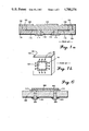
- FIG. 1a, 1b is a sketch of a chip carrier representative of the known state of the art.
- FIG. 2a-2f illustrates a possible process sequence for effecting the embodiment described according to the present invention for processing the ceramic substrate.
- FIG. 3a-3b illustrates a possible process sequence for effecting the embodiment of a flexible dielectric layer by utilizing a secondary process before combining it with the ceramic substrate of the present invention.
- FIG. 4 shows the combination of the ceramic substrate prepared according to the primary process depicted in FIG. 2 and the flexible dielectric layer prepared by the secondary process of FIG. 3 to form the chip carrier arrangement according to the present invention.
- FIG. 5 illustrates a top view of the chip carrier of FIG. 4 with a mounted semiconductor chip connected via bond wires.
- FIG. 6 illustrates another embodiment of the present invention utilizing the ceramic substrate prepared according to the primary process of FIG. 2 and to which is added a flexible dielectric layer utilizing a different secondary process to achieve the same structure and result of the present invention.
- FIG. 1a shows a side view sketch of a chip carrier representative of the known state of the art.
- FIG. 1b shows a perspective top view of the chip carrier arrangement of FIG. 1a and having a semiconductor chip mounted thereon.
- a first ceramic layer 100 consisting of alumina (or A1 2 O 3 ), has a number of through-holes 102 which are punched and then filled with conductive glass-metal paste.
- screened metal pads such as the metal die mount pad 104 and metal wire bond pads 106.
- the metal wire bond pads 106 are aligned to conductively connect with the through-holes 102.
- a second ceramic layer 108 which is typically also made of alumina.
- This ceramic layer 108 also has through-holes 110 which have been provided and filled with conductive glass-metal paste.
- this chip carrier arrangement consists of ceramic layer 100 (having a metal die pad 104 and a plurality of metal wire bond pads 106) bonded to ceramic layer 108. As shown in FIG. 1b, this chip carrier arrangement is ready for mounting a semiconductor chip 120, such as an integrated circuit chip.
- a cover which ordinarily supplied to provide a sealed package, is not shown in order to clarify how the semiconductor chip mounts and interconnects with the chip carrier arrangement.
- the chip carrier arrangement as depicted in FIGS. 1a, 1b is subject to all of the previously enumerated deficiencies set forth with some particularity in the background of the invention. That is, it utilizes expensive co-fired techniques which necessarily limit the minimum possible size of the chip carrier arrangement and which, in turn, affect the reliability as well as the per unit cost.
- FIG. 2 a primary process is shown in FIG. 2 for fabricating a ceramic layer consisting of an alumina substrate 200 drilled to have an array of holes. See step a of FIG. 2. These holes may be of the type formed by known laser-drilling techniques. Proceeding to step b of FIG. 2, a first metallized layer 202 is applied to a surface of the alumina substrate 200 using conventional vacuum metallization techniques. Proceeding to step c of FIG.
- this metallized surface as well as the through-holes is then photodelineated, electroplated with copper, nickel, and gold, and then etched to form individual conductors 204 which remain electrically connected to a respective conductive through-hole.
- step d of FIG. 2 the through holes in the alumina substrate 200 are solder-plugged. This step forms solder plugs 206 which will later serve to provide a hermetic seal as well as the surface mount interconnection points for the final chip carrier arrangement.
- a second metallized layer 208 is added to the alumina substate 200.
- this second metallized layer 208 is similarly photodelineated, electroplated, and etched to form individual conductors 210 which interconnect with solder plugs 206 in the through-holes.
- Step a of FIG. 3 begins with a flexible dielectric film 300 made of a polymer such as a polyimide film, and known as Kapton, a registered trademark of Dupont.
- This flexible dielectric film 300 also has a metallized layer 302.
- this flexible dielectric film 300 processed generally as a large sheet is next subdivided into the required square slips 304, as shown.
- a metallized flexible dielectric polyimide film slip 304 fabricated according to the process of FIG. 3, is attached to the alumina substrate 200 previously fabricated according to the process of FIG. 2.
- the flexible dielectric slip 304 is held in place by means of adhesive 402, which may be an acrylic adhesive.
- adhesive 402 may be an acrylic adhesive.
- the metallized top layer 302 of flexible dielectric slip 304 is ready to have a semiconductor chip affixed.
- FIG. 5 a top perspective view of the chip carrier arrangement disclosed in FIG. 4 shows that bond wires 500 are utilized for interconnecting to a semiconductor chip 502 after it is mounted on metallized dielectric slip 304.
- the preferred embodiment of the present invention provides a chip carrier arrangement having improved reliability directly attributable to a 40 percent size reduction. Moreover, the cost has been reduced by approximately 40 percent, when compared to previously known chip carrier arrangements fabricated using high temperature, co-fired, techniques. These improvements were not previously possible because chip carriers fabricated using high temperature, co-fired techniques could only achieve conductor widths in the range of 5 to 8 mils, whereas the chip carrier arrangement according to the present invention is capable of achieving line widths less than 5 mils.
- the greater precision needed to implement an ultra high density chip carrier is made possible using electroplated, laser-drilled holes plugged with solder which overcome the limitations due to inaccuracies associated with high temperature co-fired fabrication techniques.
- vacuum metallization techniques are used to good advantage at every step to implement narrower conductors which outwardly extend just enough to clear the dielectric layer to be affixed on the surface of the ceramic substrate base: first, depositing metal using known vacuum metallization techniques; next, photodelineating the footprint or conductor pattern; then, electroplating copper, nickel, and gold onto the desired pattern and including the laser-drilled through-holes; and finally, etching away the undesired metal to complete the process.
- the metallized dielectric film also possesses stable material properties which allow it to be advantageously utilized as the dielectric layer. Even in thin sheet form, it provides a material capable of being affixed to ceramic on one surface, and to a metallized layer on its other surface, while still maintaining reasonable dielectric properties.
- FIG. 6 an alternate embodiment of the present invention is shown having a solution coated flexible dielectric film 600 having a metallized top layer 602 which is affixed to the ceramic alumina substrate 200 fabricated according to the primary process steps of FIG. 2, but in which the film 600 is applied directly without the use of an adhesive.
- Both the chip carrier arrangement depicted in FIG. 6 and that depicted in FIG. 4 exhibit good adhesion properties which are attributable to the smooth upper surface of ceramic alumina substrate 200 which is notably not riddled with solder bumps. Another benefit attributable to the structure of FIG. 6 (as well as FIG.
- the present invention not only achieves a smaller, more dense chip carrier arrangement, but also maintains or improves the reliability of the electrical connections made when surface mounting the chip carrier to a board.
- the ultra high density chip carrier arrangement permits the construction of an improved, yet smaller and simplified, chip carrier without the need for expensive, high temperature, co-fired techniques.
- this chip carrier arrangement not only eliminates expensive assembly techniques, but also advantageously utilizes several of the material properties of the flexible dielectric layer in conjunction with known thin-film technques to achieve a smaller, more dense chip carrier, thus overcoming the limitations of the known prior art.
Abstract
Description
Claims (8)
Priority Applications (6)
| Application Number | Priority Date | Filing Date | Title |
|---|---|---|---|
| US06/816,164 US4700276A (en) | 1986-01-03 | 1986-01-03 | Ultra high density pad array chip carrier |
| US06/902,819 US4700473A (en) | 1986-01-03 | 1986-09-02 | Method of making an ultra high density pad array chip carrier |
| KR1019870700800A KR950001181B1 (en) | 1986-01-03 | 1986-12-22 | Ultra high density pad array chip carrier |
| PCT/US1986/002814 WO1987004316A1 (en) | 1986-01-03 | 1986-12-22 | Ultra high density pad array chip carrier |
| JP50111587A JPH081936B2 (en) | 1986-01-03 | 1986-12-22 | Chip carrier and method of manufacturing the same |
| EP19870900987 EP0252977A4 (en) | 1986-01-03 | 1986-12-22 | Ultra high density pad array chip carrier. |
Applications Claiming Priority (1)
| Application Number | Priority Date | Filing Date | Title |
|---|---|---|---|
| US06/816,164 US4700276A (en) | 1986-01-03 | 1986-01-03 | Ultra high density pad array chip carrier |
Related Child Applications (1)
| Application Number | Title | Priority Date | Filing Date |
|---|---|---|---|
| US06/902,819 Division US4700473A (en) | 1986-01-03 | 1986-09-02 | Method of making an ultra high density pad array chip carrier |
Publications (1)
| Publication Number | Publication Date |
|---|---|
| US4700276A true US4700276A (en) | 1987-10-13 |
Family
ID=25219845
Family Applications (1)
| Application Number | Title | Priority Date | Filing Date |
|---|---|---|---|
| US06/816,164 Expired - Fee Related US4700276A (en) | 1986-01-03 | 1986-01-03 | Ultra high density pad array chip carrier |
Country Status (1)
| Country | Link |
|---|---|
| US (1) | US4700276A (en) |
Cited By (55)
| Publication number | Priority date | Publication date | Assignee | Title |
|---|---|---|---|---|
| US5077633A (en) * | 1989-05-01 | 1991-12-31 | Motorola Inc. | Grounding an ultra high density pad array chip carrier |
| US5198887A (en) * | 1991-03-06 | 1993-03-30 | Motorola, Inc. | Semiconductor chip carrier |
| US5241456A (en) * | 1990-07-02 | 1993-08-31 | General Electric Company | Compact high density interconnect structure |
| US5249098A (en) * | 1991-08-22 | 1993-09-28 | Lsi Logic Corporation | Semiconductor device package with solder bump electrical connections on an external surface of the package |
| US5299730A (en) * | 1989-08-28 | 1994-04-05 | Lsi Logic Corporation | Method and apparatus for isolation of flux materials in flip-chip manufacturing |
| US5311060A (en) * | 1989-12-19 | 1994-05-10 | Lsi Logic Corporation | Heat sink for semiconductor device assembly |
| US5321210A (en) * | 1991-01-09 | 1994-06-14 | Nec Corporation | Polyimide multilayer wiring board and method of producing same |
| US5323105A (en) * | 1991-08-08 | 1994-06-21 | International Business Machines Corporation | Test template for monitoring the pins of a multi-pin chip cirucit package |
| US5388327A (en) * | 1993-09-15 | 1995-02-14 | Lsi Logic Corporation | Fabrication of a dissolvable film carrier containing conductive bump contacts for placement on a semiconductor device package |
| US5399903A (en) * | 1990-08-15 | 1995-03-21 | Lsi Logic Corporation | Semiconductor device having an universal die size inner lead layout |
| US5434750A (en) * | 1992-02-07 | 1995-07-18 | Lsi Logic Corporation | Partially-molded, PCB chip carrier package for certain non-square die shapes |
| US5438224A (en) * | 1992-04-23 | 1995-08-01 | Motorola, Inc. | Integrated circuit package having a face-to-face IC chip arrangement |
| US5438477A (en) * | 1993-08-12 | 1995-08-01 | Lsi Logic Corporation | Die-attach technique for flip-chip style mounting of semiconductor dies |
| US5471011A (en) * | 1994-05-26 | 1995-11-28 | Ak Technology, Inc. | Homogeneous thermoplastic semi-conductor chip carrier package |
| US5489804A (en) * | 1989-08-28 | 1996-02-06 | Lsi Logic Corporation | Flexible preformed planar structures for interposing between a chip and a substrate |
| US5504035A (en) * | 1989-08-28 | 1996-04-02 | Lsi Logic Corporation | Process for solder ball interconnecting a semiconductor device to a substrate using a noble metal foil embedded interposer substrate |
| US5650593A (en) * | 1994-05-26 | 1997-07-22 | Amkor Electronics, Inc. | Thermally enhanced chip carrier package |
| US5703405A (en) * | 1993-03-15 | 1997-12-30 | Motorola, Inc. | Integrated circuit chip formed from processing two opposing surfaces of a wafer |
| US5767580A (en) * | 1993-04-30 | 1998-06-16 | Lsi Logic Corporation | Systems having shaped, self-aligning micro-bump structures |
| US5770889A (en) * | 1995-12-29 | 1998-06-23 | Lsi Logic Corporation | Systems having advanced pre-formed planar structures |
| US5820014A (en) | 1993-11-16 | 1998-10-13 | Form Factor, Inc. | Solder preforms |
| US5834799A (en) * | 1989-08-28 | 1998-11-10 | Lsi Logic | Optically transmissive preformed planar structures |
| US5994152A (en) | 1996-02-21 | 1999-11-30 | Formfactor, Inc. | Fabricating interconnects and tips using sacrificial substrates |
| US6096576A (en) * | 1997-09-02 | 2000-08-01 | Silicon Light Machines | Method of producing an electrical interface to an integrated circuit device having high density I/O count |
| US6242302B1 (en) * | 1998-09-03 | 2001-06-05 | Micron Technology, Inc. | Semiconductor processing methods of forming contact openings, methods of forming electrical connections and interconnections, and integrated circuitry |
| US6274823B1 (en) | 1993-11-16 | 2001-08-14 | Formfactor, Inc. | Interconnection substrates with resilient contact structures on both sides |
| US6300578B1 (en) * | 1998-07-01 | 2001-10-09 | International Business Machines Corporation | Pad-on-via assembly technique |
| US6433419B2 (en) | 1990-09-24 | 2002-08-13 | Tessera, Inc. | Face-up semiconductor chip assemblies |
| US20020182903A1 (en) * | 1997-01-30 | 2002-12-05 | Naoto Ishida | Printed wiring board and manufacturing method therefor |
| US20030024114A1 (en) * | 2001-07-14 | 2003-02-06 | Andre Koerner | Method for producing an electrical connection between a plug element and a printed circuit board |
| US6528877B2 (en) | 1999-02-08 | 2003-03-04 | Infineon Technologies Ag | Semiconductor component having a chip carrier with openings for making contact |
| US20040010761A1 (en) * | 2002-07-10 | 2004-01-15 | Alexander Tetelbaum | Integrated circuit design flow with capacitive margin |
| US6707591B2 (en) | 2001-04-10 | 2004-03-16 | Silicon Light Machines | Angled illumination for a single order light modulator based projection system |
| US6714337B1 (en) | 2002-06-28 | 2004-03-30 | Silicon Light Machines | Method and device for modulating a light beam and having an improved gamma response |
| US6712480B1 (en) | 2002-09-27 | 2004-03-30 | Silicon Light Machines | Controlled curvature of stressed micro-structures |
| US6728023B1 (en) | 2002-05-28 | 2004-04-27 | Silicon Light Machines | Optical device arrays with optimized image resolution |
| US6747781B2 (en) | 2001-06-25 | 2004-06-08 | Silicon Light Machines, Inc. | Method, apparatus, and diffuser for reducing laser speckle |
| US6764875B2 (en) | 1998-07-29 | 2004-07-20 | Silicon Light Machines | Method of and apparatus for sealing an hermetic lid to a semiconductor die |
| US6767751B2 (en) | 2002-05-28 | 2004-07-27 | Silicon Light Machines, Inc. | Integrated driver process flow |
| US6782205B2 (en) | 2001-06-25 | 2004-08-24 | Silicon Light Machines | Method and apparatus for dynamic equalization in wavelength division multiplexing |
| US20040188837A1 (en) * | 2003-03-25 | 2004-09-30 | Hyeong-Seob Kim | Wafer level package, multi-package stack, and method of manufacturing the same |
| US6801354B1 (en) | 2002-08-20 | 2004-10-05 | Silicon Light Machines, Inc. | 2-D diffraction grating for substantially eliminating polarization dependent losses |
| US6800238B1 (en) | 2002-01-15 | 2004-10-05 | Silicon Light Machines, Inc. | Method for domain patterning in low coercive field ferroelectrics |
| US6806997B1 (en) | 2003-02-28 | 2004-10-19 | Silicon Light Machines, Inc. | Patterned diffractive light modulator ribbon for PDL reduction |
| US6813059B2 (en) | 2002-06-28 | 2004-11-02 | Silicon Light Machines, Inc. | Reduced formation of asperities in contact micro-structures |
| US6822797B1 (en) | 2002-05-31 | 2004-11-23 | Silicon Light Machines, Inc. | Light modulator structure for producing high-contrast operation using zero-order light |
| US6829258B1 (en) | 2002-06-26 | 2004-12-07 | Silicon Light Machines, Inc. | Rapidly tunable external cavity laser |
| US6829092B2 (en) | 2001-08-15 | 2004-12-07 | Silicon Light Machines, Inc. | Blazed grating light valve |
| US6829077B1 (en) | 2003-02-28 | 2004-12-07 | Silicon Light Machines, Inc. | Diffractive light modulator with dynamically rotatable diffraction plane |
| US7098078B2 (en) | 1990-09-24 | 2006-08-29 | Tessera, Inc. | Microelectronic component and assembly having leads with offset portions |
| US20090205858A1 (en) * | 2006-06-07 | 2009-08-20 | Bernd Haegele | Circuit carrier |
| US8033838B2 (en) | 1996-02-21 | 2011-10-11 | Formfactor, Inc. | Microelectronic contact structure |
| US20180269141A1 (en) * | 2008-05-09 | 2018-09-20 | Invensas Corporation | Chip-size, double side connection package and method for manufacturing the same |
| US11031362B2 (en) | 2017-04-21 | 2021-06-08 | Invensas Corporation | 3D-interconnect |
| US20220122946A1 (en) * | 2020-10-20 | 2022-04-21 | Innolux Corporation | Electronic device |
Citations (13)
| Publication number | Priority date | Publication date | Assignee | Title |
|---|---|---|---|---|
| US3658618A (en) * | 1968-10-25 | 1972-04-25 | Telefunken Patent | Method of providing individual bodies on a basic body |
| US3838984A (en) * | 1973-04-16 | 1974-10-01 | Sperry Rand Corp | Flexible carrier and interconnect for uncased ic chips |
| US3868724A (en) * | 1973-11-21 | 1975-02-25 | Fairchild Camera Instr Co | Multi-layer connecting structures for packaging semiconductor devices mounted on a flexible carrier |
| JPS5230382A (en) * | 1975-09-03 | 1977-03-08 | Nippon Telegr & Teleph Corp <Ntt> | Semiconductor package device |
| DE2657313A1 (en) * | 1976-12-17 | 1978-06-22 | Siemens Ag | Circuit board or contact support - has holes in which component leads or pins are placed and subsequently dip soldered |
| US4202007A (en) * | 1978-06-23 | 1980-05-06 | International Business Machines Corporation | Multi-layer dielectric planar structure having an internal conductor pattern characterized with opposite terminations disposed at a common edge surface of the layers |
| US4251852A (en) * | 1979-06-18 | 1981-02-17 | International Business Machines Corporation | Integrated circuit package |
| US4336551A (en) * | 1977-05-30 | 1982-06-22 | Hitachi, Ltd. | Thick-film printed circuit board and method for producing the same |
| US4381602A (en) * | 1980-12-29 | 1983-05-03 | Honeywell Information Systems Inc. | Method of mounting an I.C. chip on a substrate |
| US4413308A (en) * | 1981-08-31 | 1983-11-01 | Bell Telephone Laboratories, Incorporated | Printed wiring board construction |
| US4437109A (en) * | 1980-11-07 | 1984-03-13 | General Electric Company | Silicon-on-sapphire body with conductive paths therethrough |
| US4446477A (en) * | 1981-08-21 | 1984-05-01 | Sperry Corporation | Multichip thin film module |
| US4509096A (en) * | 1983-02-22 | 1985-04-02 | Smiths Industries Public Limited Company | Chip-carrier substrates |
-
1986
- 1986-01-03 US US06/816,164 patent/US4700276A/en not_active Expired - Fee Related
Patent Citations (13)
| Publication number | Priority date | Publication date | Assignee | Title |
|---|---|---|---|---|
| US3658618A (en) * | 1968-10-25 | 1972-04-25 | Telefunken Patent | Method of providing individual bodies on a basic body |
| US3838984A (en) * | 1973-04-16 | 1974-10-01 | Sperry Rand Corp | Flexible carrier and interconnect for uncased ic chips |
| US3868724A (en) * | 1973-11-21 | 1975-02-25 | Fairchild Camera Instr Co | Multi-layer connecting structures for packaging semiconductor devices mounted on a flexible carrier |
| JPS5230382A (en) * | 1975-09-03 | 1977-03-08 | Nippon Telegr & Teleph Corp <Ntt> | Semiconductor package device |
| DE2657313A1 (en) * | 1976-12-17 | 1978-06-22 | Siemens Ag | Circuit board or contact support - has holes in which component leads or pins are placed and subsequently dip soldered |
| US4336551A (en) * | 1977-05-30 | 1982-06-22 | Hitachi, Ltd. | Thick-film printed circuit board and method for producing the same |
| US4202007A (en) * | 1978-06-23 | 1980-05-06 | International Business Machines Corporation | Multi-layer dielectric planar structure having an internal conductor pattern characterized with opposite terminations disposed at a common edge surface of the layers |
| US4251852A (en) * | 1979-06-18 | 1981-02-17 | International Business Machines Corporation | Integrated circuit package |
| US4437109A (en) * | 1980-11-07 | 1984-03-13 | General Electric Company | Silicon-on-sapphire body with conductive paths therethrough |
| US4381602A (en) * | 1980-12-29 | 1983-05-03 | Honeywell Information Systems Inc. | Method of mounting an I.C. chip on a substrate |
| US4446477A (en) * | 1981-08-21 | 1984-05-01 | Sperry Corporation | Multichip thin film module |
| US4413308A (en) * | 1981-08-31 | 1983-11-01 | Bell Telephone Laboratories, Incorporated | Printed wiring board construction |
| US4509096A (en) * | 1983-02-22 | 1985-04-02 | Smiths Industries Public Limited Company | Chip-carrier substrates |
Non-Patent Citations (4)
| Title |
|---|
| I.E.E.E. Spectrum, Reed Bowlby, Jun. 1985, pp. 37 42, Describes the Evolution of Integrated Circuit Packages from the Mainstay DIP to Newer, More Dense, Chip Carrier Packages, With and Without Leads. * |
| I.E.E.E. Spectrum, Reed Bowlby, Jun. 1985, pp. 37-42, Describes the Evolution of Integrated Circuit Packages from the Mainstay "DIP" to Newer, More Dense, Chip-Carrier Packages, With and Without Leads. |
| Stephans, E., "Pinless Module Connector", IBM Tech. Discl. Bul., vol. 20, No. 10, Mar. 1978, p. 3872. |
| Stephans, E., Pinless Module Connector , IBM Tech. Discl. Bul., vol. 20, No. 10, Mar. 1978, p. 3872. * |
Cited By (77)
| Publication number | Priority date | Publication date | Assignee | Title |
|---|---|---|---|---|
| US5077633A (en) * | 1989-05-01 | 1991-12-31 | Motorola Inc. | Grounding an ultra high density pad array chip carrier |
| US5347162A (en) * | 1989-08-28 | 1994-09-13 | Lsi Logic Corporation | Preformed planar structures employing embedded conductors |
| US5504035A (en) * | 1989-08-28 | 1996-04-02 | Lsi Logic Corporation | Process for solder ball interconnecting a semiconductor device to a substrate using a noble metal foil embedded interposer substrate |
| US5834799A (en) * | 1989-08-28 | 1998-11-10 | Lsi Logic | Optically transmissive preformed planar structures |
| US5410805A (en) * | 1989-08-28 | 1995-05-02 | Lsi Logic Corporation | Method and apparatus for isolation of flux materials in "flip-chip" manufacturing |
| US5299730A (en) * | 1989-08-28 | 1994-04-05 | Lsi Logic Corporation | Method and apparatus for isolation of flux materials in flip-chip manufacturing |
| US5489804A (en) * | 1989-08-28 | 1996-02-06 | Lsi Logic Corporation | Flexible preformed planar structures for interposing between a chip and a substrate |
| US5311060A (en) * | 1989-12-19 | 1994-05-10 | Lsi Logic Corporation | Heat sink for semiconductor device assembly |
| US5241456A (en) * | 1990-07-02 | 1993-08-31 | General Electric Company | Compact high density interconnect structure |
| US5399903A (en) * | 1990-08-15 | 1995-03-21 | Lsi Logic Corporation | Semiconductor device having an universal die size inner lead layout |
| US7098078B2 (en) | 1990-09-24 | 2006-08-29 | Tessera, Inc. | Microelectronic component and assembly having leads with offset portions |
| US6433419B2 (en) | 1990-09-24 | 2002-08-13 | Tessera, Inc. | Face-up semiconductor chip assemblies |
| US7271481B2 (en) | 1990-09-24 | 2007-09-18 | Tessera, Inc. | Microelectronic component and assembly having leads with offset portions |
| US5321210A (en) * | 1991-01-09 | 1994-06-14 | Nec Corporation | Polyimide multilayer wiring board and method of producing same |
| US5426849A (en) * | 1991-01-09 | 1995-06-27 | Nec Corporation | Method of producing a polyimide multilayer wiring board |
| US5198887A (en) * | 1991-03-06 | 1993-03-30 | Motorola, Inc. | Semiconductor chip carrier |
| US5323105A (en) * | 1991-08-08 | 1994-06-21 | International Business Machines Corporation | Test template for monitoring the pins of a multi-pin chip cirucit package |
| US5249098A (en) * | 1991-08-22 | 1993-09-28 | Lsi Logic Corporation | Semiconductor device package with solder bump electrical connections on an external surface of the package |
| US5434750A (en) * | 1992-02-07 | 1995-07-18 | Lsi Logic Corporation | Partially-molded, PCB chip carrier package for certain non-square die shapes |
| US5438224A (en) * | 1992-04-23 | 1995-08-01 | Motorola, Inc. | Integrated circuit package having a face-to-face IC chip arrangement |
| US5703405A (en) * | 1993-03-15 | 1997-12-30 | Motorola, Inc. | Integrated circuit chip formed from processing two opposing surfaces of a wafer |
| US5767580A (en) * | 1993-04-30 | 1998-06-16 | Lsi Logic Corporation | Systems having shaped, self-aligning micro-bump structures |
| US5438477A (en) * | 1993-08-12 | 1995-08-01 | Lsi Logic Corporation | Die-attach technique for flip-chip style mounting of semiconductor dies |
| US5388327A (en) * | 1993-09-15 | 1995-02-14 | Lsi Logic Corporation | Fabrication of a dissolvable film carrier containing conductive bump contacts for placement on a semiconductor device package |
| US5820014A (en) | 1993-11-16 | 1998-10-13 | Form Factor, Inc. | Solder preforms |
| US6274823B1 (en) | 1993-11-16 | 2001-08-14 | Formfactor, Inc. | Interconnection substrates with resilient contact structures on both sides |
| US5650593A (en) * | 1994-05-26 | 1997-07-22 | Amkor Electronics, Inc. | Thermally enhanced chip carrier package |
| US5471011A (en) * | 1994-05-26 | 1995-11-28 | Ak Technology, Inc. | Homogeneous thermoplastic semi-conductor chip carrier package |
| US5770889A (en) * | 1995-12-29 | 1998-06-23 | Lsi Logic Corporation | Systems having advanced pre-formed planar structures |
| US5994152A (en) | 1996-02-21 | 1999-11-30 | Formfactor, Inc. | Fabricating interconnects and tips using sacrificial substrates |
| US8033838B2 (en) | 1996-02-21 | 2011-10-11 | Formfactor, Inc. | Microelectronic contact structure |
| US6784374B2 (en) * | 1997-01-30 | 2004-08-31 | Ibiden Co., Ltd. | Printed wiring board and manufacturing method therefor |
| US20020182903A1 (en) * | 1997-01-30 | 2002-12-05 | Naoto Ishida | Printed wiring board and manufacturing method therefor |
| US6096576A (en) * | 1997-09-02 | 2000-08-01 | Silicon Light Machines | Method of producing an electrical interface to an integrated circuit device having high density I/O count |
| US6452260B1 (en) | 1997-09-02 | 2002-09-17 | Silicon Light Machines | Electrical interface to integrated circuit device having high density I/O count |
| US6300578B1 (en) * | 1998-07-01 | 2001-10-09 | International Business Machines Corporation | Pad-on-via assembly technique |
| US6764875B2 (en) | 1998-07-29 | 2004-07-20 | Silicon Light Machines | Method of and apparatus for sealing an hermetic lid to a semiconductor die |
| US6468883B2 (en) | 1998-09-03 | 2002-10-22 | Micron Technology, Inc. | Semiconductor processing methods of forming contact openings, methods of forming electrical connections and interconnections |
| US20030054621A1 (en) * | 1998-09-03 | 2003-03-20 | Dennison Charles H. | Semiconductor processing methods of forming contact openings, methods of forming electrical connections and interconnections, and integrated circuitry |
| US7291917B2 (en) | 1998-09-03 | 2007-11-06 | Micron Technology, Inc. | Integrated circuitry |
| US6476490B1 (en) | 1998-09-03 | 2002-11-05 | Micron Technology, Inc. | Contact openings, electrical connections and interconnections for integrated circuitry |
| US20060273459A1 (en) * | 1998-09-03 | 2006-12-07 | Dennison Charles H | Semiconductor processing methods of forming contact openings, methods of forming electrical connections and interconnections, and integrated circuitry |
| US6242302B1 (en) * | 1998-09-03 | 2001-06-05 | Micron Technology, Inc. | Semiconductor processing methods of forming contact openings, methods of forming electrical connections and interconnections, and integrated circuitry |
| US20060014379A1 (en) * | 1998-09-03 | 2006-01-19 | Dennison Charles H | Semiconductor processing methods of forming contact openings, methods of forming electrical connections and interconnections, and integrated circuitry |
| US6855628B2 (en) | 1998-09-03 | 2005-02-15 | Micron Technology, Inc. | Semiconductor processing methods of forming contact openings, methods of forming electrical connections and interconnections, and integrated circuitry |
| US6753241B2 (en) | 1998-09-03 | 2004-06-22 | Micron Technology, Inc. | Semiconductor processing methods of forming contact openings, methods of forming electrical connections and interconnections, and integrated circuitry |
| US6323087B1 (en) * | 1998-09-03 | 2001-11-27 | Micron Technology, Inc. | Semiconductor processing methods of forming contact openings, methods of forming electrical connections and interconnections, and integrated circuitry |
| US6528877B2 (en) | 1999-02-08 | 2003-03-04 | Infineon Technologies Ag | Semiconductor component having a chip carrier with openings for making contact |
| US6707591B2 (en) | 2001-04-10 | 2004-03-16 | Silicon Light Machines | Angled illumination for a single order light modulator based projection system |
| US6782205B2 (en) | 2001-06-25 | 2004-08-24 | Silicon Light Machines | Method and apparatus for dynamic equalization in wavelength division multiplexing |
| US6747781B2 (en) | 2001-06-25 | 2004-06-08 | Silicon Light Machines, Inc. | Method, apparatus, and diffuser for reducing laser speckle |
| US20030024114A1 (en) * | 2001-07-14 | 2003-02-06 | Andre Koerner | Method for producing an electrical connection between a plug element and a printed circuit board |
| US6898847B2 (en) * | 2001-07-14 | 2005-05-31 | Hella Kg Hueck & Co. | Method for producing an electrical connection between a plug element and a printed circuit board |
| US6829092B2 (en) | 2001-08-15 | 2004-12-07 | Silicon Light Machines, Inc. | Blazed grating light valve |
| US6800238B1 (en) | 2002-01-15 | 2004-10-05 | Silicon Light Machines, Inc. | Method for domain patterning in low coercive field ferroelectrics |
| US6767751B2 (en) | 2002-05-28 | 2004-07-27 | Silicon Light Machines, Inc. | Integrated driver process flow |
| US6728023B1 (en) | 2002-05-28 | 2004-04-27 | Silicon Light Machines | Optical device arrays with optimized image resolution |
| US6822797B1 (en) | 2002-05-31 | 2004-11-23 | Silicon Light Machines, Inc. | Light modulator structure for producing high-contrast operation using zero-order light |
| US6829258B1 (en) | 2002-06-26 | 2004-12-07 | Silicon Light Machines, Inc. | Rapidly tunable external cavity laser |
| US6813059B2 (en) | 2002-06-28 | 2004-11-02 | Silicon Light Machines, Inc. | Reduced formation of asperities in contact micro-structures |
| US6714337B1 (en) | 2002-06-28 | 2004-03-30 | Silicon Light Machines | Method and device for modulating a light beam and having an improved gamma response |
| US20040010761A1 (en) * | 2002-07-10 | 2004-01-15 | Alexander Tetelbaum | Integrated circuit design flow with capacitive margin |
| US6801354B1 (en) | 2002-08-20 | 2004-10-05 | Silicon Light Machines, Inc. | 2-D diffraction grating for substantially eliminating polarization dependent losses |
| US6712480B1 (en) | 2002-09-27 | 2004-03-30 | Silicon Light Machines | Controlled curvature of stressed micro-structures |
| US6806997B1 (en) | 2003-02-28 | 2004-10-19 | Silicon Light Machines, Inc. | Patterned diffractive light modulator ribbon for PDL reduction |
| US6829077B1 (en) | 2003-02-28 | 2004-12-07 | Silicon Light Machines, Inc. | Diffractive light modulator with dynamically rotatable diffraction plane |
| US20060033212A1 (en) * | 2003-03-25 | 2006-02-16 | Hyeong-Seob Kim | Wafer level package, multi-package stack, and method of manufacturing the same |
| US6982487B2 (en) * | 2003-03-25 | 2006-01-03 | Samsung Electronics Co., Ltd. | Wafer level package and multi-package stack |
| US7335592B2 (en) * | 2003-03-25 | 2008-02-26 | Samsung Electronics Co., Ltd. | Wafer level package, multi-package stack, and method of manufacturing the same |
| US20040188837A1 (en) * | 2003-03-25 | 2004-09-30 | Hyeong-Seob Kim | Wafer level package, multi-package stack, and method of manufacturing the same |
| US20090205858A1 (en) * | 2006-06-07 | 2009-08-20 | Bernd Haegele | Circuit carrier |
| US8134083B2 (en) * | 2006-06-07 | 2012-03-13 | Ab Mikroelektronik Gesselschaft Mit Beschrankter Haftung | Circuit carrier |
| US20180269141A1 (en) * | 2008-05-09 | 2018-09-20 | Invensas Corporation | Chip-size, double side connection package and method for manufacturing the same |
| US10748840B2 (en) * | 2008-05-09 | 2020-08-18 | Invensas Corporation | Chip-size, double side connection package and method for manufacturing the same |
| US11031362B2 (en) | 2017-04-21 | 2021-06-08 | Invensas Corporation | 3D-interconnect |
| US11929337B2 (en) | 2017-04-21 | 2024-03-12 | Invensas Llc | 3D-interconnect |
| US20220122946A1 (en) * | 2020-10-20 | 2022-04-21 | Innolux Corporation | Electronic device |
Similar Documents
| Publication | Publication Date | Title |
|---|---|---|
| US4700276A (en) | Ultra high density pad array chip carrier | |
| US4700473A (en) | Method of making an ultra high density pad array chip carrier | |
| US5006673A (en) | Fabrication of pad array carriers from a universal interconnect structure | |
| US5386341A (en) | Flexible substrate folded in a U-shape with a rigidizer plate located in the notch of the U-shape | |
| US5289346A (en) | Peripheral to area adapter with protective bumper for an integrated circuit chip | |
| US4763188A (en) | Packaging system for multiple semiconductor devices | |
| US4791075A (en) | Process for making a hermetic low cost pin grid array package | |
| US5379191A (en) | Compact adapter package providing peripheral to area translation for an integrated circuit chip | |
| KR100343386B1 (en) | Thermoelectric module with improved heat-transfer efficiency and method of manufacturing the same | |
| US5069626A (en) | Plated plastic castellated interconnect for electrical components | |
| US5521435A (en) | Semiconductor device and a fabrication process thereof | |
| US4750089A (en) | Circuit board with a chip carrier and mounting structure connected to the chip carrier | |
| CA1142260A (en) | Double cavity semiconductor chip carrier | |
| EP1005086B1 (en) | Metal foil having bumps, circuit substrate having the metal foil, and semiconductor device having the circuit substrate | |
| US4890194A (en) | A chip carrier and mounting structure connected to the chip carrier | |
| EP0072673A2 (en) | Area tape for the electrical interconnection between electronic components and external circuitry | |
| US4688150A (en) | High pin count chip carrier package | |
| JP3113005B2 (en) | Integrated circuit package without carrier | |
| JP3660663B2 (en) | Chip package manufacturing method | |
| US5262674A (en) | Chip carrier for an integrated circuit assembly | |
| US6351389B1 (en) | Device and method for packaging an electronic device | |
| WO1989000346A1 (en) | Plated plastic castellated interconnect for electrical components | |
| JPH09312355A (en) | Semiconductor device and its manufacture | |
| US6444494B1 (en) | Process of packaging a semiconductor device with reinforced film substrate | |
| JP2003273281A (en) | Chip package and its manufacturing method |
Legal Events
| Date | Code | Title | Description |
|---|---|---|---|
| AS | Assignment |
Owner name: MOTOROLA, INC., SCHAUMBURG, ILLINOIS, A CORP OF DE Free format text: ASSIGNMENT OF ASSIGNORS INTEREST.;ASSIGNORS:FREYMAN, BRUCE J.;DORINSKI, DALE;SCHURBOFF, JOHN;REEL/FRAME:004502/0505 Effective date: 19851216 |
|
| FPAY | Fee payment |
Year of fee payment: 4 |
|
| SULP | Surcharge for late payment | ||
| FEPP | Fee payment procedure |
Free format text: PAYOR NUMBER ASSIGNED (ORIGINAL EVENT CODE: ASPN); ENTITY STATUS OF PATENT OWNER: LARGE ENTITY |
|
| FPAY | Fee payment |
Year of fee payment: 8 |
|
| REMI | Maintenance fee reminder mailed | ||
| LAPS | Lapse for failure to pay maintenance fees | ||
| FP | Lapsed due to failure to pay maintenance fee |
Effective date: 19991013 |
|
| STCH | Information on status: patent discontinuation |
Free format text: PATENT EXPIRED DUE TO NONPAYMENT OF MAINTENANCE FEES UNDER 37 CFR 1.362 |