US20040264236A1 - Nonvolatile semiconductor memory device having a gate stack and method of manufacturing the same - Google Patents
Nonvolatile semiconductor memory device having a gate stack and method of manufacturing the same Download PDFInfo
- Publication number
- US20040264236A1 US20040264236A1 US10/835,097 US83509704A US2004264236A1 US 20040264236 A1 US20040264236 A1 US 20040264236A1 US 83509704 A US83509704 A US 83509704A US 2004264236 A1 US2004264236 A1 US 2004264236A1
- Authority
- US
- United States
- Prior art keywords
- film
- trapping material
- oxide film
- memory device
- semiconductor memory
- Prior art date
- Legal status (The legal status is an assumption and is not a legal conclusion. Google has not performed a legal analysis and makes no representation as to the accuracy of the status listed.)
- Granted
Links
- 239000004065 semiconductor Substances 0.000 title claims abstract description 84
- 238000004519 manufacturing process Methods 0.000 title claims description 11
- 239000000463 material Substances 0.000 claims abstract description 133
- 230000005641 tunneling Effects 0.000 claims abstract description 65
- 150000004767 nitrides Chemical class 0.000 claims abstract description 34
- 239000000758 substrate Substances 0.000 claims abstract description 30
- 239000012535 impurity Substances 0.000 claims abstract description 23
- 229910052581 Si3N4 Inorganic materials 0.000 claims abstract description 9
- TWNQGVIAIRXVLR-UHFFFAOYSA-N oxo(oxoalumanyloxy)alumane Chemical compound O=[Al]O[Al]=O TWNQGVIAIRXVLR-UHFFFAOYSA-N 0.000 claims description 49
- MCMNRKCIXSYSNV-UHFFFAOYSA-N ZrO2 Inorganic materials O=[Zr]=O MCMNRKCIXSYSNV-UHFFFAOYSA-N 0.000 claims description 43
- GWEVSGVZZGPLCZ-UHFFFAOYSA-N titanium dioxide Inorganic materials O=[Ti]=O GWEVSGVZZGPLCZ-UHFFFAOYSA-N 0.000 claims description 43
- CJNBYAVZURUTKZ-UHFFFAOYSA-N hafnium(IV) oxide Inorganic materials O=[Hf]=O CJNBYAVZURUTKZ-UHFFFAOYSA-N 0.000 claims description 26
- PBCFLUZVCVVTBY-UHFFFAOYSA-N tantalum pentoxide Inorganic materials O=[Ta](=O)O[Ta](=O)=O PBCFLUZVCVVTBY-UHFFFAOYSA-N 0.000 claims description 22
- 229910052747 lanthanoid Inorganic materials 0.000 claims description 19
- 150000002602 lanthanoids Chemical class 0.000 claims description 19
- 238000000034 method Methods 0.000 claims description 17
- 238000003949 trap density measurement Methods 0.000 abstract description 7
- VYPSYNLAJGMNEJ-UHFFFAOYSA-N Silicium dioxide Chemical compound O=[Si]=O VYPSYNLAJGMNEJ-UHFFFAOYSA-N 0.000 description 40
- 229910052814 silicon oxide Inorganic materials 0.000 description 40
- 230000005684 electric field Effects 0.000 description 25
- 230000014759 maintenance of location Effects 0.000 description 11
- 230000004888 barrier function Effects 0.000 description 10
- 238000009792 diffusion process Methods 0.000 description 7
- 229910000449 hafnium oxide Inorganic materials 0.000 description 5
- WIHZLLGSGQNAGK-UHFFFAOYSA-N hafnium(4+);oxygen(2-) Chemical compound [O-2].[O-2].[Hf+4] WIHZLLGSGQNAGK-UHFFFAOYSA-N 0.000 description 5
- 238000009826 distribution Methods 0.000 description 4
- 229910052692 Dysprosium Inorganic materials 0.000 description 3
- 229940037003 alum Drugs 0.000 description 3
- 238000000231 atomic layer deposition Methods 0.000 description 3
- 229910052735 hafnium Inorganic materials 0.000 description 3
- HQVNEWCFYHHQES-UHFFFAOYSA-N silicon nitride Chemical compound N12[Si]34N5[Si]62N3[Si]51N64 HQVNEWCFYHHQES-UHFFFAOYSA-N 0.000 description 3
- 229910052684 Cerium Inorganic materials 0.000 description 2
- 229910052691 Erbium Inorganic materials 0.000 description 2
- 229910052693 Europium Inorganic materials 0.000 description 2
- 229910052688 Gadolinium Inorganic materials 0.000 description 2
- 229910052689 Holmium Inorganic materials 0.000 description 2
- 229910052765 Lutetium Inorganic materials 0.000 description 2
- 229910052779 Neodymium Inorganic materials 0.000 description 2
- 229910052777 Praseodymium Inorganic materials 0.000 description 2
- 229910052772 Samarium Inorganic materials 0.000 description 2
- 229910052771 Terbium Inorganic materials 0.000 description 2
- 229910052775 Thulium Inorganic materials 0.000 description 2
- 229910052769 Ytterbium Inorganic materials 0.000 description 2
- 238000005229 chemical vapour deposition Methods 0.000 description 2
- 238000000151 deposition Methods 0.000 description 2
- 239000002019 doping agent Substances 0.000 description 2
- 238000005530 etching Methods 0.000 description 2
- 238000002474 experimental method Methods 0.000 description 2
- 239000011810 insulating material Substances 0.000 description 2
- 229910052746 lanthanum Inorganic materials 0.000 description 2
- 238000000682 scanning probe acoustic microscopy Methods 0.000 description 2
- 229910052710 silicon Inorganic materials 0.000 description 2
- 239000010703 silicon Substances 0.000 description 2
- 230000000903 blocking effect Effects 0.000 description 1
- 238000013500 data storage Methods 0.000 description 1
- 230000007423 decrease Effects 0.000 description 1
- 238000011161 development Methods 0.000 description 1
- 230000018109 developmental process Effects 0.000 description 1
- KBQHZAAAGSGFKK-UHFFFAOYSA-N dysprosium atom Chemical compound [Dy] KBQHZAAAGSGFKK-UHFFFAOYSA-N 0.000 description 1
- 230000000694 effects Effects 0.000 description 1
- VBJZVLUMGGDVMO-UHFFFAOYSA-N hafnium atom Chemical compound [Hf] VBJZVLUMGGDVMO-UHFFFAOYSA-N 0.000 description 1
- 238000010438 heat treatment Methods 0.000 description 1
- 238000005468 ion implantation Methods 0.000 description 1
- 238000005259 measurement Methods 0.000 description 1
- 229910021420 polycrystalline silicon Inorganic materials 0.000 description 1
- 229920005591 polysilicon Polymers 0.000 description 1
- 230000000717 retained effect Effects 0.000 description 1
- 239000007787 solid Substances 0.000 description 1
- 238000004544 sputter deposition Methods 0.000 description 1
- 238000003860 storage Methods 0.000 description 1
- WQJQOUPTWCFRMM-UHFFFAOYSA-N tungsten disilicide Chemical compound [Si]#[W]#[Si] WQJQOUPTWCFRMM-UHFFFAOYSA-N 0.000 description 1
- 229910021342 tungsten silicide Inorganic materials 0.000 description 1
Images


Classifications
-
- H—ELECTRICITY
- H10—SEMICONDUCTOR DEVICES; ELECTRIC SOLID-STATE DEVICES NOT OTHERWISE PROVIDED FOR
- H10B—ELECTRONIC MEMORY DEVICES
- H10B99/00—Subject matter not provided for in other groups of this subclass
-
- H—ELECTRICITY
- H01—ELECTRIC ELEMENTS
- H01L—SEMICONDUCTOR DEVICES NOT COVERED BY CLASS H10
- H01L29/00—Semiconductor devices adapted for rectifying, amplifying, oscillating or switching, or capacitors or resistors with at least one potential-jump barrier or surface barrier, e.g. PN junction depletion layer or carrier concentration layer; Details of semiconductor bodies or of electrodes thereof ; Multistep manufacturing processes therefor
- H01L29/66—Types of semiconductor device ; Multistep manufacturing processes therefor
- H01L29/68—Types of semiconductor device ; Multistep manufacturing processes therefor controllable by only the electric current supplied, or only the electric potential applied, to an electrode which does not carry the current to be rectified, amplified or switched
- H01L29/76—Unipolar devices, e.g. field effect transistors
- H01L29/772—Field effect transistors
- H01L29/78—Field effect transistors with field effect produced by an insulated gate
- H01L29/792—Field effect transistors with field effect produced by an insulated gate with charge trapping gate insulator, e.g. MNOS-memory transistors
-
- H—ELECTRICITY
- H01—ELECTRIC ELEMENTS
- H01L—SEMICONDUCTOR DEVICES NOT COVERED BY CLASS H10
- H01L21/00—Processes or apparatus adapted for the manufacture or treatment of semiconductor or solid state devices or of parts thereof
- H01L21/02—Manufacture or treatment of semiconductor devices or of parts thereof
- H01L21/04—Manufacture or treatment of semiconductor devices or of parts thereof the devices having at least one potential-jump barrier or surface barrier, e.g. PN junction, depletion layer or carrier concentration layer
- H01L21/18—Manufacture or treatment of semiconductor devices or of parts thereof the devices having at least one potential-jump barrier or surface barrier, e.g. PN junction, depletion layer or carrier concentration layer the devices having semiconductor bodies comprising elements of Group IV of the Periodic System or AIIIBV compounds with or without impurities, e.g. doping materials
- H01L21/28—Manufacture of electrodes on semiconductor bodies using processes or apparatus not provided for in groups H01L21/20 - H01L21/268
- H01L21/28008—Making conductor-insulator-semiconductor electrodes
- H01L21/28017—Making conductor-insulator-semiconductor electrodes the insulator being formed after the semiconductor body, the semiconductor being silicon
- H01L21/28158—Making the insulator
- H01L21/28167—Making the insulator on single crystalline silicon, e.g. using a liquid, i.e. chemical oxidation
- H01L21/28194—Making the insulator on single crystalline silicon, e.g. using a liquid, i.e. chemical oxidation by deposition, e.g. evaporation, ALD, CVD, sputtering, laser deposition
-
- H—ELECTRICITY
- H01—ELECTRIC ELEMENTS
- H01L—SEMICONDUCTOR DEVICES NOT COVERED BY CLASS H10
- H01L29/00—Semiconductor devices adapted for rectifying, amplifying, oscillating or switching, or capacitors or resistors with at least one potential-jump barrier or surface barrier, e.g. PN junction depletion layer or carrier concentration layer; Details of semiconductor bodies or of electrodes thereof ; Multistep manufacturing processes therefor
- H01L29/40—Electrodes ; Multistep manufacturing processes therefor
- H01L29/401—Multistep manufacturing processes
- H01L29/4011—Multistep manufacturing processes for data storage electrodes
- H01L29/40117—Multistep manufacturing processes for data storage electrodes the electrodes comprising a charge-trapping insulator
-
- H—ELECTRICITY
- H01—ELECTRIC ELEMENTS
- H01L—SEMICONDUCTOR DEVICES NOT COVERED BY CLASS H10
- H01L29/00—Semiconductor devices adapted for rectifying, amplifying, oscillating or switching, or capacitors or resistors with at least one potential-jump barrier or surface barrier, e.g. PN junction depletion layer or carrier concentration layer; Details of semiconductor bodies or of electrodes thereof ; Multistep manufacturing processes therefor
- H01L29/40—Electrodes ; Multistep manufacturing processes therefor
- H01L29/43—Electrodes ; Multistep manufacturing processes therefor characterised by the materials of which they are formed
- H01L29/49—Metal-insulator-semiconductor electrodes, e.g. gates of MOSFET
- H01L29/51—Insulating materials associated therewith
- H01L29/511—Insulating materials associated therewith with a compositional variation, e.g. multilayer structures
- H01L29/513—Insulating materials associated therewith with a compositional variation, e.g. multilayer structures the variation being perpendicular to the channel plane
-
- H—ELECTRICITY
- H01—ELECTRIC ELEMENTS
- H01L—SEMICONDUCTOR DEVICES NOT COVERED BY CLASS H10
- H01L29/00—Semiconductor devices adapted for rectifying, amplifying, oscillating or switching, or capacitors or resistors with at least one potential-jump barrier or surface barrier, e.g. PN junction depletion layer or carrier concentration layer; Details of semiconductor bodies or of electrodes thereof ; Multistep manufacturing processes therefor
- H01L29/40—Electrodes ; Multistep manufacturing processes therefor
- H01L29/43—Electrodes ; Multistep manufacturing processes therefor characterised by the materials of which they are formed
- H01L29/49—Metal-insulator-semiconductor electrodes, e.g. gates of MOSFET
- H01L29/51—Insulating materials associated therewith
- H01L29/517—Insulating materials associated therewith the insulating material comprising a metallic compound, e.g. metal oxide, metal silicate
-
- H—ELECTRICITY
- H01—ELECTRIC ELEMENTS
- H01L—SEMICONDUCTOR DEVICES NOT COVERED BY CLASS H10
- H01L29/00—Semiconductor devices adapted for rectifying, amplifying, oscillating or switching, or capacitors or resistors with at least one potential-jump barrier or surface barrier, e.g. PN junction depletion layer or carrier concentration layer; Details of semiconductor bodies or of electrodes thereof ; Multistep manufacturing processes therefor
- H01L29/40—Electrodes ; Multistep manufacturing processes therefor
- H01L29/43—Electrodes ; Multistep manufacturing processes therefor characterised by the materials of which they are formed
- H01L29/49—Metal-insulator-semiconductor electrodes, e.g. gates of MOSFET
- H01L29/51—Insulating materials associated therewith
- H01L29/518—Insulating materials associated therewith the insulating material containing nitrogen, e.g. nitride, oxynitride, nitrogen-doped material
-
- H—ELECTRICITY
- H01—ELECTRIC ELEMENTS
- H01L—SEMICONDUCTOR DEVICES NOT COVERED BY CLASS H10
- H01L29/00—Semiconductor devices adapted for rectifying, amplifying, oscillating or switching, or capacitors or resistors with at least one potential-jump barrier or surface barrier, e.g. PN junction depletion layer or carrier concentration layer; Details of semiconductor bodies or of electrodes thereof ; Multistep manufacturing processes therefor
- H01L29/66—Types of semiconductor device ; Multistep manufacturing processes therefor
- H01L29/66007—Multistep manufacturing processes
- H01L29/66075—Multistep manufacturing processes of devices having semiconductor bodies comprising group 14 or group 13/15 materials
- H01L29/66227—Multistep manufacturing processes of devices having semiconductor bodies comprising group 14 or group 13/15 materials the devices being controllable only by the electric current supplied or the electric potential applied, to an electrode which does not carry the current to be rectified, amplified or switched, e.g. three-terminal devices
- H01L29/66409—Unipolar field-effect transistors
- H01L29/66477—Unipolar field-effect transistors with an insulated gate, i.e. MISFET
- H01L29/66833—Unipolar field-effect transistors with an insulated gate, i.e. MISFET with a charge trapping gate insulator, e.g. MNOS transistors
-
- H—ELECTRICITY
- H10—SEMICONDUCTOR DEVICES; ELECTRIC SOLID-STATE DEVICES NOT OTHERWISE PROVIDED FOR
- H10B—ELECTRONIC MEMORY DEVICES
- H10B43/00—EEPROM devices comprising charge-trapping gate insulators
- H10B43/30—EEPROM devices comprising charge-trapping gate insulators characterised by the memory core region
Definitions
- the present invention relates to a semiconductor memory device. More particularly, the present invention relates to a nonvolatile semiconductor memory device having a gate with a different film structure from a silicon-oxide/nitride/oxide-silicon (SONOS), and a method of manufacturing the same.
- SONOS silicon-oxide/nitride/oxide-silicon
- flash memory device i.e., a special type of an electrically erasable programmable read-only memory (EEPROM), which can be erased or programmed in blocks of data and the contents of which are retained even when the power is turned off.
- the flash memory device generally has a multi-layer structure including a floating gate, where a charge is stored, a transistor gate, where data are stored, and a control gate that controls the floating gate, the gates being sequentially deposited.
- the flash memory has a low retention characteristic and data stored therein cannot be kept safely for a long period of time due to a leakage current.
- FIG. 1 illustrates a cross-section of a basic structure of a conventional SONOS memory device.
- a first silicon oxide (SiO 2 ) film 12 is formed on a channel region between a source region S and drain region D of a substrate 10 .
- One end of the first silicon oxide film 12 contacts the source region S and another end of the first silicon oxide film 12 contacts the drain region D.
- the first silicon oxide film 12 is for tunneling a charge.
- a nitride (Si 3 N 4 ) film 14 is formed on the first silicon oxide film 12 .
- the nitride film 14 which is practically a material film for storing data, traps the charge tunneled through the first silicon oxide film 12 .
- a second silicon oxide film 16 is formed as a barrier film for blocking the movement of the charge from the nitride film 14 upward through the nitride film 14 .
- a gate electrode 18 is formed on the second silicon oxide film 16 .
- an operating voltage of the conventional SONOS device is very high. If a low operating voltage is applied to the conventional SONOS device, the speed of writing/erasing of data becomes much slower than a desired speed. Due to such voltage dependence characteristic, the control of a trap density of the nitride film 14 also becomes difficult. The retention time also is not sufficiently long.
- the present invention is therefore directed to a semiconductor memory device and method of manufacturing the same, which substantially overcomes one or more of the problems due to the limitations and disadvantages of the related art.
- the nonvolatile semiconductor memory device may further include at least one of a first oxide film between the tunneling film and the first trapping material film and a second oxide film between the first trapping material film and the first insulating film. At least one of the first oxide film and the second oxide film may be an aluminum oxide (Al 2 O 3 ) film.
- the nonvolatile semiconductor memory device may further include a second trapping material film doped with a second predetermined impurity, the second trapping material film having a higher dielectric constant than the nitride film, and a second insulating film having a higher dielectric constant than the nitride film, the second trapping material film and the second insulating film being sequentially formed between the first insulating film and the gate electrode.
- the nonvolatile semiconductor memory device may further include at least one, two or three, or all of a first oxide film between the tunneling film and the first trapping material film, a second oxide film between the first trapping material film and the first insulating film, a third oxide film between the first insulating film and the second trapping material film, and a fourth oxide film between the second trapping material film and the second insulating film.
- At least one of the first oxide film, the second oxide film, the third oxide film and the fourth oxide film may be an aluminum oxide film.
- the second trapping material film may be formed of a material selected from the group consisting of HfO 2 , ZrO 2 , Ta 2 O 5 , TiO 2 , and Al 2 O 3 .
- the second insulating film may be a film selected from the group consisting of HfO 2 film, ZrO 2 film, Ta 2 O 5 film, TiO 2 film, and Al 2 O 3 film.
- the first insulating film is a film selected from the group consisting of HfO 2 film, ZrO 2 film, Ta 2 O 5 film, and TiO 2 film.
- the first predetermined impurity may be a lanthanide and may be at a doping concentration of approximately 1 ⁇ 20%.
- the second predetermined impurity may be a lanthanide and may be at a doping concentration of approximately 1-20%.
- a method of manufacturing a nonvolatile semiconductor memory device including forming a tunneling oxide film, forming a first trapping material film doped with a first predetermined impurity, the first trapping material film having a higher dielectric constant than that of a nitride film (Si 3 N 4 ), forming a first insulating film having a higher dielectric constant than that of the nitride film, and forming a gate electrode, wherein the tunneling oxide film, the first trapping material film, the first insulating film, and the gate electrode are sequentially deposited on a semiconductor substrate.
- a gate region is defined on the gate electrode.
- a gate stack is formed by removing the gate electrode, the first insulating film, the first trapping material film, and the tunneling oxide film outside the gate region.
- a source and drain region are formed around the gate stack on the semiconductor substrate.
- the method may further include forming an oxide film on at least one of the tunneling oxide, the first trapping material film, the first insulating layer and the second trapping material film.
- the first trapping material film may be a film selected from the group consisting of HfO 2 film, ZrO 2 film, Ta 2 O 5 film, TiO 2 film and Al 2 O 3 film.
- the first insulating film may be a film selected from the group consisting of HfO 2 film, ZrO 2 film, Ta 2 O 5 film, and TiO 2 film.
- the oxide film may be an aluminum oxide film.
- the second trapping material film may be a film selected from the group consisting of HfO 2 film, ZrO 2 film, Ta 2 O 5 film, TiO 2 film, and Al 2 O 3 film.
- the second insulating film may be a film selected from the group consisting of HfO 2 film, ZrO 2 film, Ta 2 O 5 film, and TiO 2 film.
- the first predetermined impurity may be a lanthanide at a doping concentration of approximately 1 ⁇ 20%.
- a nonvolatile memory device provides the capability of controlling trap density effectively according to the doping concentration. Accordingly, writing/erasing of data can be operated at a lower voltage than in the conventional art, thereby increasing the operating speed as compared to the conventional art.
- FIG. 1 illustrates a cross-section of a conventional SONOS memory device as an example of a conventional nonvolatile memory device
- FIGS. 2 through 5 illustrate cross-sections of nonvolatile memory devices, according to first through fourth embodiments of the present invention
- FIG. 6 is a graph showing the characteristics of a leakage current according to a doping concentration of an insulating film having a high dielectric constant, used for a nonvolatile memory device according to an embodiment of the present invention
- FIG. 7 is a graph showing a variation of a leakage current and an effective thickness according to a doping concentration of an insulating layer having a high conductivity, used for a nonvolatile memory device, according to an embodiment of the present invention
- FIG. 8 is a graph showing a variation of a flat band voltage according to a stress charge, according to an embodiment of the present invention.
- FIG. 9 is a graph showing a variation of a flat band voltage according to a write/read time, according to an embodiment of the present invention.
- FIG. 10 is a graph showing a variation of a flat band voltage according to a retention time, according to an embodiment of the present invention.
- FIG. 11 is a graph showing a variation of a flat band voltage according to a programming time, according to an embodiment of the present invention.
- FIG. 12 is a graph showing a variation of a flat band voltage according to a erasing time, according to an embodiment of the present invention.
- FIG. 13 is a graph showing an energy band of an OHA film according to an embodiment of the present invention and an energy band of an ONO film according to the conventional nonvolatile memory device.
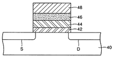
- a source region S and drain region D are formed on a substrate 40 and separated by a predetermined distance.
- a space between the source region S and the drain region D on the substrate 10 defines a channel region.
- a gate stack is formed on the channel region.
- the gate stack is formed of the following layers deposited sequentially.
- a tunneling oxide film 42 is provided on the channel region. One end of the tunneling oxide film 42 contacts the source region S and another end of the tunneling oxide film 42 contacts the drain region D.
- a first trapping material layer 44 is formed on the tunneling oxide film 42 .
- a first insulating film 46 having a high dielectric constant is formed on the first trapping material layer 44 .
- a gate electrode 48 is formed on the first insulating film 46 .
- the first trapping material film 44 traps a charge, i.e., electrons, which pass through the tunneling oxide film 42 .
- the tunneling oxide film 42 may be a silicon oxide film.
- the thickness of the tunneling oxide film 42 may be approximately 1.5 ⁇ 4 nm.
- the first trapping material film 44 may be a non-nitride film or an insulating film doped with a predetermined impurity and having a high dielectric constant.
- the insulating film for the first trapping material film 44 may be an oxide film having a high dielectric constant selected from the group consisting of HfO 2 , ZrO 2 , Ta 2 O 5 , TiO 2 , and Al 2 O 3 .
- a thickness thereof may be approximately 2 ⁇ 15 nm.
- the dopant in the insulating film for the first trapping material film 44 may be a lanthanide, i.e., selected from the group consisting of La, Ce, Pr, Nd, Sm, Eu, Gd, Tb, Dy, Ho, Er, Tm, Yb, and Lu.
- a doping concentration may be approximately 1 ⁇ 20%, e.g., 10%.
- the first insulating film 46 which has a high dielectric constant is formed to prevent a portion of the electrons from moving through the first trapping material film 44 to the gate electrode 48 while the charge is being trapped by the first trapping material film 44 .
- the first insulating film 46 may be formed of an aluminum oxide (Al 2 O 3 ). Other materials having the same or a higher dielectric constant as aluminum oxide may be used for the first insulating film 46 .
- the gate electrode 48 may be formed of a polysilicon electrode doped with a conductive impurity. Alternatively, other electrodes, such as a tungsten silicide electrode, may be used for the gate electrode 48 .
- the second embodiment is related to a nonvolatile semiconductor memory device having a diffusion barrier layer on and under the first trapping material film 44 .
- a second oxide film 52 serving as a second diffusion barrier layer, is formed between the first trapping material film 44 and the first insulating film 46 .
- the second oxide film 52 may be an aluminum oxide film
- the first insulating film 46 may be an insulating film having a high dielectric constant, for example, selected from the group consisting of HfO 2 , ZrO 2 , Ta 2 O 5 , and TiO 2 .
- the thickness of the second oxide film 52 may be approximately 0.5 ⁇ 2 nm, and the thickness of the first insulating film 46 may be approximately 3 ⁇ 20 nm.
- the nonvolatile semiconductor memory device includes an oxide film formed between the first insulating film 46 and the gate electrode 48 and/or between the tunneling oxide film 42 and the first trapping material film 44 .
- the first and second oxide films 50 and 52 may both be aluminum oxide films.
- any material that can act as a diffusion barrier layer can replace the first oxide film 50 and/or the second oxide film 52 .
- any material that can act as a diffusion barrier layer can replace other insulating films other than the oxide film.
- the third embodiment is related to a nonvolatile semiconductor memory device including a gate stack formed on a channel region of a substrate 40 and having a plurality of trapping material films.
- the first trapping material film 44 and the first insulating film 46 are formed on the tunneling oxide film 42 .
- a second trapping material film 54 and a second insulating film 56 are sequentially deposited on the first insulating film 46 .
- the gate electrode 48 is formed on the second insulating film 56 .
- the second trapping material film 54 may be formed of an insulating film of doped lanthanide having a high dielectric constant, e.g., of the same material as that of the first trapping material film 44 .
- the second trapping material film 54 may be formed of other insulating films.
- the second insulating film 56 may be formed of the same insulating material film as the first insulating film 46 .
- the second insulating film 56 may be formed of other insulating films.
- the second trapping material film 54 and the second insulating film 56 have the same or a different thickness from the first trapping material film 44 and the first insulating film 46 , respectively.
- the fourth embodiment is related to a nonvolatile semiconductor memory device further including a diffusion barrier layer.
- a leakage current density in two cases that is, cases where the first trapping material film 44 is formed of HfO 2 film without doping (hereinafter, a first case) and with doping with a predetermined concentration of Dy (hereinafter, a second case), were measured.
- FIG. 7 shows a variation of the leakage current density Jg and the effective oxide thickness EOT according to the Dy concentration (%) in the second case.
- the leakage current density (Jg) and the effective thickness were measured by Auger electron spectroscopy (AES).
- graph G 1 with symbol ⁇ shows the variation of the leakage current density when 2V of flat band voltage was applied
- graph G 2 with symbol “ ⁇ ” refers to the variation of the leakage current density when 1V of flat band voltage was applied
- graph G 3 with symbol “ ⁇ ” refers to the variation of the effective thickness.
- graph G 4 with symbol “ ⁇ ” shows the results from the first case
- graph G 5 with symbol “ ⁇ ” shows the second case
- FIG. 9 and FIG. 10 show experimental results of writing/erasing time and retention time versus the flat band voltage, respectively.
- graphs G 6 and G 7 with symbols “ ⁇ ” and “ ⁇ ,” show the variation of the flat band voltage according to the applying time of voltage when applied voltages for recording data is 7 volts and 8 volts, respectively.
- Graphs G 8 through G 10 with symbols “ ⁇ ”, “ ⁇ ”, and “ ⁇ ,” show the variation of the flat band voltage according to the applying time of voltage when applied voltages for erasing data is 6 volts, 7 volts, and 8 volts, respectively.
- Graphs G 6 and G 7 in FIG. 9 illustrate that the time to reach the desired flat band voltage is very short even when the voltage applied to the gate electrode for data writing is 8 volts, which is lower than the voltage used in the conventional art, which is typically about 10 volts.
- the applied voltage to the gate electrode is 7 volts
- the shift of the flat band voltage is slower than that when the applied voltage is 8 volts.
- the time for shifting from initial value to 0.5 volt is also very short when the voltage applied to the gate electrode is 7 volts.
- data writing with the present invention is faster than that of the conventional art even operating at a higher voltage.
- Graph G 12 shows the variation in the flat band voltage according to the retention time for keeping the data “0” when all charges in the first trapping material film 44 were removed, i.e., recorded “0” in the first trapping material film 44 by applying an erasing voltage ( ⁇ 8 volts) to the gate electrode 48 .
- the voltage difference between the flat band voltage corresponding to the data “1” (hereinafter, a first flat band voltage) and that of corresponding to the data “0” (hereinafter, a second flat band voltage) is preferably more than a predetermined value, e.g., 0.5 volt.
- a predetermined value e.g. 0. 0.5 volt.
- the voltage difference between the first and second flat band voltages at a time corresponding to 10 years after recording the data is more than 0.5 volt. That is, a nonvolatile semiconductor memory device according to the present invention is capable of operating at a lower voltage than in the conventional art. Even when operating at a lower voltage, the retention time and the data writing/erasing time of the present invention are improved compared with those in the conventional art.
- FIGS. 11 and 12 show the characteristics of data recording, i.e., programming characteristics, and the characteristics of data erasing, respectively, of a nonvolatile semiconductor memory device of the present invention in comparison with the characteristics of the conventional art.
- graph G 13 shows the variation of the flat band voltage according to the data recording time, i.e., programming time when 8 volts of data recording voltage was applied to a nonvolatile semiconductor memory device having a gate stack with an Oxide-Hafnium oxide-Aluminum oxide (OHA) film according to an embodiment of the present invention.
- Graph G 14 shows the flat band voltage according to the programming time when 10 volts of data recording voltage was applied to a conventional nonvolatile semiconductor memory device having a gate stack with an ONO film.
- Graph G 15 shows the flat band voltage according to the programming time when 10 volts of data recording voltage was applied to a conventional nonvolatile semiconductor memory device having a gate stack with an Oxide-Nitride-Aluminum oxide (ONA) film.
- Graph G 16 shows the flat band voltage according to the programming time when 8 volts of data recording voltage was applied to a conventional nonvolatile semiconductor memory device having a gate stack with an ONA film.
- the gate stack having an OHA film shows the shortest programming time but the largest amount of shift of the flat band voltage, in spite of having a lower operating voltage applied to the gate stack having the OHA film than applied to the gate stack having an ONO film or an ONA film (conventional art). This means that the speed of data recording in the present invention is faster at a lower voltage than the speed of data recording in the conventional art at a higher voltage.
- graph G 17 shows the variation of the flat band voltage according to the erasing time when an erasing voltage of ⁇ 8 volts was applied to a nonvolatile semiconductor memory device having a gate stack with an OHA film according to an embodiment of the present invention.
- Graphs G 18 and G 19 show the variation of the flat band voltage according to the erasing time when an erasing voltage of ⁇ 10 volts was applied to a conventional nonvolatile semiconductor memory device having a gate stack with an ONO film and an ONA film, respectively.
- Graph G 20 shows the variation of the flat band voltage according to the erasing time when an erasing voltage of ⁇ 8 volts was applied to a conventional nonvolatile semiconductor memory device having a gate stack with an ONA film.
- FIG. 13 shows the energy band of a nonvolatile semiconductor memory device having a gate stack according to the present invention, and for comparison purposes, that of a nonvolatile semiconductor memory device having a gate stack with an ONO film according to the conventional art.
- Reference numerals 100 and 300 indicate the energy bands of a semiconductor substrate and a gate electrode, respectively, and numerals 150 , 200 , and 250 indicate the energy bands of an ONO film, i.e., a lower silicon oxide film, a nitride film, and an upper silicon oxide film deposited sequentially between the semiconductor substrate and the gate electrode of the conventional art, respectively.
- Reference numerals 150 A, 200 A, and 250 A indicate the energy bands of an OHA film deposited sequentially between the semiconductor substrate and the gate electrode according to an embodiment of the present invention.
- the slope of the energy band 150 A of the tunneling oxide film i.e., the silicon oxide film according to the present invention
- the slope of the energy band 150 of the lower silicon oxide film of the conventional art is steeper than the slope of the energy band 150 of the lower silicon oxide film of the conventional art. Accordingly, the tunneling speed of electrons through the silicon oxide film of the present invention is faster than that of the conventional art, thereby increasing the programming speed.
- the speed of the electrons passing through the tunneling oxide film according to the present invention is faster than that of the conventional art. Therefore, the tunneling oxide film of the present invention can be made thicker than that of the lower silicon oxide film of the conventional art while not reducing the speed of electrons. Thus, the possibility that electrons trapped in the trapping material film leak can be reduced, thereby resulting in a superior retention characteristic of the present invention relative to the retention characteristic of the conventional art.
- the slope of the energy band 200 of the nitride film of the conventional art is steeper than the slope of the energy band 200 A of the hafnium oxide film of the present invention. Accordingly, the trap density of the trapping material film according to the present invention is increased as compared to that of the nitride film of the conventional art, thereby increasing both the programming speed and erasing speed in comparison with the conventional art.
- the induced strength of an electric field of the lower silicon oxide film of the ONO film of the conventional art and that of the corresponding film, i.e., the tunneling oxide film of the OHA film of the present invention is different. More specifically, the induced strength of the electric field of the lower silicon oxide film (hereinafter, a first strength of the electric field) of the conventional art is 10.62 MV/cm, while that of the tunneling oxide film (hereinafter, a second strength of electric field) of the present invention is 21.16 MV/cm. Thus, the second strength of electric field is more than double the first strength of electric field.
- the induced strength of electric field of the upper silicon oxide film (hereinafter, a third strength of electric field) of the conventional art is 10.62 MV/cm
- the induced strength of electric field of the aluminum oxide film (hereinafter, a fourth strength of electric field) of the present invention is 8.25 MV/cm, i.e., the fourth strength of electric field is smaller than the third strength of electric field. Since the second strength of electric field is much larger than the first strength of electric field as depicted in FIG. 13, the slope of the energy band 150 A of the tunneling oxide film in the present invention becomes larger than that of the energy band 150 of the oxide film of the conventional art. Accordingly, the tunneling of electrons through the oxide film of the present invention is much faster than that of the conventional art.
- the slope of the energy band 250 A of aluminum oxide film of the present invention become smaller than that of the energy band 250 of the upper silicon oxide film of the conventional art, therefore, as in the foregoing description, the back tunneling in the aluminum oxide film of the present invention takes place less than in the upper silicon oxide film of the conventional art.
- the dielectric constant ⁇ is inversely proportional to the applied voltage V to an ONO film or an OHA film, and can be expressed as follows:
- V ( Q ⁇ t )/( ⁇ Area)
- the tunneling oxide film has the lowest dielectric constant of the three layers.
- a dielectric constant ⁇ (trap) of the trapping material film, here the hafnium oxide film is much higher than a dielectric constant ⁇ (tunnel) of the tunneling oxide film and a dielectric constant ⁇ (alum) of the aluminum oxide film.
- the dielectric constant ⁇ (alum) of the aluminum oxide film is higher than that of the tunneling oxide film. That is, ⁇ (trap)> ⁇ (alum)> ⁇ (tunnel).
- the induced strength of electric field of the tunneling oxide film becomes the greatest because the tunneling oxide film has the thinnest thickness (1.8 nm), the induced strength of electric field of the aluminum oxide film is second because it has medium thickness (4.5 nm), and the induced strength of electric field of the hafnium oxide film is lowest because it has the thickest thickness (6 nm).
- each film has a different induced voltage according to the dielectric constant of each film.
- the induced voltage become larger in the order from the lower silicon oxide film, nitride film, and the upper silicon oxide film, however, considering the thickness of each film, the induced strength of electric field of the lower silicon oxide film becomes equivalent to that of the upper silicon oxide film, and the nitride film has the lowest strength of electric field.
- the dielectric constant difference between the films are not that great.
- the induced voltage of the lower silicon oxide film of the conventional art is 1.91 volts
- the induced voltage of the tunneling oxide film of the present invention is 3.81 volts which is about two times larger than that of the conventional art.
- the lower silicon oxide film of the conventional art has the same thickness as the tunneling oxide film of the present invention, which is 1.8 nm, the difference in the induced strength of electric field between the two films is doubled as shown in the table above.
- a writing voltage Vg is applied to the gate electrode 48
- a predetermined voltage Vd is applied to the drain region D.
- charges, i.e., electrons are trapped in the first trapping material film 44 , and the amount of shift of the flat band voltage is determined according to the amount of trapped electrons.
- a reading voltage Vg′ is applied to the gate electrode 48
- a predetermined voltage Vd′ is also applied to the drain region D.
- a reference current e.g. 1 ⁇ A
- the tunneling oxide film 42 , the first trapping material film 44 , the first insulating film 46 , and the gate electrode 48 are sequentially deposited on the substrate 40 .
- the tunneling oxide film 42 may be formed of a silicon oxide film and may have a thickness of approximately 2 ⁇ 4 nm.
- the first trapping material film 44 where the data are stored may be formed of a material film doped with a lanthanide at a doping concentration of approximately 1 ⁇ 20%, e.g., 10%, and having at least a higher dielectric constant than a nitride film, i.e., around 7.5.
- Such material films include, for example, an oxide film having a high dielectric constant selected from the group consisting of HfO 2 , ZrO 2 , Ta 2 O 5 , TiO 2 , and Al 2 O 3 .
- the thickness may be approximately 2 ⁇ 15 nm.
- the first trapping material film 44 may be formed using atomic layer deposition (ALD), sputtering, or chemical vapor deposition (CVD).
- the lanthanide may be selected from the group consisting of La, Ce, Pr, Nd, Sm, Eu, Gd, Tb, Dy, Ho, Er, Tm, Yb, and Lu.
- the first insulating film 46 may be formed of a material having a relatively large band gap, and having at least a higher dielectric constant than a nitride film, such as aluminum oxide film.
- the aluminum oxide film may also be formed using ALD.
- the second oxide film may be formed of an aluminum oxide film
- the first insulating film 46 may be formed of a film selected from the group consisting of HfO 2 , ZrO 2 , Ta 2 O 5 , and TiO 2 .
- the thickness of the second oxide film 52 may be approximately 0.5 ⁇ 2 nm, and that of the first insulating film 46 may be approximately 3 ⁇ 20 nm.
- a photosensitive film pattern (not shown) defining the gate stack is formed on the gate electrode 48 , as depicted in FIG. 2.
- the films from the gate electrode 48 to the tunneling oxide film 42 are etched sequentially using the photosensitive film pattern as a etch mask. Above etching is continued until the substrate 40 is exposed, and after completing the etching, the photosensitive film pattern is removed.
- a gate stack is formed by sequentially depositing the tunneling oxide film 44 , the first trapping material film 44 , the first insulating film 46 , and the gate electrode 48 on a predetermined region of a substrate, as depicted in FIG. 2.
- a conductive impurity doped on the semiconductor substrate 40 e.g., an N-type impurity, which is opposite to a P-type conductive impurity, is doped by ion implantation with a predetermined depth on the entire surface of the semiconductor substrate where the gate stack is formed.
- a source region S and drain region D are formed by a predetermined heat treatment so that one end of the gate stack contacts the source region and another end of the gate stack contacts the drain region.
- the method of manufacturing a nonvolatile semiconductor memory device includes the following additional steps.
- the second embodiment includes forming the first and second oxide films 50 and 52 are formed on and under the first trapping material film 44 according to the first embodiment of the present invention.
- the third embodiment includes forming a second trapping material film 54 and a second insulating film 56 between the first insulating film 46 and the gate electrode 48 .
- the fourth embodiment includes forming oxide films on and under the first and second trapping material films 44 and 54 . The method of forming the additional films has already been described in detail in the second through fourth embodiments of the present invention.
- a nonvolatile semiconductor memory device provides an OHA film having a distribution of dielectric constant unlike that of the ONO film between a gate electrode and a substrate.
- the “O” represents a tunneling oxide film
- “H” represents a hafnium film used as a trapping material film, which corresponds to the nitride film in the ONO film
- “A” represents an aluminum oxide film used as a barrier film, which corresponds to the upper silicon oxide film in the ONO film.
- the induced strength of electric field of the tunneling oxide film in the OHA film is much greater than the lower silicon oxide film in the ONO film.
- the tunneling speed of the charge in the tunneling oxide film in the OHA film is much faster than in the lower silicon oxide film of the conventional art. Accordingly, the operation speed of a memory device having OHA film is much faster than that of the ONO film of the conventional art.
- the thickness of the tunneling oxide film can be formed thicker than that of the lower silicon oxide film in the ONO film of the conventional art under the condition that the tunneling speed of the charge is maintained as fast as in the OHA film. Accordingly, a nonvolatile semiconductor memory device according to the present invention has a much improved retention characteristics.
- the trapping material film is doped with a lanthanide at a predetermined concentration, the trap site density of the trapping material film in the OHA film becomes much greater. Therefore, the operation voltage of a nonvolatile semiconductor memory device according to the present invention becomes lower than that voltage of the conventional art.
Abstract
Description
- 1. Field of the Invention
- The present invention relates to a semiconductor memory device. More particularly, the present invention relates to a nonvolatile semiconductor memory device having a gate with a different film structure from a silicon-oxide/nitride/oxide-silicon (SONOS), and a method of manufacturing the same.
- 2. Description of Related Art
- Recent developments of portable data storage devices, such as memory sticks, that readily allow data sharing and exchange regardless of hardware type have led to increased demands regarding safe storage of large amounts of data. One possible solution is a flash memory device, i.e., a special type of an electrically erasable programmable read-only memory (EEPROM), which can be erased or programmed in blocks of data and the contents of which are retained even when the power is turned off. The flash memory device generally has a multi-layer structure including a floating gate, where a charge is stored, a transistor gate, where data are stored, and a control gate that controls the floating gate, the gates being sequentially deposited. However, the flash memory has a low retention characteristic and data stored therein cannot be kept safely for a long period of time due to a leakage current.
- To solve this problem, a silicon-oxide/nitride/oxide-silicon (SONOS) memory device having a reduced height has been introduced. The SONOS memory device uses stacked layers between a substrate and a control gate. That is, instead of the floating gate positioned between insulating layers in the flash memory, the SONOS memory device uses a stacked layer made by sequentially depositing an oxide film, a nitride film, and another oxide film (ONO). The SONOS memory device operates by shifting a threshold voltage when a charge is trapped in the nitride film. A detailed description of a SONOS memory device is disclosed in an article entitled “An Embedded 90 nm SONOS Nonvolatile Memory Utilizing Hot Electron Programming and Uniform Tunnel Erase,” by C. T. Swift et al., which was published in the Technical Digest of International Electron Device Meeting (IEDM) December 2002, pp. 927-930.
- FIG. 1 illustrates a cross-section of a basic structure of a conventional SONOS memory device.
- Referring to FIG. 1, a first silicon oxide (SiO 2)
film 12 is formed on a channel region between a source region S and drain region D of asubstrate 10. One end of the firstsilicon oxide film 12 contacts the source region S and another end of the firstsilicon oxide film 12 contacts the drain region D. The firstsilicon oxide film 12 is for tunneling a charge. A nitride (Si3N4)film 14 is formed on the firstsilicon oxide film 12. Thenitride film 14, which is practically a material film for storing data, traps the charge tunneled through the firstsilicon oxide film 12. A secondsilicon oxide film 16 is formed as a barrier film for blocking the movement of the charge from thenitride film 14 upward through thenitride film 14. Agate electrode 18 is formed on the secondsilicon oxide film 16. - Although the conventional SONOS device depicted in FIG. 1 provides some advantages, it also has the following drawbacks.
- In practical use, an operating voltage of the conventional SONOS device is very high. If a low operating voltage is applied to the conventional SONOS device, the speed of writing/erasing of data becomes much slower than a desired speed. Due to such voltage dependence characteristic, the control of a trap density of the
nitride film 14 also becomes difficult. The retention time also is not sufficiently long. - These drawbacks arise due to the high thickness of the films required by the use of nitride and silicon oxide, which have low dielectric constants.
- Recently, a paper by C. Lee et al., entitled “Novel Structure of SiO 2/SiN/High-k dielectric, Al2O3 for a SONOS Type Flash Memory,” published in Extended Abstract of 2002 International Conf. on Solid State Device and Materials, Nagoya, Japan, September 2002, pp. 162-163, reports that programming, erasing, and retention characteristic of the barrier film can be improved by using an aluminum oxide film (Al2O3) instead of an silicon oxide film as the upper oxide film. However, the applied voltage is still very high and it is still difficult to control the trap density of the silicon nitride film.
- The present invention is therefore directed to a semiconductor memory device and method of manufacturing the same, which substantially overcomes one or more of the problems due to the limitations and disadvantages of the related art.
- It is a feature of the present invention to provide a nonvolatile semiconductor memory device capable of operating satisfactorily at a voltage lower than the operating voltage of a SONOS memory device. It is another feature of the present invention to provide a nonvolatile semiconductor memory device capable of operating at a faster speed at the same voltage level as the SONOS memory device. It is yet another feature of the present invention to provide a nonvolatile semiconductor memory device capable of effectively controlling a trap density of a trapping material layer. It is still another feature of the present invention to provide a method of fabricating the nonvolatile semiconductor memory device.
- At least one of the above and other features and advantages may be realized by providing a nonvolatile semiconductor memory device, including a semiconductor substrate having a source region and a drain region separated by a predetermined distance, and a gate stack formed on the semiconductor substrate, one end of the gate stack contacting the source region and another end of the gate stack contacting the drain region. The gate stack includes, in sequential order from the substrate, a tunneling film, a first trapping material film doped with a first predetermined impurity, the first trapping material film having a higher dielectric constant than a nitride film (Si 3N4), a first insulating film having a higher dielectric constant than the nitride film, and a gate electrode.
- The nonvolatile semiconductor memory device may further include at least one of a first oxide film between the tunneling film and the first trapping material film and a second oxide film between the first trapping material film and the first insulating film. At least one of the first oxide film and the second oxide film may be an aluminum oxide (Al 2O3) film.
- The first insulating film may be an aluminum oxide (Al 2O3) film or may be selected from the group consisting of HfO2 film, ZrO2 film, Ta2O5 film, and TiO2 film. The first predetermined impurity may be a lanthanide and may have a doping concentration of approximately 1˜20%. The first trapping material film may be a film selected from the group consisting of HfO2, ZrO2, Ta2O5, TiO2, and Al2O3.
- The nonvolatile semiconductor memory device may further include a second trapping material film doped with a second predetermined impurity, the second trapping material film having a higher dielectric constant than the nitride film, and a second insulating film having a higher dielectric constant than the nitride film, the second trapping material film and the second insulating film being sequentially formed between the first insulating film and the gate electrode.
- The nonvolatile semiconductor memory device may further include at least one, two or three, or all of a first oxide film between the tunneling film and the first trapping material film, a second oxide film between the first trapping material film and the first insulating film, a third oxide film between the first insulating film and the second trapping material film, and a fourth oxide film between the second trapping material film and the second insulating film. At least one of the first oxide film, the second oxide film, the third oxide film and the fourth oxide film may be an aluminum oxide film.
- The second trapping material film may be formed of a material selected from the group consisting of HfO 2, ZrO2, Ta2O5, TiO2, and Al2O3. The second insulating film may be a film selected from the group consisting of HfO2 film, ZrO2 film, Ta2O5 film, TiO2 film, and Al2O3 film. The first insulating film is a film selected from the group consisting of HfO2 film, ZrO2 film, Ta2O5 film, and TiO2 film. The first predetermined impurity may be a lanthanide and may be at a doping concentration of approximately 1˜20%. The second predetermined impurity may be a lanthanide and may be at a doping concentration of approximately 1-20%.
- At least one of the above and other features and advantages may be realized by a method of manufacturing a nonvolatile semiconductor memory device, including forming a tunneling oxide film, forming a first trapping material film doped with a first predetermined impurity, the first trapping material film having a higher dielectric constant than that of a nitride film (Si 3N4), forming a first insulating film having a higher dielectric constant than that of the nitride film, and forming a gate electrode, wherein the tunneling oxide film, the first trapping material film, the first insulating film, and the gate electrode are sequentially deposited on a semiconductor substrate. A gate region is defined on the gate electrode. A gate stack is formed by removing the gate electrode, the first insulating film, the first trapping material film, and the tunneling oxide film outside the gate region. A source and drain region are formed around the gate stack on the semiconductor substrate.
- The method may further include forming an oxide film on at least one of the tunneling oxide film and the first trapping material film. The method may further include forming a second trapping material film doped with a second predetermined impurity and forming a second insulating film on the second trapping material film, the second trapping material film and a second insulating film being between the first insulating film and the gate electrode.
- The method may further include forming an oxide film on at least one of the tunneling oxide, the first trapping material film, the first insulating layer and the second trapping material film. The first trapping material film may be a film selected from the group consisting of HfO 2 film, ZrO2 film, Ta2O5 film, TiO2 film and Al2O3 film. The first insulating film may be a film selected from the group consisting of HfO2 film, ZrO2 film, Ta2O5 film, and TiO2 film. The oxide film may be an aluminum oxide film. The second trapping material film may be a film selected from the group consisting of HfO2 film, ZrO2 film, Ta2O5 film, TiO2 film, and Al2O3 film. The second insulating film may be a film selected from the group consisting of HfO2 film, ZrO2 film, Ta2O5 film, and TiO2 film. The first predetermined impurity may be a lanthanide at a doping concentration of approximately 1˜20%.
- A nonvolatile memory device according to the present invention provides the capability of controlling trap density effectively according to the doping concentration. Accordingly, writing/erasing of data can be operated at a lower voltage than in the conventional art, thereby increasing the operating speed as compared to the conventional art.
- The above and other features and advantages of the present invention will become more apparent to those of ordinary skill in the art by describing in detail exemplary embodiments thereof with reference to the attached drawings in which:
- FIG. 1 illustrates a cross-section of a conventional SONOS memory device as an example of a conventional nonvolatile memory device;
- FIGS. 2 through 5 illustrate cross-sections of nonvolatile memory devices, according to first through fourth embodiments of the present invention;
- FIG. 6 is a graph showing the characteristics of a leakage current according to a doping concentration of an insulating film having a high dielectric constant, used for a nonvolatile memory device according to an embodiment of the present invention;
- FIG. 7 is a graph showing a variation of a leakage current and an effective thickness according to a doping concentration of an insulating layer having a high conductivity, used for a nonvolatile memory device, according to an embodiment of the present invention;
- FIG. 8 is a graph showing a variation of a flat band voltage according to a stress charge, according to an embodiment of the present invention;
- FIG. 9 is a graph showing a variation of a flat band voltage according to a write/read time, according to an embodiment of the present invention;
- FIG. 10 is a graph showing a variation of a flat band voltage according to a retention time, according to an embodiment of the present invention;
- FIG. 11 is a graph showing a variation of a flat band voltage according to a programming time, according to an embodiment of the present invention;
- FIG. 12 is a graph showing a variation of a flat band voltage according to a erasing time, according to an embodiment of the present invention; and
- FIG. 13 is a graph showing an energy band of an OHA film according to an embodiment of the present invention and an energy band of an ONO film according to the conventional nonvolatile memory device.
- Korean Patent Application No. 2003-27543, filed on Apr. 30, 2003, in the Korean Intellectual Property Office, and entitled “Nonvolatile Semiconductor Memory Device Having Gate Stack Comprising OHA (Oxide-Hafnium Oxide-Aluminum Oxide) Film and Method of Forming the Same,” is incorporated by reference herein in its entirety.
- Hereinafter, a nonvolatile semiconductor memory device in accordance with embodiments of the present invention will be described more fully with reference to the accompanying drawings, in which exemplary embodiments of the invention are shown. The invention may, however, be embodied in different forms and should not be construed as limited to the embodiments set forth herein. Rather, these embodiments are provided so that this disclosure will be thorough and complete, and will fully convey the scope of the invention to those skilled in the art. In the figures, the dimensions of layers and regions are exaggerated for clarity of illustration. It will also be understood that when a layer is referred to as being “on” another layer or substrate, it can be directly on the other layer or substrate, or intervening layers may also be present. Further, it will be understood that when a layer is referred to as being “under” another layer, it can be directly under, and one or more intervening layers may also be present. In addition, it will also be understood that when a layer is referred to as being “between” two layers, it can be the only layer between the two layers, or one or more intervening layers may also be present. Like reference numerals refer to like elements throughout.
- <First Embodiment>
- Referring to FIG. 2, a source region S and drain region D are formed on a
substrate 40 and separated by a predetermined distance. A space between the source region S and the drain region D on thesubstrate 10 defines a channel region. A gate stack is formed on the channel region. The gate stack is formed of the following layers deposited sequentially. First, atunneling oxide film 42 is provided on the channel region. One end of thetunneling oxide film 42 contacts the source region S and another end of thetunneling oxide film 42 contacts the drain region D. A firsttrapping material layer 44 is formed on thetunneling oxide film 42. A first insulatingfilm 46 having a high dielectric constant is formed on the firsttrapping material layer 44. Finally, agate electrode 48 is formed on the first insulatingfilm 46. - When a predetermined voltage is applied to the
gate electrode 48 and the drain region D, the firsttrapping material film 44 traps a charge, i.e., electrons, which pass through thetunneling oxide film 42. - The
tunneling oxide film 42 may be a silicon oxide film. The thickness of thetunneling oxide film 42 may be approximately 1.5˜4 nm. - The first
trapping material film 44 may be a non-nitride film or an insulating film doped with a predetermined impurity and having a high dielectric constant. The insulating film for the firsttrapping material film 44 may be an oxide film having a high dielectric constant selected from the group consisting of HfO2, ZrO2, Ta2O5, TiO2, and Al2O3. When the firsttrapping material film 44 is an HfO2 film, a thickness thereof may be approximately 2˜15 nm. The dopant in the insulating film for the firsttrapping material film 44 may be a lanthanide, i.e., selected from the group consisting of La, Ce, Pr, Nd, Sm, Eu, Gd, Tb, Dy, Ho, Er, Tm, Yb, and Lu. When dysprosium (Dy) is used the dopant, a doping concentration may be approximately 1˜20%, e.g., 10%. - Next, the first insulating
film 46 which has a high dielectric constant is formed to prevent a portion of the electrons from moving through the firsttrapping material film 44 to thegate electrode 48 while the charge is being trapped by the firsttrapping material film 44. The first insulatingfilm 46 may be formed of an aluminum oxide (Al2O3). Other materials having the same or a higher dielectric constant as aluminum oxide may be used for the first insulatingfilm 46. Thegate electrode 48 may be formed of a polysilicon electrode doped with a conductive impurity. Alternatively, other electrodes, such as a tungsten silicide electrode, may be used for thegate electrode 48. - <Second Embodiment>
- The second embodiment is related to a nonvolatile semiconductor memory device having a diffusion barrier layer on and under the first
trapping material film 44. - In the following, the same reference numerals as in the first embodiment describe the same elements.
- Referring to FIG. 3, a
first oxide film 50, serving as a first diffusion barrier layer, is formed between thetunneling oxide film 42 and the firsttrapping material film 44. Thefirst oxide film 50 may be an aluminum oxide film. The thickness of thetunneling oxide film 42 may be approximately 1˜4 nm, and that of thefirst oxide film 50 may be approximately 0.5˜2 nm. The phrase “tunneling film” as used herein is defined as thetunneling oxide film 42 in combination with thefirst oxide film 50. - A
second oxide film 52, serving as a second diffusion barrier layer, is formed between the firsttrapping material film 44 and the first insulatingfilm 46. Thesecond oxide film 52 may be an aluminum oxide film, and the first insulatingfilm 46 may be an insulating film having a high dielectric constant, for example, selected from the group consisting of HfO2, ZrO2, Ta2O5, and TiO2. The thickness of thesecond oxide film 52 may be approximately 0.5˜2 nm, and the thickness of the first insulatingfilm 46 may be approximately 3˜20 nm. - As compared with the first embodiment, the nonvolatile semiconductor memory device according to the second embodiment includes an oxide film formed between the first insulating
film 46 and thegate electrode 48 and/or between thetunneling oxide film 42 and the firsttrapping material film 44. The first andsecond oxide films first oxide film 50 and/or thesecond oxide film 52. Also, any material that can act as a diffusion barrier layer can replace other insulating films other than the oxide film. - <Third Embodiment>
- The third embodiment is related to a nonvolatile semiconductor memory device including a gate stack formed on a channel region of a
substrate 40 and having a plurality of trapping material films. - Referring to FIG. 4, the first
trapping material film 44 and the first insulatingfilm 46 are formed on thetunneling oxide film 42. A secondtrapping material film 54 and a second insulatingfilm 56 are sequentially deposited on the first insulatingfilm 46. Thegate electrode 48 is formed on the second insulatingfilm 56. The secondtrapping material film 54 may be formed of an insulating film of doped lanthanide having a high dielectric constant, e.g., of the same material as that of the firsttrapping material film 44. Alternatively, the secondtrapping material film 54 may be formed of other insulating films. Likewise, the second insulatingfilm 56 may be formed of the same insulating material film as the first insulatingfilm 46. Alternatively, the second insulatingfilm 56 may be formed of other insulating films. Also, the secondtrapping material film 54 and the second insulatingfilm 56 have the same or a different thickness from the firsttrapping material film 44 and the first insulatingfilm 46, respectively. - <Fourth Embodiment>
- The fourth embodiment is related to a nonvolatile semiconductor memory device further including a diffusion barrier layer.
- More specifically, as shown in FIG. 5, the
first oxide film 50 is formed between thetunneling oxide film 42 and the firsttrapping material film 44. Thesecond oxide film 52 is formed between the firsttrapping material film 44 and the first insulatingfilm 46. Athird oxide film 58 is formed between the first insulatingfilm 46 and the secondtrapping material film 54. A fourth oxide film is formed between the secondtrapping material film 54 and the second insulatingfilm 56. The third and thefourth oxide films second oxide films fourth oxide films - According to the above descriptions, for a nonvolatile semiconductor device according the embodiments of the present invention, the first and second
trapping material films - In the following, the results of an experiment performed for verifying the characteristics of the nonvolatile semiconductor memory device according to the first embodiment of the present invention will be described.
- A leakage current density in two cases, that is, cases where the first
trapping material film 44 is formed of HfO2 film without doping (hereinafter, a first case) and with doping with a predetermined concentration of Dy (hereinafter, a second case), were measured. - FIG. 6 is a graph showing the results of the experiment. Symbol “▪” refers to a variation of the leakage current density in the first case, and symbol “” refers to that in the second case. Referring to FIG. 6, the leakage current density Jg (A/cm2) in the second case is much lower than that in the first case at the same effective oxide thickness EOT (Å).

- FIG. 7 shows a variation of the leakage current density Jg and the effective oxide thickness EOT according to the Dy concentration (%) in the second case. The leakage current density (Jg) and the effective thickness were measured by Auger electron spectroscopy (AES). In FIG. 7, graph G 1 with symbol □ shows the variation of the leakage current density when 2V of flat band voltage was applied, graph G2 with symbol “▪” refers to the variation of the leakage current density when 1V of flat band voltage was applied, and graph G3 with symbol “∘” refers to the variation of the effective thickness.
- Referring to graphs G 1-G3 in FIG. 7, a lowest leakage current density and the thinnest effective thickness are shown at the Dy concentration of approximately 10%. That is, when the Dy concentration is approximately 10%, the characteristics of leakage current and the effective thickness have optimum values.
- Next, in order to verify the effects of doping with Dy on the charge trap, the variation of the flat band voltage under an electrical stress with respect to the above two cases was measured. FIG. 8 shows these experimental results.
- In FIG. 8, graph G 4 with symbol “∘” shows the results from the first case, and graph G5 with symbol “▴” shows the second case.
- Referring to graphs G 4-G5 in FIG. 8, it is seen that as the stress charge increases, that is, by increasing the concentration of Dy in the first
trapping material film 44, the differences in the flat band voltage between the two cases increases drastically. - Since the flat band voltage is directly related to the trapped charge in the first
trapping material film 44, this result demonstrates that the trapping density of the firsttrapping material film 44 is higher in the second case than that in the first case. - According to the foregoing descriptions, a nonvolatile semiconductor memory device having a trapping material film formed of an insulating film doped with a lanthanide and having a high dielectric constant in accordance with the present invention, the effective thickness of the trapping material film can be reduced. Further, the trap density of the trapping material film can be easily controlled by controlling the doping concentration. Consequently, in comparison with the conventional art, a nonvolatile semiconductor memory device according to the present invention can be operated at a lower voltage and for an extended time.
- FIG. 9 and FIG. 10 show experimental results of writing/erasing time and retention time versus the flat band voltage, respectively. In FIG. 9, graphs G 6 and G7, with symbols “∘” and “□,” show the variation of the flat band voltage according to the applying time of voltage when applied voltages for recording data is 7 volts and 8 volts, respectively. Graphs G8 through G10, with symbols “▴”, “”, and “▪,” show the variation of the flat band voltage according to the applying time of voltage when applied voltages for erasing data is 6 volts, 7 volts, and 8 volts, respectively.
- Graphs G 6 and G7 in FIG. 9 illustrate that the time to reach the desired flat band voltage is very short even when the voltage applied to the gate electrode for data writing is 8 volts, which is lower than the voltage used in the conventional art, which is typically about 10 volts. When the applied voltage to the gate electrode is 7 volts, the shift of the flat band voltage is slower than that when the applied voltage is 8 volts. However, taking into consideration that the magnitude of the flat band voltage required for identifying “1” and “0” is 0.5 volt, the time for shifting from initial value to 0.5 volt is also very short when the voltage applied to the gate electrode is 7 volts. Thus, even at a lower voltage, data writing with the present invention is faster than that of the conventional art even operating at a higher voltage.
- Referring to graphs G 8 through G10 in FIG. 9, in the cases that the absolute value of voltages applied to the gate electrode for data erasing are smaller (−8 volts, −7 volts, or −6 volts) than the voltages in the conventional art, it is seen that even though there are some relative differences, generally, the flat band voltage decreases drastically. This means that the speed of data erasing become faster.
- Next, referring to FIG. 10, graph G 11 shows the variation of the flat band voltage according to the retention time for keeping data “1” in a normal state when a predetermined gate voltage Vg (Vg=8 volts) was applied to the
gate electrode 48, and a charge was trapped in the firsttrapping material film 44 by applying a predetermined voltage Vd to the drain region D, i.e., data “1” was recorded in the firsttrapping material film 44. Graph G12 shows the variation in the flat band voltage according to the retention time for keeping the data “0” when all charges in the firsttrapping material film 44 were removed, i.e., recorded “0” in the firsttrapping material film 44 by applying an erasing voltage (−8 volts) to thegate electrode 48. - For a clear distinction between recorded data of “1” and “0” after a long time, the voltage difference between the flat band voltage corresponding to the data “1” (hereinafter, a first flat band voltage) and that of corresponding to the data “0” (hereinafter, a second flat band voltage) is preferably more than a predetermined value, e.g., 0.5 volt. Referring to the graphs G 11 and G12 in FIG. 10, it is seen that the voltage difference between the first and second flat band voltages at a time corresponding to 10 years after recording the data is more than 0.5 volt. That is, a nonvolatile semiconductor memory device according to the present invention is capable of operating at a lower voltage than in the conventional art. Even when operating at a lower voltage, the retention time and the data writing/erasing time of the present invention are improved compared with those in the conventional art.
- FIGS. 11 and 12 show the characteristics of data recording, i.e., programming characteristics, and the characteristics of data erasing, respectively, of a nonvolatile semiconductor memory device of the present invention in comparison with the characteristics of the conventional art.
- In FIG. 11, graph G 13 shows the variation of the flat band voltage according to the data recording time, i.e., programming time when 8 volts of data recording voltage was applied to a nonvolatile semiconductor memory device having a gate stack with an Oxide-Hafnium oxide-Aluminum oxide (OHA) film according to an embodiment of the present invention. Graph G14 shows the flat band voltage according to the programming time when 10 volts of data recording voltage was applied to a conventional nonvolatile semiconductor memory device having a gate stack with an ONO film. Graph G15 shows the flat band voltage according to the programming time when 10 volts of data recording voltage was applied to a conventional nonvolatile semiconductor memory device having a gate stack with an Oxide-Nitride-Aluminum oxide (ONA) film. Graph G16 shows the flat band voltage according to the programming time when 8 volts of data recording voltage was applied to a conventional nonvolatile semiconductor memory device having a gate stack with an ONA film.
- Referring to the graphs G 13 through G16 in FIG. 11, the gate stack having an OHA film (present invention) shows the shortest programming time but the largest amount of shift of the flat band voltage, in spite of having a lower operating voltage applied to the gate stack having the OHA film than applied to the gate stack having an ONO film or an ONA film (conventional art). This means that the speed of data recording in the present invention is faster at a lower voltage than the speed of data recording in the conventional art at a higher voltage.
- In FIG. 12, graph G 17 shows the variation of the flat band voltage according to the erasing time when an erasing voltage of −8 volts was applied to a nonvolatile semiconductor memory device having a gate stack with an OHA film according to an embodiment of the present invention. Graphs G18 and G19 show the variation of the flat band voltage according to the erasing time when an erasing voltage of −10 volts was applied to a conventional nonvolatile semiconductor memory device having a gate stack with an ONO film and an ONA film, respectively. Graph G20 shows the variation of the flat band voltage according to the erasing time when an erasing voltage of −8 volts was applied to a conventional nonvolatile semiconductor memory device having a gate stack with an ONA film.
- Referring to the graphs G 17 through G20 in FIG. 12, when an erasing voltage of −8 volts was applied to the gate stack having an OHA film (the present invention) and when an erasing voltage of −10 volts was applied to the gate stack having an ONA film (conventional art), the resulted erasing characteristics are similar to each other. However, considering the lower erasing voltage, the erasing characteristic of the present invention is superior to that of the conventional art. When erasing voltages of −10 volts and −8 volts were applied to the gate stack having an ONO film and an ONA film, respectively, the erasing characteristic of the conventional art is clearly inferior to that of the present invention.
- Now, the characteristics of energy bands of a nonvolatile semiconductor memory device according to an embodiment of the present invention will be described.
- FIG. 13 shows the energy band of a nonvolatile semiconductor memory device having a gate stack according to the present invention, and for comparison purposes, that of a nonvolatile semiconductor memory device having a gate stack with an ONO film according to the conventional art.
-
Reference numerals numerals - Referring to a circle A indicated in FIG. 13, the slope of the energy band 150A of the tunneling oxide film, i.e., the silicon oxide film according to the present invention, is steeper than the slope of the
energy band 150 of the lower silicon oxide film of the conventional art. Accordingly, the tunneling speed of electrons through the silicon oxide film of the present invention is faster than that of the conventional art, thereby increasing the programming speed. - At the same thickness of a silicon oxide film of the conventional art and the corresponding film, i.e., the tunneling oxide film of the present invention, as in foregoing descriptions, the speed of the electrons passing through the tunneling oxide film according to the present invention is faster than that of the conventional art. Therefore, the tunneling oxide film of the present invention can be made thicker than that of the lower silicon oxide film of the conventional art while not reducing the speed of electrons. Thus, the possibility that electrons trapped in the trapping material film leak can be reduced, thereby resulting in a superior retention characteristic of the present invention relative to the retention characteristic of the conventional art.
- Alternatively, referring to circle B in FIG. 13, it is seen that the slope of the
energy band 250 of the upper silicon oxide film of the conventional art is steeper than the slope of the energy band 250A of the aluminum oxide film, which corresponds to the upper silicon oxide film of the present invention. Accordingly, the back tunneling is reduced, and the erasing speed is faster in the present invention than in the conventional art. - In addition, comparing the
energy band 200 of a nitride film where the charge is trapped of the conventional art with the energy band 200A of a trapping material film of the present invention, i.e., a hafnium oxide film which corresponds to the nitride film of the conventional art, the slope of theenergy band 200 of the nitride film of the conventional art is steeper than the slope of the energy band 200A of the hafnium oxide film of the present invention. Accordingly, the trap density of the trapping material film according to the present invention is increased as compared to that of the nitride film of the conventional art, thereby increasing both the programming speed and erasing speed in comparison with the conventional art. - The following table summarizes the measurement results of the applied voltage distribution and the strength of electric field of a nonvolatile semiconductor memory device having an ONO film in the conventional art and having an OHA film. The thicknesses of the various layers in both films is the same and the same voltage, i.e., 10 volts, is applied to each film.
TABLE Thickness Voltage distribution Strength of electric field Film (nm) (V) (MV/cm) ONO 1.8/6.0/4.5 1.91/3.31/4.78 10.62/5.52/10.62 OHA 1.8/6.0/4.5 3.81/2.48/3.71 21.16/4.13/8.25 - Referring to the above table, it can be seen that the induced strength of an electric field of the lower silicon oxide film of the ONO film of the conventional art and that of the corresponding film, i.e., the tunneling oxide film of the OHA film of the present invention, is different. More specifically, the induced strength of the electric field of the lower silicon oxide film (hereinafter, a first strength of the electric field) of the conventional art is 10.62 MV/cm, while that of the tunneling oxide film (hereinafter, a second strength of electric field) of the present invention is 21.16 MV/cm. Thus, the second strength of electric field is more than double the first strength of electric field. Also, the induced strength of electric field of the upper silicon oxide film (hereinafter, a third strength of electric field) of the conventional art is 10.62 MV/cm, while the induced strength of electric field of the aluminum oxide film (hereinafter, a fourth strength of electric field) of the present invention is 8.25 MV/cm, i.e., the fourth strength of electric field is smaller than the third strength of electric field. Since the second strength of electric field is much larger than the first strength of electric field as depicted in FIG. 13, the slope of the energy band 150A of the tunneling oxide film in the present invention becomes larger than that of the
energy band 150 of the oxide film of the conventional art. Accordingly, the tunneling of electrons through the oxide film of the present invention is much faster than that of the conventional art. Also, since the fourth strength of electric field is smaller than the third strength of electric field as depicted in FIG. 13, the slope of the energy band 250A of aluminum oxide film of the present invention become smaller than that of theenergy band 250 of the upper silicon oxide film of the conventional art, therefore, as in the foregoing description, the back tunneling in the aluminum oxide film of the present invention takes place less than in the upper silicon oxide film of the conventional art. - The above results are natural in view of the dielectric constant distribution of the ONO film of the conventional art and that of the OHA film of the present invention. That is, the dielectric constant ∈ is inversely proportional to the applied voltage V to an ONO film or an OHA film, and can be expressed as follows:
- V=(Q×t)/(∈×Area)
- where V is a voltage applied to the ONO or OHA films, Q is the amount of charge, t is a thickness of the ONO or OHA films, ∈ is a dielectric constant of the ONO or OHA films, and Area is the area of the gate electrode facing the substrate.
- In the OHA film of the present invention, the tunneling oxide film has the lowest dielectric constant of the three layers. A dielectric constant ∈(trap) of the trapping material film, here the hafnium oxide film, is much higher than a dielectric constant ∈(tunnel) of the tunneling oxide film and a dielectric constant ∈(alum) of the aluminum oxide film. Also, the dielectric constant ∈(alum) of the aluminum oxide film is higher than that of the tunneling oxide film. That is, ∈(trap)>∈(alum)>∈(tunnel). Therefore, when a predetermined voltage is applied to the OHA film, the largest voltage is induced in the tunneling oxide film, the next largest voltage is induced in the aluminum oxide film, and the lowest voltage is induced in the hafnium oxide film. Under this circumstance, the induced strength of electric field of the tunneling oxide film becomes the greatest because the tunneling oxide film has the thinnest thickness (1.8 nm), the induced strength of electric field of the aluminum oxide film is second because it has medium thickness (4.5 nm), and the induced strength of electric field of the hafnium oxide film is lowest because it has the thickest thickness (6 nm).
- In the case of the ONO film of the conventional art, each film has a different induced voltage according to the dielectric constant of each film. The induced voltage become larger in the order from the lower silicon oxide film, nitride film, and the upper silicon oxide film, however, considering the thickness of each film, the induced strength of electric field of the lower silicon oxide film becomes equivalent to that of the upper silicon oxide film, and the nitride film has the lowest strength of electric field. However, in the ONO film of the conventional art, unlike the OHA film of the present invention, the dielectric constant difference between the films are not that great. For this reason, the induced voltage of the lower silicon oxide film of the conventional art is 1.91 volts, while, the induced voltage of the tunneling oxide film of the present invention is 3.81 volts which is about two times larger than that of the conventional art. Considering that the lower silicon oxide film of the conventional art has the same thickness as the tunneling oxide film of the present invention, which is 1.8 nm, the difference in the induced strength of electric field between the two films is doubled as shown in the table above.
- Next, the operations of the nonvolatile semiconductor memory device having the above characteristics according to the first embodiment of the present invention will be described with reference to FIG. 2.
- Write
- When a writing voltage Vg is applied to the
gate electrode 48, a predetermined voltage Vd is applied to the drain region D. In this process, charges, i.e., electrons, are trapped in the firsttrapping material film 44, and the amount of shift of the flat band voltage is determined according to the amount of trapped electrons. - Read
- When a reading voltage Vg′ is applied to the
gate electrode 48, a predetermined voltage Vd′ is also applied to the drain region D. In this process, it is assumed that data “1” is read when the current flow between a source S and a drain region D is greater than a reference current, e.g., 1 μA, and it is assumed that the data “0” is read when the current flow is less than the reference current. - Next, a method of manufacturing a nonvolatile semiconductor memory device according to the first embodiment of the present invention will be described.
- More specifically, the
tunneling oxide film 42, the firsttrapping material film 44, the first insulatingfilm 46, and thegate electrode 48 are sequentially deposited on thesubstrate 40. Thetunneling oxide film 42 may be formed of a silicon oxide film and may have a thickness of approximately 2˜4 nm. The firsttrapping material film 44 where the data are stored may be formed of a material film doped with a lanthanide at a doping concentration of approximately 1˜20%, e.g., 10%, and having at least a higher dielectric constant than a nitride film, i.e., around 7.5. Such material films include, for example, an oxide film having a high dielectric constant selected from the group consisting of HfO2, ZrO2, Ta2O5, TiO2, and Al2O3. When the firsttrapping material film 44 is formed of HfO2 film, the thickness may be approximately 2˜15 nm. The firsttrapping material film 44 may be formed using atomic layer deposition (ALD), sputtering, or chemical vapor deposition (CVD). The lanthanide may be selected from the group consisting of La, Ce, Pr, Nd, Sm, Eu, Gd, Tb, Dy, Ho, Er, Tm, Yb, and Lu. - The first insulating
film 46 may be formed of a material having a relatively large band gap, and having at least a higher dielectric constant than a nitride film, such as aluminum oxide film. The aluminum oxide film may also be formed using ALD. - When a
second oxide film 52 is formed between the firsttrapping material film 44 and the first insulatingfilm 46 as depicted in FIG. 3, the second oxide film may be formed of an aluminum oxide film, and the first insulatingfilm 46 may be formed of a film selected from the group consisting of HfO2, ZrO2, Ta2O5, and TiO2. The thickness of thesecond oxide film 52 may be approximately 0.5˜2 nm, and that of the first insulatingfilm 46 may be approximately 3˜20 nm. - Next, a photosensitive film pattern (not shown) defining the gate stack is formed on the
gate electrode 48, as depicted in FIG. 2. The films from thegate electrode 48 to thetunneling oxide film 42 are etched sequentially using the photosensitive film pattern as a etch mask. Above etching is continued until thesubstrate 40 is exposed, and after completing the etching, the photosensitive film pattern is removed. Then, a gate stack is formed by sequentially depositing thetunneling oxide film 44, the firsttrapping material film 44, the first insulatingfilm 46, and thegate electrode 48 on a predetermined region of a substrate, as depicted in FIG. 2. Afterward, a conductive impurity doped on thesemiconductor substrate 40, e.g., an N-type impurity, which is opposite to a P-type conductive impurity, is doped by ion implantation with a predetermined depth on the entire surface of the semiconductor substrate where the gate stack is formed. Then, a source region S and drain region D are formed by a predetermined heat treatment so that one end of the gate stack contacts the source region and another end of the gate stack contacts the drain region. - The method of manufacturing a nonvolatile semiconductor memory device according to the second through fourth embodiments of the present invention, as depicted in FIGS. 3 through 5, respectively, includes the following additional steps. In addition to the steps for manufacturing the first embodiment, the second embodiment includes forming the first and
second oxide films trapping material film 44 according to the first embodiment of the present invention. In addition to the steps for manufacturing the second embodiment, the third embodiment includes forming a secondtrapping material film 54 and a second insulatingfilm 56 between the first insulatingfilm 46 and thegate electrode 48. In addition to the steps for manufacturing the third embodiment, the fourth embodiment includes forming oxide films on and under the first and secondtrapping material films - According to the foregoing descriptions, a nonvolatile semiconductor memory device according to an embodiment of the present invention provides an OHA film having a distribution of dielectric constant unlike that of the ONO film between a gate electrode and a substrate. In the OHA film, the “O” represents a tunneling oxide film, “H” represents a hafnium film used as a trapping material film, which corresponds to the nitride film in the ONO film, and “A” represents an aluminum oxide film used as a barrier film, which corresponds to the upper silicon oxide film in the ONO film. The induced strength of electric field of the tunneling oxide film in the OHA film is much greater than the lower silicon oxide film in the ONO film. Therefore, the tunneling speed of the charge in the tunneling oxide film in the OHA film is much faster than in the lower silicon oxide film of the conventional art. Accordingly, the operation speed of a memory device having OHA film is much faster than that of the ONO film of the conventional art.
- In the case of the present invention, since the tunneling speed of the charges is faster than the speed in the conventional art, the thickness of the tunneling oxide film can be formed thicker than that of the lower silicon oxide film in the ONO film of the conventional art under the condition that the tunneling speed of the charge is maintained as fast as in the OHA film. Accordingly, a nonvolatile semiconductor memory device according to the present invention has a much improved retention characteristics.
- In addition, in the OHA film of the present invention, since the trapping material film is doped with a lanthanide at a predetermined concentration, the trap site density of the trapping material film in the OHA film becomes much greater. Therefore, the operation voltage of a nonvolatile semiconductor memory device according to the present invention becomes lower than that voltage of the conventional art.
- While the present invention has been particularly shown and described with reference to embodiments thereof, it should not be construed as being limited to the embodiments set forth herein but as an exemplary. This invention may, however, be embodied in many different forms by those skilled in this art. For example, in the third and the fourth embodiments, the first trapping material film is a film doped with Dy, but the second trapping material film could be a nitride film. Also, an insulating material having a high dielectric constant other than the one described above can be used as the trapping material film. Accordingly, since the present invention can be made in many different forms, the scope of the present invention shall be defined by the sprit of technical thought with reference to the appended claims not by the embodiments set forth herein.
Claims (35)
Priority Applications (1)
| Application Number | Priority Date | Filing Date | Title |
|---|---|---|---|
| US12/230,423 US20090068808A1 (en) | 2003-04-30 | 2008-08-28 | Method of manufacturing a nonvolatile semiconductor memory device having a gate stack |
Applications Claiming Priority (2)
| Application Number | Priority Date | Filing Date | Title |
|---|---|---|---|
| KR2003-27543 | 2003-04-30 | ||
| KR1020030027543A KR100885910B1 (en) | 2003-04-30 | 2003-04-30 | Nonvolatile semiconductor memory device having gate stack comprising OHAOxide-Hafnium oxide-Aluminium oxide film and method for manufacturing the same |
Related Child Applications (1)
| Application Number | Title | Priority Date | Filing Date |
|---|---|---|---|
| US12/230,423 Division US20090068808A1 (en) | 2003-04-30 | 2008-08-28 | Method of manufacturing a nonvolatile semiconductor memory device having a gate stack |
Publications (2)
| Publication Number | Publication Date |
|---|---|
| US20040264236A1 true US20040264236A1 (en) | 2004-12-30 |
| US7420256B2 US7420256B2 (en) | 2008-09-02 |
Family
ID=33095651
Family Applications (2)
| Application Number | Title | Priority Date | Filing Date |
|---|---|---|---|
| US10/835,097 Active 2025-05-02 US7420256B2 (en) | 2003-04-30 | 2004-04-30 | Nonvolatile semiconductor memory device having a gate stack and method of manufacturing the same |
| US12/230,423 Abandoned US20090068808A1 (en) | 2003-04-30 | 2008-08-28 | Method of manufacturing a nonvolatile semiconductor memory device having a gate stack |
Family Applications After (1)
| Application Number | Title | Priority Date | Filing Date |
|---|---|---|---|
| US12/230,423 Abandoned US20090068808A1 (en) | 2003-04-30 | 2008-08-28 | Method of manufacturing a nonvolatile semiconductor memory device having a gate stack |
Country Status (5)
| Country | Link |
|---|---|
| US (2) | US7420256B2 (en) |
| EP (1) | EP1480274A3 (en) |
| JP (1) | JP5027381B2 (en) |
| KR (1) | KR100885910B1 (en) |
| CN (1) | CN100353556C (en) |
Cited By (33)
| Publication number | Priority date | Publication date | Assignee | Title |
|---|---|---|---|---|
| US7026694B2 (en) * | 2002-08-15 | 2006-04-11 | Micron Technology, Inc. | Lanthanide doped TiOx dielectric films by plasma oxidation |
| US20060170033A1 (en) * | 2005-02-03 | 2006-08-03 | Samsung Electronics Co., Ltd. | Nonvolatile memory device and method of manufacturing the same |
| US20060284244A1 (en) * | 2005-06-16 | 2006-12-21 | Micron Technology, Inc. | Erasable non-volatile memory device using hole trapping in high-k dielectrics |
| US20070045711A1 (en) * | 2005-09-01 | 2007-03-01 | Micron Technology, Inc. | High performance multi-level non-volatile memory |
| US20080046762A1 (en) * | 2006-08-16 | 2008-02-21 | Arm Limited | Protecting system control registers in a data processing apparatus |
| US20080042188A1 (en) * | 2006-08-16 | 2008-02-21 | Hiroshi Watanabe | Nonvolatile semiconductor memory |
| US20080054346A1 (en) * | 2006-09-01 | 2008-03-06 | Kabushiki Kaisha Toshiba | Semiconductor device |
| US20080067577A1 (en) * | 2006-09-15 | 2008-03-20 | Ming-Tsong Wang | Multi-trapping layer flash memory cell |
| US20080076224A1 (en) * | 2006-09-27 | 2008-03-27 | Samsung Electronics Co., Ltd. | Methods of forming flash memory devices including blocking oxide films |
| US20080131710A1 (en) * | 2006-11-30 | 2008-06-05 | Samsung Electronics Co., Ltd. | Charge trap layer for a charge trap semiconductor memory device and method of manufacturing the same |
| US20080308870A1 (en) * | 2007-06-15 | 2008-12-18 | Qimonda Ag | Integrated circuit with a split function gate |
| US20090023280A1 (en) * | 2005-01-20 | 2009-01-22 | Chartered Semiconductor Manufacturing, Ltd. | Method for forming high-k charge storage device |
| US20090021979A1 (en) * | 2007-07-18 | 2009-01-22 | Samsung Electronics Co., Ltd | Gate stack, capacitorless dynamic random access memory including the gate stack and methods of manufacturing and operating the same |
| WO2009032606A2 (en) * | 2007-09-06 | 2009-03-12 | Micron Technology, Inc. | Thin gate structure for memory cells and methods for forming the same |
| US7662729B2 (en) | 2005-04-28 | 2010-02-16 | Micron Technology, Inc. | Atomic layer deposition of a ruthenium layer to a lanthanide oxide dielectric layer |
| US20100052035A1 (en) * | 2008-09-04 | 2010-03-04 | Masahiro Koike | Nonvolatile semiconductor memory apparatus |
| US7687409B2 (en) | 2005-03-29 | 2010-03-30 | Micron Technology, Inc. | Atomic layer deposited titanium silicon oxide films |
| US7719065B2 (en) | 2004-08-26 | 2010-05-18 | Micron Technology, Inc. | Ruthenium layer for a dielectric layer containing a lanthanide oxide |
| US7728626B2 (en) | 2002-07-08 | 2010-06-01 | Micron Technology, Inc. | Memory utilizing oxide nanolaminates |
| US7867919B2 (en) | 2004-08-31 | 2011-01-11 | Micron Technology, Inc. | Method of fabricating an apparatus having a lanthanum-metal oxide dielectric layer |
| US7915174B2 (en) | 2004-12-13 | 2011-03-29 | Micron Technology, Inc. | Dielectric stack containing lanthanum and hafnium |
| US7972974B2 (en) | 2006-01-10 | 2011-07-05 | Micron Technology, Inc. | Gallium lanthanide oxide films |
| US7989285B2 (en) * | 2005-02-08 | 2011-08-02 | Micron Technology, Inc. | Method of forming a film containing dysprosium oxide and hafnium oxide using atomic layer deposition |
| US20110212612A1 (en) * | 2005-12-05 | 2011-09-01 | Electronics And Telecommunications Research Institute | Memory devices including dielectric thin film and method of manufacturing the same |
| US8026161B2 (en) | 2001-08-30 | 2011-09-27 | Micron Technology, Inc. | Highly reliable amorphous high-K gate oxide ZrO2 |
| US8084808B2 (en) | 2005-04-28 | 2011-12-27 | Micron Technology, Inc. | Zirconium silicon oxide films |
| US8084370B2 (en) | 2006-08-31 | 2011-12-27 | Micron Technology, Inc. | Hafnium tantalum oxynitride dielectric |
| US8110469B2 (en) | 2005-08-30 | 2012-02-07 | Micron Technology, Inc. | Graded dielectric layers |
| US8154066B2 (en) | 2004-08-31 | 2012-04-10 | Micron Technology, Inc. | Titanium aluminum oxide films |
| US8278225B2 (en) | 2005-01-05 | 2012-10-02 | Micron Technology, Inc. | Hafnium tantalum oxide dielectrics |
| US8501563B2 (en) | 2005-07-20 | 2013-08-06 | Micron Technology, Inc. | Devices with nanocrystals and methods of formation |
| US9685565B2 (en) | 2013-09-05 | 2017-06-20 | Renesas Electronics Corporation | Semiconductor device and method of manufacturing the same |
| US20180351003A1 (en) * | 2007-05-25 | 2018-12-06 | Cypress Semiconductor Corporation | Sonos ono stack scaling |
Families Citing this family (37)
| Publication number | Priority date | Publication date | Assignee | Title |
|---|---|---|---|---|
| US7927950B2 (en) | 2002-05-07 | 2011-04-19 | Samsung Electronics Co., Ltd. | Method of fabricating trap type nonvolatile memory device |
| US7274601B2 (en) * | 2004-09-27 | 2007-09-25 | Macronix International Co., Ltd. | Programming and erasing method for charge-trapping memory devices |
| US7492001B2 (en) * | 2005-03-23 | 2009-02-17 | Spansion Llc | High K stack for non-volatile memory |
| KR100644405B1 (en) | 2005-03-31 | 2006-11-10 | 삼성전자주식회사 | Gate structure of a non-volatile memory device and method of manufacturing the same |
| US7612403B2 (en) | 2005-05-17 | 2009-11-03 | Micron Technology, Inc. | Low power non-volatile memory and gate stack |
| US7829938B2 (en) * | 2005-07-14 | 2010-11-09 | Micron Technology, Inc. | High density NAND non-volatile memory device |
| KR100771807B1 (en) | 2005-12-29 | 2007-10-30 | 주식회사 하이닉스반도체 | Flash memory device and method for fabricating the same |
| JP4649357B2 (en) * | 2006-03-30 | 2011-03-09 | 株式会社東芝 | Insulating film and semiconductor device |
| US8294197B2 (en) | 2006-09-22 | 2012-10-23 | Taiwan Semiconductor Manufacturing Company, Ltd. | Program/erase schemes for floating gate memory cells |
| JP4314259B2 (en) | 2006-09-29 | 2009-08-12 | 株式会社東芝 | Nonvolatile semiconductor memory |
| JP4365850B2 (en) * | 2006-11-20 | 2009-11-18 | 株式会社東芝 | Nonvolatile semiconductor memory device |
| KR101005638B1 (en) * | 2006-12-04 | 2011-01-05 | 주식회사 하이닉스반도체 | Semiconductor device and manufacturing method thereof |
| JP4357526B2 (en) * | 2006-12-08 | 2009-11-04 | 株式会社東芝 | Nonvolatile semiconductor memory device and manufacturing method thereof |
| JP4374037B2 (en) | 2007-03-28 | 2009-12-02 | 株式会社東芝 | Nonvolatile semiconductor memory and manufacturing method thereof |
| KR100877100B1 (en) * | 2007-04-16 | 2009-01-09 | 주식회사 하이닉스반도체 | Methods for manufacturing non-volatile memory device |
| CN101364615B (en) * | 2007-08-08 | 2011-05-25 | 旺宏电子股份有限公司 | Nonvolatile memory and forming method for the same |
| US20090050953A1 (en) * | 2007-08-22 | 2009-02-26 | Macronix International Co., Ltd. | Non-volatile memory device and method for manufacturing the same |
| JP4445534B2 (en) * | 2007-08-28 | 2010-04-07 | 株式会社東芝 | Nonvolatile semiconductor memory device |
| JP2009054951A (en) * | 2007-08-29 | 2009-03-12 | Toshiba Corp | Nonvolatile semiconductor storage element, and manufacturing thereof method |
| US7662693B2 (en) | 2007-09-26 | 2010-02-16 | Micron Technology, Inc. | Lanthanide dielectric with controlled interfaces |
| US7898850B2 (en) * | 2007-10-12 | 2011-03-01 | Micron Technology, Inc. | Memory cells, electronic systems, methods of forming memory cells, and methods of programming memory cells |
| US7759715B2 (en) | 2007-10-15 | 2010-07-20 | Micron Technology, Inc. | Memory cell comprising dynamic random access memory (DRAM) nanoparticles and nonvolatile memory (NVM) nanoparticle |
| JP2011124240A (en) * | 2008-03-31 | 2011-06-23 | Tokyo Electron Ltd | Mos semiconductor memory device, method of manufacturing the same, and computer readable storage medium |
| US8735963B2 (en) * | 2008-07-07 | 2014-05-27 | Taiwan Semiconductor Manufacturing Company, Ltd. | Flash memory cells having leakage-inhibition layers |
| JP4675990B2 (en) | 2008-07-16 | 2011-04-27 | 東京エレクトロン株式会社 | Memory device |
| KR101065060B1 (en) | 2009-03-25 | 2011-09-15 | 광운대학교 산학협력단 | Charge trap type nonvolatile memory |
| JP4940264B2 (en) * | 2009-04-27 | 2012-05-30 | 株式会社東芝 | Nonvolatile semiconductor memory device and manufacturing method thereof |
| JP2011082581A (en) * | 2011-01-25 | 2011-04-21 | Tokyo Electron Ltd | Memory device |
| JP5367763B2 (en) * | 2011-06-06 | 2013-12-11 | 株式会社東芝 | Nonvolatile semiconductor memory |
| US20130294161A1 (en) * | 2012-05-07 | 2013-11-07 | Aplus Flash Technology, Inc. | Low-voltage fast-write nvsram cell |
| WO2014008160A2 (en) * | 2012-07-01 | 2014-01-09 | Cypress Semiconductor Corporation | Sonos ono stack scaling |
| CN106571367A (en) * | 2015-10-12 | 2017-04-19 | 上海新昇半导体科技有限公司 | Vacuum tube flash structure and manufacturing method thereof |
| JP2019054149A (en) * | 2017-09-15 | 2019-04-04 | 東芝メモリ株式会社 | Semiconductor storage device and method for manufacturing the same |
| CN110783343A (en) * | 2019-11-05 | 2020-02-11 | 中国科学院微电子研究所 | Improved charge trapping memory |
| CN111293122A (en) * | 2020-02-19 | 2020-06-16 | 有研工程技术研究院有限公司 | Charge trapping memory and preparation method thereof |
| CN111416035B (en) * | 2020-03-26 | 2023-02-07 | 中国科学院微电子研究所 | Nonvolatile Hall sensor and manufacturing method and testing method thereof |
| CN111463265A (en) * | 2020-04-14 | 2020-07-28 | 有研工程技术研究院有限公司 | Charge trapping memory based on two-dimensional material and preparation method thereof |
Citations (28)
| Publication number | Priority date | Publication date | Assignee | Title |
|---|---|---|---|---|
| US5357134A (en) * | 1991-10-31 | 1994-10-18 | Rohm Co., Ltd. | Nonvolatile semiconductor device having charge trap film containing silicon crystal grains |
| US5768192A (en) * | 1996-07-23 | 1998-06-16 | Saifun Semiconductors, Ltd. | Non-volatile semiconductor memory cell utilizing asymmetrical charge trapping |
| US5926741A (en) * | 1996-07-12 | 1999-07-20 | Sharp Kabushiki Kaisha | Method of forming gate dielectric films for MOSFETs without generation of natural oxide films |
| US6015739A (en) * | 1997-10-29 | 2000-01-18 | Advanced Micro Devices | Method of making gate dielectric for sub-half micron MOS transistors including a graded dielectric constant |
| US6122191A (en) * | 1996-05-01 | 2000-09-19 | Cypress Semiconductor Corporation | Semiconductor non-volatile device including embedded non-volatile elements |
| US6124153A (en) * | 1995-07-14 | 2000-09-26 | Samsung Electronics Co., Ltd. | Method for manufacturing a polysilicon TFT with a variable thickness gate oxide |
| US6146946A (en) * | 1999-08-02 | 2000-11-14 | Worldwide Semiconductor Manufacturing Corp. | Method of fabricating a flash memory |
| US6376323B1 (en) * | 2001-04-04 | 2002-04-23 | Advanced Micro Devices, Inc. | Fabrication of gate of P-channel field effect transistor with added implantation before patterning of the gate |
| US20020067651A1 (en) * | 2000-06-22 | 2002-06-06 | King Tsu-Jae | Charge pump for negative differential resistance transistor |
| US6407435B1 (en) * | 2000-02-11 | 2002-06-18 | Sharp Laboratories Of America, Inc. | Multilayer dielectric stack and method |
| US6414351B2 (en) * | 1998-09-03 | 2002-07-02 | Micron Technology, Inc. | Mini FLASH process and circuit |
| US6417570B1 (en) * | 1999-01-14 | 2002-07-09 | Agere Systems Guardian Corporation | Layered dielectric film structure suitable for gate dielectric application in sub-0.25 μm technologies |
| US6445015B1 (en) * | 2000-05-04 | 2002-09-03 | Osemi, Incorporated | Metal sulfide semiconductor transistor devices |
| US20020185674A1 (en) * | 2000-10-03 | 2002-12-12 | Noriyuki Kawashima | Nonvolatile semiconductor storage device and production method therefor |
| US20020192910A1 (en) * | 2000-11-28 | 2002-12-19 | Ramsbey Mark T. | Simultaneous formation of charge storage and bitline to wordline isolation |
| US20030011017A1 (en) * | 2001-07-10 | 2003-01-16 | Samsung Electronics Co., Ltd. | Nonvolatile semiconductor memory device with a multi-layer sidewall spacer structure and method for manufacturing the same |
| US20030025148A1 (en) * | 2001-05-04 | 2003-02-06 | Jung-Yu Hsieh | Structure of a flash memory |
| US20030089935A1 (en) * | 2001-11-13 | 2003-05-15 | Macronix International Co., Ltd. | Non-volatile semiconductor memory device with multi-layer gate insulating structure |
| US6586792B2 (en) * | 2001-03-15 | 2003-07-01 | Micron Technology, Inc. | Structures, methods, and systems for ferroelectric memory transistors |
| US20030155605A1 (en) * | 2002-02-15 | 2003-08-21 | Macronix International Co., Ltd. | EEPROM memory cell with high radiation resistance |
| US6621114B1 (en) * | 2002-05-20 | 2003-09-16 | Advanced Micro Devices, Inc. | MOS transistors with high-k dielectric gate insulator for reducing remote scattering |
| US6670670B2 (en) * | 2001-05-10 | 2003-12-30 | Samsung Electronics Co., Ltd. | Single electron memory device comprising quantum dots between gate electrode and single electron storage element and method for manufacturing the same |
| US20040032244A1 (en) * | 2001-02-23 | 2004-02-19 | Herbert Palm | Time recording device and a time recording method employing a semiconductor element |
| US6696332B2 (en) * | 2001-12-26 | 2004-02-24 | Texas Instruments Incorporated | Bilayer deposition to avoid unwanted interfacial reactions during high K gate dielectric processing |
| US6727134B1 (en) * | 2002-11-05 | 2004-04-27 | Taiwan Semiconductor Manufacturing Company | Method of forming a nitride gate dielectric layer for advanced CMOS devices |
| US6750102B1 (en) * | 1998-05-20 | 2004-06-15 | Cypress Semiconductor Corporation | Semiconductor non-volatile memory device having an improved write speed |
| US6867101B1 (en) * | 2001-04-04 | 2005-03-15 | Advanced Micro Devices, Inc. | Method of fabricating a semiconductor device having a nitride/high-k/nitride gate dielectric stack by atomic layer deposition (ALD) and a device thereby formed |
| US6984591B1 (en) * | 2000-04-20 | 2006-01-10 | International Business Machines Corporation | Precursor source mixtures |
Family Cites Families (17)
| Publication number | Priority date | Publication date | Assignee | Title |
|---|---|---|---|---|
| GB8521600D0 (en) * | 1985-08-30 | 1985-10-02 | Hughes Microelectronics Ltd | Semiconductor memories |
| JPH05121764A (en) * | 1991-10-30 | 1993-05-18 | Rohm Co Ltd | Semiconductor memory device |
| DE19603810C1 (en) * | 1996-02-02 | 1997-08-28 | Siemens Ag | Memory cell arrangement and method for its production |
| JPH118325A (en) * | 1997-04-25 | 1999-01-12 | Nippon Steel Corp | Nonvolatile semiconductor device, its manufacturing method, its writing method, its reading method, storage medium and semiconductor device |
| US6348373B1 (en) * | 2000-03-29 | 2002-02-19 | Sharp Laboratories Of America, Inc. | Method for improving electrical properties of high dielectric constant films |
| DE10039441A1 (en) * | 2000-08-11 | 2002-02-28 | Infineon Technologies Ag | Memory cell, memory cell arrangement and manufacturing method |
| EP1307920A2 (en) | 2000-08-11 | 2003-05-07 | Infineon Technologies AG | Memory cell, memory cell device and method for the production thereof |
| US6660660B2 (en) * | 2000-10-10 | 2003-12-09 | Asm International, Nv. | Methods for making a dielectric stack in an integrated circuit |
| US20020089023A1 (en) | 2001-01-05 | 2002-07-11 | Motorola, Inc. | Low leakage current metal oxide-nitrides and method of fabricating same |
| JP2002280465A (en) | 2001-03-19 | 2002-09-27 | Sony Corp | Nonvolatile semiconductor memory and its fabricating method |
| JP2002314072A (en) * | 2001-04-19 | 2002-10-25 | Nec Corp | Semiconductor device with high dielectric thin film and manufacturing method therefor, and film-forming method for dielectric film |
| CN1393934A (en) * | 2001-06-25 | 2003-01-29 | 旺宏电子股份有限公司 | Flash memory structure |
| DE10228768A1 (en) * | 2001-06-28 | 2003-01-16 | Samsung Electronics Co Ltd | Non-volatile floating trap storage device comprises a semiconductor substrate, a tunnel insulation layer on the substrate, a charge storage layer, a barrier insulation layer, and a gate electrode |
| KR100379621B1 (en) * | 2001-07-10 | 2003-04-10 | 광주과학기술원 | Gate insulator of MOS transistor and method for fabricating the same |
| US7012297B2 (en) * | 2001-08-30 | 2006-03-14 | Micron Technology, Inc. | Scalable flash/NV structures and devices with extended endurance |
| JP4014431B2 (en) * | 2002-03-27 | 2007-11-28 | 富士通株式会社 | Semiconductor memory device and manufacturing method of semiconductor memory device |
| US6790791B2 (en) * | 2002-08-15 | 2004-09-14 | Micron Technology, Inc. | Lanthanide doped TiOx dielectric films |
-
2003
- 2003-04-30 KR KR1020030027543A patent/KR100885910B1/en active IP Right Grant
-
2004
- 2004-04-29 EP EP04252506A patent/EP1480274A3/en not_active Withdrawn
- 2004-04-30 US US10/835,097 patent/US7420256B2/en active Active
- 2004-04-30 CN CNB2004100640288A patent/CN100353556C/en active Active
- 2004-04-30 JP JP2004134973A patent/JP5027381B2/en not_active Expired - Fee Related
-
2008
- 2008-08-28 US US12/230,423 patent/US20090068808A1/en not_active Abandoned
Patent Citations (28)
| Publication number | Priority date | Publication date | Assignee | Title |
|---|---|---|---|---|
| US5357134A (en) * | 1991-10-31 | 1994-10-18 | Rohm Co., Ltd. | Nonvolatile semiconductor device having charge trap film containing silicon crystal grains |
| US6124153A (en) * | 1995-07-14 | 2000-09-26 | Samsung Electronics Co., Ltd. | Method for manufacturing a polysilicon TFT with a variable thickness gate oxide |
| US6122191A (en) * | 1996-05-01 | 2000-09-19 | Cypress Semiconductor Corporation | Semiconductor non-volatile device including embedded non-volatile elements |
| US5926741A (en) * | 1996-07-12 | 1999-07-20 | Sharp Kabushiki Kaisha | Method of forming gate dielectric films for MOSFETs without generation of natural oxide films |
| US5768192A (en) * | 1996-07-23 | 1998-06-16 | Saifun Semiconductors, Ltd. | Non-volatile semiconductor memory cell utilizing asymmetrical charge trapping |
| US6015739A (en) * | 1997-10-29 | 2000-01-18 | Advanced Micro Devices | Method of making gate dielectric for sub-half micron MOS transistors including a graded dielectric constant |
| US6750102B1 (en) * | 1998-05-20 | 2004-06-15 | Cypress Semiconductor Corporation | Semiconductor non-volatile memory device having an improved write speed |
| US6414351B2 (en) * | 1998-09-03 | 2002-07-02 | Micron Technology, Inc. | Mini FLASH process and circuit |
| US6417570B1 (en) * | 1999-01-14 | 2002-07-09 | Agere Systems Guardian Corporation | Layered dielectric film structure suitable for gate dielectric application in sub-0.25 μm technologies |
| US6146946A (en) * | 1999-08-02 | 2000-11-14 | Worldwide Semiconductor Manufacturing Corp. | Method of fabricating a flash memory |
| US6407435B1 (en) * | 2000-02-11 | 2002-06-18 | Sharp Laboratories Of America, Inc. | Multilayer dielectric stack and method |
| US6984591B1 (en) * | 2000-04-20 | 2006-01-10 | International Business Machines Corporation | Precursor source mixtures |
| US6445015B1 (en) * | 2000-05-04 | 2002-09-03 | Osemi, Incorporated | Metal sulfide semiconductor transistor devices |
| US20020067651A1 (en) * | 2000-06-22 | 2002-06-06 | King Tsu-Jae | Charge pump for negative differential resistance transistor |
| US20020185674A1 (en) * | 2000-10-03 | 2002-12-12 | Noriyuki Kawashima | Nonvolatile semiconductor storage device and production method therefor |
| US20020192910A1 (en) * | 2000-11-28 | 2002-12-19 | Ramsbey Mark T. | Simultaneous formation of charge storage and bitline to wordline isolation |
| US20040032244A1 (en) * | 2001-02-23 | 2004-02-19 | Herbert Palm | Time recording device and a time recording method employing a semiconductor element |
| US6586792B2 (en) * | 2001-03-15 | 2003-07-01 | Micron Technology, Inc. | Structures, methods, and systems for ferroelectric memory transistors |
| US6376323B1 (en) * | 2001-04-04 | 2002-04-23 | Advanced Micro Devices, Inc. | Fabrication of gate of P-channel field effect transistor with added implantation before patterning of the gate |
| US6867101B1 (en) * | 2001-04-04 | 2005-03-15 | Advanced Micro Devices, Inc. | Method of fabricating a semiconductor device having a nitride/high-k/nitride gate dielectric stack by atomic layer deposition (ALD) and a device thereby formed |
| US20030025148A1 (en) * | 2001-05-04 | 2003-02-06 | Jung-Yu Hsieh | Structure of a flash memory |
| US6670670B2 (en) * | 2001-05-10 | 2003-12-30 | Samsung Electronics Co., Ltd. | Single electron memory device comprising quantum dots between gate electrode and single electron storage element and method for manufacturing the same |
| US20030011017A1 (en) * | 2001-07-10 | 2003-01-16 | Samsung Electronics Co., Ltd. | Nonvolatile semiconductor memory device with a multi-layer sidewall spacer structure and method for manufacturing the same |
| US20030089935A1 (en) * | 2001-11-13 | 2003-05-15 | Macronix International Co., Ltd. | Non-volatile semiconductor memory device with multi-layer gate insulating structure |
| US6696332B2 (en) * | 2001-12-26 | 2004-02-24 | Texas Instruments Incorporated | Bilayer deposition to avoid unwanted interfacial reactions during high K gate dielectric processing |
| US20030155605A1 (en) * | 2002-02-15 | 2003-08-21 | Macronix International Co., Ltd. | EEPROM memory cell with high radiation resistance |
| US6621114B1 (en) * | 2002-05-20 | 2003-09-16 | Advanced Micro Devices, Inc. | MOS transistors with high-k dielectric gate insulator for reducing remote scattering |
| US6727134B1 (en) * | 2002-11-05 | 2004-04-27 | Taiwan Semiconductor Manufacturing Company | Method of forming a nitride gate dielectric layer for advanced CMOS devices |
Cited By (69)
| Publication number | Priority date | Publication date | Assignee | Title |
|---|---|---|---|---|
| US8652957B2 (en) | 2001-08-30 | 2014-02-18 | Micron Technology, Inc. | High-K gate dielectric oxide |
| US8026161B2 (en) | 2001-08-30 | 2011-09-27 | Micron Technology, Inc. | Highly reliable amorphous high-K gate oxide ZrO2 |
| US8228725B2 (en) | 2002-07-08 | 2012-07-24 | Micron Technology, Inc. | Memory utilizing oxide nanolaminates |
| US7728626B2 (en) | 2002-07-08 | 2010-06-01 | Micron Technology, Inc. | Memory utilizing oxide nanolaminates |
| US7026694B2 (en) * | 2002-08-15 | 2006-04-11 | Micron Technology, Inc. | Lanthanide doped TiOx dielectric films by plasma oxidation |
| US8907486B2 (en) | 2004-08-26 | 2014-12-09 | Micron Technology, Inc. | Ruthenium for a dielectric containing a lanthanide |
| US8558325B2 (en) | 2004-08-26 | 2013-10-15 | Micron Technology, Inc. | Ruthenium for a dielectric containing a lanthanide |
| US7719065B2 (en) | 2004-08-26 | 2010-05-18 | Micron Technology, Inc. | Ruthenium layer for a dielectric layer containing a lanthanide oxide |
| US8541276B2 (en) | 2004-08-31 | 2013-09-24 | Micron Technology, Inc. | Methods of forming an insulating metal oxide |
| US8154066B2 (en) | 2004-08-31 | 2012-04-10 | Micron Technology, Inc. | Titanium aluminum oxide films |
| US7867919B2 (en) | 2004-08-31 | 2011-01-11 | Micron Technology, Inc. | Method of fabricating an apparatus having a lanthanum-metal oxide dielectric layer |
| US8237216B2 (en) | 2004-08-31 | 2012-08-07 | Micron Technology, Inc. | Apparatus having a lanthanum-metal oxide semiconductor device |
| US7915174B2 (en) | 2004-12-13 | 2011-03-29 | Micron Technology, Inc. | Dielectric stack containing lanthanum and hafnium |
| US8278225B2 (en) | 2005-01-05 | 2012-10-02 | Micron Technology, Inc. | Hafnium tantalum oxide dielectrics |
| US8524618B2 (en) | 2005-01-05 | 2013-09-03 | Micron Technology, Inc. | Hafnium tantalum oxide dielectrics |
| US20090023280A1 (en) * | 2005-01-20 | 2009-01-22 | Chartered Semiconductor Manufacturing, Ltd. | Method for forming high-k charge storage device |
| US20060170033A1 (en) * | 2005-02-03 | 2006-08-03 | Samsung Electronics Co., Ltd. | Nonvolatile memory device and method of manufacturing the same |
| US7785996B2 (en) * | 2005-02-03 | 2010-08-31 | Samsung Electronics Co., Ltd. | Nonvolatile memory device and method of manufacturing the same |
| US8481395B2 (en) * | 2005-02-08 | 2013-07-09 | Micron Technology, Inc. | Methods of forming a dielectric containing dysprosium doped hafnium oxide |
| US7989285B2 (en) * | 2005-02-08 | 2011-08-02 | Micron Technology, Inc. | Method of forming a film containing dysprosium oxide and hafnium oxide using atomic layer deposition |
| US8742515B2 (en) * | 2005-02-08 | 2014-06-03 | Micron Technology, Inc. | Memory device having a dielectric containing dysprosium doped hafnium oxide |
| US20110287601A1 (en) * | 2005-02-08 | 2011-11-24 | Ahn Kie Y | Methods of forming a dielectric containing dysprosium doped hafnium oxide |
| US8399365B2 (en) | 2005-03-29 | 2013-03-19 | Micron Technology, Inc. | Methods of forming titanium silicon oxide |
| US8076249B2 (en) | 2005-03-29 | 2011-12-13 | Micron Technology, Inc. | Structures containing titanium silicon oxide |
| US7687409B2 (en) | 2005-03-29 | 2010-03-30 | Micron Technology, Inc. | Atomic layer deposited titanium silicon oxide films |
| US7662729B2 (en) | 2005-04-28 | 2010-02-16 | Micron Technology, Inc. | Atomic layer deposition of a ruthenium layer to a lanthanide oxide dielectric layer |
| US8084808B2 (en) | 2005-04-28 | 2011-12-27 | Micron Technology, Inc. | Zirconium silicon oxide films |
| US8294196B2 (en) | 2005-06-16 | 2012-10-23 | Micron Technology, Inc. | Erasable non-volatile memory device using hole trapping in high-K dielectrics |
| US20100027345A1 (en) * | 2005-06-16 | 2010-02-04 | Leonard Forbes | Erasable non-volatile memory device using hole trapping in high-k dielectrics |
| US20060284244A1 (en) * | 2005-06-16 | 2006-12-21 | Micron Technology, Inc. | Erasable non-volatile memory device using hole trapping in high-k dielectrics |
| US7602009B2 (en) * | 2005-06-16 | 2009-10-13 | Micron Technology, Inc. | Erasable non-volatile memory device using hole trapping in high-K dielectrics |
| US8501563B2 (en) | 2005-07-20 | 2013-08-06 | Micron Technology, Inc. | Devices with nanocrystals and methods of formation |
| US8921914B2 (en) | 2005-07-20 | 2014-12-30 | Micron Technology, Inc. | Devices with nanocrystals and methods of formation |
| US8110469B2 (en) | 2005-08-30 | 2012-02-07 | Micron Technology, Inc. | Graded dielectric layers |
| US9627501B2 (en) | 2005-08-30 | 2017-04-18 | Micron Technology, Inc. | Graded dielectric structures |
| US8951903B2 (en) | 2005-08-30 | 2015-02-10 | Micron Technology, Inc. | Graded dielectric structures |
| US7579242B2 (en) | 2005-09-01 | 2009-08-25 | Micron Technology, Inc. | High performance multi-level non-volatile memory device |
| US20070045711A1 (en) * | 2005-09-01 | 2007-03-01 | Micron Technology, Inc. | High performance multi-level non-volatile memory |
| US7429767B2 (en) * | 2005-09-01 | 2008-09-30 | Micron Technology, Inc. | High performance multi-level non-volatile memory device |
| US20090027963A1 (en) * | 2005-09-01 | 2009-01-29 | Micron Technology, Inc. | High performance multi-level non-volatile memory device |
| US8159875B2 (en) | 2005-09-01 | 2012-04-17 | Micron Technology, Inc. | Methods of storing multiple data-bits in a non-volatile memory cell |
| US20090316480A1 (en) * | 2005-09-01 | 2009-12-24 | Micron Technology, Inc. | Methods of storing multiple data-bits in a non-volatile memory cell |
| US20110212612A1 (en) * | 2005-12-05 | 2011-09-01 | Electronics And Telecommunications Research Institute | Memory devices including dielectric thin film and method of manufacturing the same |
| US7972974B2 (en) | 2006-01-10 | 2011-07-05 | Micron Technology, Inc. | Gallium lanthanide oxide films |
| US9129961B2 (en) | 2006-01-10 | 2015-09-08 | Micron Technology, Inc. | Gallium lathanide oxide films |
| US9583334B2 (en) | 2006-01-10 | 2017-02-28 | Micron Technology, Inc. | Gallium lanthanide oxide films |
| US8227852B2 (en) * | 2006-08-16 | 2012-07-24 | Kabushiki Kaisha Toshiba | Nonvolatile semiconductor memory |
| US20080046762A1 (en) * | 2006-08-16 | 2008-02-21 | Arm Limited | Protecting system control registers in a data processing apparatus |
| US20080042188A1 (en) * | 2006-08-16 | 2008-02-21 | Hiroshi Watanabe | Nonvolatile semiconductor memory |
| US8084370B2 (en) | 2006-08-31 | 2011-12-27 | Micron Technology, Inc. | Hafnium tantalum oxynitride dielectric |
| US8759170B2 (en) | 2006-08-31 | 2014-06-24 | Micron Technology, Inc. | Hafnium tantalum oxynitride dielectric |
| US8466016B2 (en) | 2006-08-31 | 2013-06-18 | Micron Technolgy, Inc. | Hafnium tantalum oxynitride dielectric |
| US20080054346A1 (en) * | 2006-09-01 | 2008-03-06 | Kabushiki Kaisha Toshiba | Semiconductor device |
| US7605422B2 (en) * | 2006-09-01 | 2009-10-20 | Kabushiki Kaisha Toshiba | Semiconductor device |
| US8816422B2 (en) | 2006-09-15 | 2014-08-26 | Taiwan Semiconductor Manufacturing Company, Ltd. | Multi-trapping layer flash memory cell |
| US20080067577A1 (en) * | 2006-09-15 | 2008-03-20 | Ming-Tsong Wang | Multi-trapping layer flash memory cell |
| US20080076224A1 (en) * | 2006-09-27 | 2008-03-27 | Samsung Electronics Co., Ltd. | Methods of forming flash memory devices including blocking oxide films |
| US7820514B2 (en) * | 2006-09-27 | 2010-10-26 | Samsung Electronics Co., Ltd. | Methods of forming flash memory devices including blocking oxide films |
| US7795159B2 (en) | 2006-11-30 | 2010-09-14 | Samsung Electronics Co., Ltd. | Charge trap layer for a charge trap semiconductor memory device and method of manufacturing the same |
| US20080131710A1 (en) * | 2006-11-30 | 2008-06-05 | Samsung Electronics Co., Ltd. | Charge trap layer for a charge trap semiconductor memory device and method of manufacturing the same |
| US10699901B2 (en) * | 2007-05-25 | 2020-06-30 | Longitude Flash Memory Solutions Ltd. | SONOS ONO stack scaling |
| US20180351003A1 (en) * | 2007-05-25 | 2018-12-06 | Cypress Semiconductor Corporation | Sonos ono stack scaling |
| US20080308870A1 (en) * | 2007-06-15 | 2008-12-18 | Qimonda Ag | Integrated circuit with a split function gate |
| US20090021979A1 (en) * | 2007-07-18 | 2009-01-22 | Samsung Electronics Co., Ltd | Gate stack, capacitorless dynamic random access memory including the gate stack and methods of manufacturing and operating the same |
| WO2009032606A3 (en) * | 2007-09-06 | 2009-05-07 | Micron Technology Inc | Thin gate structure for memory cells and methods for forming the same |
| WO2009032606A2 (en) * | 2007-09-06 | 2009-03-12 | Micron Technology, Inc. | Thin gate structure for memory cells and methods for forming the same |
| US20100052035A1 (en) * | 2008-09-04 | 2010-03-04 | Masahiro Koike | Nonvolatile semiconductor memory apparatus |
| US8154072B2 (en) * | 2008-09-04 | 2012-04-10 | Kabushiki Kaisha Toshiba | Nonvolatile semiconductor memory apparatus |
| US9685565B2 (en) | 2013-09-05 | 2017-06-20 | Renesas Electronics Corporation | Semiconductor device and method of manufacturing the same |
Also Published As
| Publication number | Publication date |
|---|---|
| US7420256B2 (en) | 2008-09-02 |
| JP2004336044A (en) | 2004-11-25 |
| US20090068808A1 (en) | 2009-03-12 |
| KR20040093606A (en) | 2004-11-06 |
| EP1480274A2 (en) | 2004-11-24 |
| JP5027381B2 (en) | 2012-09-19 |
| EP1480274A3 (en) | 2006-07-26 |
| CN1571161A (en) | 2005-01-26 |
| CN100353556C (en) | 2007-12-05 |
| KR100885910B1 (en) | 2009-02-26 |
Similar Documents
| Publication | Publication Date | Title |
|---|---|---|
| US7420256B2 (en) | Nonvolatile semiconductor memory device having a gate stack and method of manufacturing the same | |
| US7763927B2 (en) | Non-volatile memory device having a nitride-oxide dielectric layer | |
| US7247538B2 (en) | Methods of fabricating floating trap non-volatile semiconductor memory devices including high dielectric constant blocking insulating layers | |
| US7759723B2 (en) | Non-volatile semiconductor memory devices | |
| US7576386B2 (en) | Non-volatile memory semiconductor device having an oxide-nitride-oxide (ONO) top dielectric layer | |
| US6436768B1 (en) | Source drain implant during ONO formation for improved isolation of SONOS devices | |
| US8208300B2 (en) | Non-volatile memory cell with injector | |
| KR20050035895A (en) | Dielectric storage memory cell (monos) having high permittivity top dielectric and method therefor | |
| US8735963B2 (en) | Flash memory cells having leakage-inhibition layers | |
| US8975687B2 (en) | Nonvolatile memory array with continuous charge storage dielectric stack | |
| US7586137B2 (en) | Non-volatile memory device and method of fabricating the same | |
| US7394127B2 (en) | Non-volatile memory device having a charge storage oxide layer and operation thereof | |
| TWI261917B (en) | Non-volatile memory device with improved data retention and method therefor | |
| US7473959B2 (en) | Non-volatile semiconductor memory devices and methods of fabricating the same | |
| JP4969748B2 (en) | Nonvolatile semiconductor memory device and method of manufacturing nonvolatile memory cell | |
| KR100604989B1 (en) | Non-volatile memory device and fabricating method thereof | |
| KR101244842B1 (en) | Operating method of charge trap flash memory device |
Legal Events
| Date | Code | Title | Description |
|---|---|---|---|
| AS | Assignment |
Owner name: SAMSUNG ELECTRONICS CO. LTD., KOREA, REPUBLIC OF Free format text: ASSIGNMENT OF ASSIGNORS INTEREST;ASSIGNORS:CHAE, SOO-DOO;KIM, CHUNG-WOO;LEE, JUNG-HYUN;AND OTHERS;REEL/FRAME:015764/0300 Effective date: 20040828 |
|
| STCF | Information on status: patent grant |
Free format text: PATENTED CASE |
|
| FEPP | Fee payment procedure |
Free format text: PAYOR NUMBER ASSIGNED (ORIGINAL EVENT CODE: ASPN); ENTITY STATUS OF PATENT OWNER: LARGE ENTITY |
|
| FPAY | Fee payment |
Year of fee payment: 4 |
|
| FPAY | Fee payment |
Year of fee payment: 8 |
|
| MAFP | Maintenance fee payment |
Free format text: PAYMENT OF MAINTENANCE FEE, 12TH YEAR, LARGE ENTITY (ORIGINAL EVENT CODE: M1553); ENTITY STATUS OF PATENT OWNER: LARGE ENTITY Year of fee payment: 12 |