US20030193058A1 - Integrated circuit with capacitors having fin structure - Google Patents
Integrated circuit with capacitors having fin structure Download PDFInfo
- Publication number
- US20030193058A1 US20030193058A1 US10/063,331 US6333102A US2003193058A1 US 20030193058 A1 US20030193058 A1 US 20030193058A1 US 6333102 A US6333102 A US 6333102A US 2003193058 A1 US2003193058 A1 US 2003193058A1
- Authority
- US
- United States
- Prior art keywords
- fin
- fin structure
- capacitor
- adjacent
- insulator
- Prior art date
- Legal status (The legal status is an assumption and is not a legal conclusion. Google has not performed a legal analysis and makes no representation as to the accuracy of the status listed.)
- Granted
Links
- 239000003990 capacitor Substances 0.000 title claims abstract description 106
- 238000000034 method Methods 0.000 claims abstract description 66
- 239000012212 insulator Substances 0.000 claims abstract description 44
- 239000004020 conductor Substances 0.000 claims abstract description 39
- 239000000758 substrate Substances 0.000 claims abstract description 25
- 239000013078 crystal Substances 0.000 claims abstract description 16
- 239000004065 semiconductor Substances 0.000 claims description 51
- 125000006850 spacer group Chemical group 0.000 claims description 19
- 238000005530 etching Methods 0.000 claims description 8
- 229910052751 metal Inorganic materials 0.000 claims description 8
- 239000002184 metal Substances 0.000 claims description 8
- 239000002019 doping agent Substances 0.000 claims description 6
- 150000002500 ions Chemical class 0.000 claims description 6
- 229910021420 polycrystalline silicon Inorganic materials 0.000 claims description 5
- 229920005591 polysilicon Polymers 0.000 claims description 4
- 229910021332 silicide Inorganic materials 0.000 claims description 2
- FVBUAEGBCNSCDD-UHFFFAOYSA-N silicide(4-) Chemical compound [Si-4] FVBUAEGBCNSCDD-UHFFFAOYSA-N 0.000 claims description 2
- 238000005516 engineering process Methods 0.000 abstract description 24
- 238000013461 design Methods 0.000 abstract description 14
- 230000010354 integration Effects 0.000 abstract description 12
- 230000004044 response Effects 0.000 abstract description 5
- 230000008569 process Effects 0.000 description 21
- 235000012431 wafers Nutrition 0.000 description 18
- 238000004519 manufacturing process Methods 0.000 description 15
- 239000007943 implant Substances 0.000 description 13
- 229920002120 photoresistant polymer Polymers 0.000 description 11
- VYPSYNLAJGMNEJ-UHFFFAOYSA-N Silicium dioxide Chemical compound O=[Si]=O VYPSYNLAJGMNEJ-UHFFFAOYSA-N 0.000 description 10
- 230000006399 behavior Effects 0.000 description 7
- 238000005468 ion implantation Methods 0.000 description 7
- 239000000463 material Substances 0.000 description 5
- 230000003647 oxidation Effects 0.000 description 5
- 238000007254 oxidation reaction Methods 0.000 description 5
- 238000000059 patterning Methods 0.000 description 5
- 239000000377 silicon dioxide Substances 0.000 description 5
- 238000012546 transfer Methods 0.000 description 5
- 230000008901 benefit Effects 0.000 description 4
- 238000000151 deposition Methods 0.000 description 4
- 230000000694 effects Effects 0.000 description 4
- 229910052698 phosphorus Inorganic materials 0.000 description 4
- 229910052581 Si3N4 Inorganic materials 0.000 description 3
- 229910052785 arsenic Inorganic materials 0.000 description 3
- 230000000903 blocking effect Effects 0.000 description 3
- 229910052796 boron Inorganic materials 0.000 description 3
- 230000008021 deposition Effects 0.000 description 3
- 230000005669 field effect Effects 0.000 description 3
- 125000001475 halogen functional group Chemical group 0.000 description 3
- 229910052738 indium Inorganic materials 0.000 description 3
- HQVNEWCFYHHQES-UHFFFAOYSA-N silicon nitride Chemical compound N12[Si]34N5[Si]62N3[Si]51N64 HQVNEWCFYHHQES-UHFFFAOYSA-N 0.000 description 3
- 229910021417 amorphous silicon Inorganic materials 0.000 description 2
- 230000015572 biosynthetic process Effects 0.000 description 2
- 238000001311 chemical methods and process Methods 0.000 description 2
- 230000000295 complement effect Effects 0.000 description 2
- 229910052732 germanium Inorganic materials 0.000 description 2
- 229910044991 metal oxide Inorganic materials 0.000 description 2
- 150000004706 metal oxides Chemical class 0.000 description 2
- 229910052750 molybdenum Inorganic materials 0.000 description 2
- 229910021421 monocrystalline silicon Inorganic materials 0.000 description 2
- 238000012545 processing Methods 0.000 description 2
- 235000012239 silicon dioxide Nutrition 0.000 description 2
- 239000002210 silicon-based material Substances 0.000 description 2
- 229910052721 tungsten Inorganic materials 0.000 description 2
- 229910005540 GaP Inorganic materials 0.000 description 1
- 229910001218 Gallium arsenide Inorganic materials 0.000 description 1
- 229910000673 Indium arsenide Inorganic materials 0.000 description 1
- OAICVXFJPJFONN-UHFFFAOYSA-N Phosphorus Chemical compound [P] OAICVXFJPJFONN-UHFFFAOYSA-N 0.000 description 1
- 229910000577 Silicon-germanium Inorganic materials 0.000 description 1
- 229910052782 aluminium Inorganic materials 0.000 description 1
- 229910052787 antimony Inorganic materials 0.000 description 1
- 238000005229 chemical vapour deposition Methods 0.000 description 1
- 230000002860 competitive effect Effects 0.000 description 1
- 150000001875 compounds Chemical class 0.000 description 1
- 229910052802 copper Inorganic materials 0.000 description 1
- 230000003247 decreasing effect Effects 0.000 description 1
- 238000010586 diagram Methods 0.000 description 1
- 239000003989 dielectric material Substances 0.000 description 1
- 230000005684 electric field Effects 0.000 description 1
- 230000008020 evaporation Effects 0.000 description 1
- 238000001704 evaporation Methods 0.000 description 1
- 230000006870 function Effects 0.000 description 1
- 229910052733 gallium Inorganic materials 0.000 description 1
- 229910052737 gold Inorganic materials 0.000 description 1
- 238000002513 implantation Methods 0.000 description 1
- 238000011065 in-situ storage Methods 0.000 description 1
- RPQDHPTXJYYUPQ-UHFFFAOYSA-N indium arsenide Chemical compound [In]#[As] RPQDHPTXJYYUPQ-UHFFFAOYSA-N 0.000 description 1
- AMGQUBHHOARCQH-UHFFFAOYSA-N indium;oxotin Chemical compound [In].[Sn]=O AMGQUBHHOARCQH-UHFFFAOYSA-N 0.000 description 1
- 238000001459 lithography Methods 0.000 description 1
- 238000001465 metallisation Methods 0.000 description 1
- 150000002739 metals Chemical class 0.000 description 1
- 238000012986 modification Methods 0.000 description 1
- 230000004048 modification Effects 0.000 description 1
- 229910052759 nickel Inorganic materials 0.000 description 1
- 239000011574 phosphorus Substances 0.000 description 1
- 238000000206 photolithography Methods 0.000 description 1
- 238000005240 physical vapour deposition Methods 0.000 description 1
- 239000003870 refractory metal Substances 0.000 description 1
- 238000000926 separation method Methods 0.000 description 1
- 229910052710 silicon Inorganic materials 0.000 description 1
- 238000004544 sputter deposition Methods 0.000 description 1
- 229910052715 tantalum Inorganic materials 0.000 description 1
- 229910052719 titanium Inorganic materials 0.000 description 1
Images


Classifications
-
- H—ELECTRICITY
- H01—ELECTRIC ELEMENTS
- H01L—SEMICONDUCTOR DEVICES NOT COVERED BY CLASS H10
- H01L21/00—Processes or apparatus adapted for the manufacture or treatment of semiconductor or solid state devices or of parts thereof
- H01L21/70—Manufacture or treatment of devices consisting of a plurality of solid state components formed in or on a common substrate or of parts thereof; Manufacture of integrated circuit devices or of parts thereof
- H01L21/77—Manufacture or treatment of devices consisting of a plurality of solid state components or integrated circuits formed in, or on, a common substrate
- H01L21/78—Manufacture or treatment of devices consisting of a plurality of solid state components or integrated circuits formed in, or on, a common substrate with subsequent division of the substrate into plural individual devices
- H01L21/82—Manufacture or treatment of devices consisting of a plurality of solid state components or integrated circuits formed in, or on, a common substrate with subsequent division of the substrate into plural individual devices to produce devices, e.g. integrated circuits, each consisting of a plurality of components
- H01L21/84—Manufacture or treatment of devices consisting of a plurality of solid state components or integrated circuits formed in, or on, a common substrate with subsequent division of the substrate into plural individual devices to produce devices, e.g. integrated circuits, each consisting of a plurality of components the substrate being other than a semiconductor body, e.g. being an insulating body
- H01L21/845—Manufacture or treatment of devices consisting of a plurality of solid state components or integrated circuits formed in, or on, a common substrate with subsequent division of the substrate into plural individual devices to produce devices, e.g. integrated circuits, each consisting of a plurality of components the substrate being other than a semiconductor body, e.g. being an insulating body including field-effect transistors with a horizontal current flow in a vertical sidewall of a semiconductor body, e.g. FinFET, MuGFET
-
- H—ELECTRICITY
- H01—ELECTRIC ELEMENTS
- H01L—SEMICONDUCTOR DEVICES NOT COVERED BY CLASS H10
- H01L27/00—Devices consisting of a plurality of semiconductor or other solid-state components formed in or on a common substrate
- H01L27/02—Devices consisting of a plurality of semiconductor or other solid-state components formed in or on a common substrate including semiconductor components specially adapted for rectifying, oscillating, amplifying or switching and having at least one potential-jump barrier or surface barrier; including integrated passive circuit elements with at least one potential-jump barrier or surface barrier
- H01L27/12—Devices consisting of a plurality of semiconductor or other solid-state components formed in or on a common substrate including semiconductor components specially adapted for rectifying, oscillating, amplifying or switching and having at least one potential-jump barrier or surface barrier; including integrated passive circuit elements with at least one potential-jump barrier or surface barrier the substrate being other than a semiconductor body, e.g. an insulating body
- H01L27/1203—Devices consisting of a plurality of semiconductor or other solid-state components formed in or on a common substrate including semiconductor components specially adapted for rectifying, oscillating, amplifying or switching and having at least one potential-jump barrier or surface barrier; including integrated passive circuit elements with at least one potential-jump barrier or surface barrier the substrate being other than a semiconductor body, e.g. an insulating body the substrate comprising an insulating body on a semiconductor body, e.g. SOI
- H01L27/1211—Devices consisting of a plurality of semiconductor or other solid-state components formed in or on a common substrate including semiconductor components specially adapted for rectifying, oscillating, amplifying or switching and having at least one potential-jump barrier or surface barrier; including integrated passive circuit elements with at least one potential-jump barrier or surface barrier the substrate being other than a semiconductor body, e.g. an insulating body the substrate comprising an insulating body on a semiconductor body, e.g. SOI combined with field-effect transistors with a horizontal current flow in a vertical sidewall of a semiconductor body, e.g. FinFET, MuGFET
-
- H—ELECTRICITY
- H01—ELECTRIC ELEMENTS
- H01L—SEMICONDUCTOR DEVICES NOT COVERED BY CLASS H10
- H01L28/00—Passive two-terminal components without a potential-jump or surface barrier for integrated circuits; Details thereof; Multistep manufacturing processes therefor
- H01L28/40—Capacitors
- H01L28/60—Electrodes
- H01L28/82—Electrodes with an enlarged surface, e.g. formed by texturisation
- H01L28/90—Electrodes with an enlarged surface, e.g. formed by texturisation having vertical extensions
-
- H—ELECTRICITY
- H01—ELECTRIC ELEMENTS
- H01L—SEMICONDUCTOR DEVICES NOT COVERED BY CLASS H10
- H01L27/00—Devices consisting of a plurality of semiconductor or other solid-state components formed in or on a common substrate
- H01L27/02—Devices consisting of a plurality of semiconductor or other solid-state components formed in or on a common substrate including semiconductor components specially adapted for rectifying, oscillating, amplifying or switching and having at least one potential-jump barrier or surface barrier; including integrated passive circuit elements with at least one potential-jump barrier or surface barrier
- H01L27/04—Devices consisting of a plurality of semiconductor or other solid-state components formed in or on a common substrate including semiconductor components specially adapted for rectifying, oscillating, amplifying or switching and having at least one potential-jump barrier or surface barrier; including integrated passive circuit elements with at least one potential-jump barrier or surface barrier the substrate being a semiconductor body
- H01L27/06—Devices consisting of a plurality of semiconductor or other solid-state components formed in or on a common substrate including semiconductor components specially adapted for rectifying, oscillating, amplifying or switching and having at least one potential-jump barrier or surface barrier; including integrated passive circuit elements with at least one potential-jump barrier or surface barrier the substrate being a semiconductor body including a plurality of individual components in a non-repetitive configuration
- H01L27/0611—Devices consisting of a plurality of semiconductor or other solid-state components formed in or on a common substrate including semiconductor components specially adapted for rectifying, oscillating, amplifying or switching and having at least one potential-jump barrier or surface barrier; including integrated passive circuit elements with at least one potential-jump barrier or surface barrier the substrate being a semiconductor body including a plurality of individual components in a non-repetitive configuration integrated circuits having a two-dimensional layout of components without a common active region
- H01L27/0617—Devices consisting of a plurality of semiconductor or other solid-state components formed in or on a common substrate including semiconductor components specially adapted for rectifying, oscillating, amplifying or switching and having at least one potential-jump barrier or surface barrier; including integrated passive circuit elements with at least one potential-jump barrier or surface barrier the substrate being a semiconductor body including a plurality of individual components in a non-repetitive configuration integrated circuits having a two-dimensional layout of components without a common active region comprising components of the field-effect type
- H01L27/0629—Devices consisting of a plurality of semiconductor or other solid-state components formed in or on a common substrate including semiconductor components specially adapted for rectifying, oscillating, amplifying or switching and having at least one potential-jump barrier or surface barrier; including integrated passive circuit elements with at least one potential-jump barrier or surface barrier the substrate being a semiconductor body including a plurality of individual components in a non-repetitive configuration integrated circuits having a two-dimensional layout of components without a common active region comprising components of the field-effect type in combination with diodes, or resistors, or capacitors
-
- H—ELECTRICITY
- H01—ELECTRIC ELEMENTS
- H01L—SEMICONDUCTOR DEVICES NOT COVERED BY CLASS H10
- H01L29/00—Semiconductor devices adapted for rectifying, amplifying, oscillating or switching, or capacitors or resistors with at least one potential-jump barrier or surface barrier, e.g. PN junction depletion layer or carrier concentration layer; Details of semiconductor bodies or of electrodes thereof ; Multistep manufacturing processes therefor
- H01L29/66—Types of semiconductor device ; Multistep manufacturing processes therefor
- H01L29/66007—Multistep manufacturing processes
- H01L29/66075—Multistep manufacturing processes of devices having semiconductor bodies comprising group 14 or group 13/15 materials
- H01L29/66227—Multistep manufacturing processes of devices having semiconductor bodies comprising group 14 or group 13/15 materials the devices being controllable only by the electric current supplied or the electric potential applied, to an electrode which does not carry the current to be rectified, amplified or switched, e.g. three-terminal devices
- H01L29/66409—Unipolar field-effect transistors
- H01L29/66477—Unipolar field-effect transistors with an insulated gate, i.e. MISFET
- H01L29/66787—Unipolar field-effect transistors with an insulated gate, i.e. MISFET with a gate at the side of the channel
- H01L29/66795—Unipolar field-effect transistors with an insulated gate, i.e. MISFET with a gate at the side of the channel with a horizontal current flow in a vertical sidewall of a semiconductor body, e.g. FinFET, MuGFET
- H01L29/66803—Unipolar field-effect transistors with an insulated gate, i.e. MISFET with a gate at the side of the channel with a horizontal current flow in a vertical sidewall of a semiconductor body, e.g. FinFET, MuGFET with a step of doping the vertical sidewall, e.g. using tilted or multi-angled implants
-
- H—ELECTRICITY
- H01—ELECTRIC ELEMENTS
- H01L—SEMICONDUCTOR DEVICES NOT COVERED BY CLASS H10
- H01L29/00—Semiconductor devices adapted for rectifying, amplifying, oscillating or switching, or capacitors or resistors with at least one potential-jump barrier or surface barrier, e.g. PN junction depletion layer or carrier concentration layer; Details of semiconductor bodies or of electrodes thereof ; Multistep manufacturing processes therefor
- H01L29/66—Types of semiconductor device ; Multistep manufacturing processes therefor
- H01L29/68—Types of semiconductor device ; Multistep manufacturing processes therefor controllable by only the electric current supplied, or only the electric potential applied, to an electrode which does not carry the current to be rectified, amplified or switched
- H01L29/76—Unipolar devices, e.g. field effect transistors
- H01L29/772—Field effect transistors
- H01L29/78—Field effect transistors with field effect produced by an insulated gate
- H01L29/785—Field effect transistors with field effect produced by an insulated gate having a channel with a horizontal current flow in a vertical sidewall of a semiconductor body, e.g. FinFET, MuGFET
Definitions
- the present invention relates generally to the field of semiconductor manufacturing and, more specifically, to Fin-type decoupling capacitors.
- Decoupling capacitors may be used to reduce supply voltage variations arising from high switching rates in the supplied circuits. These decoupling capacitors are connected between the supply voltage (V dd ) and ground (V ss ) in parallel with the supplied circuit. This parallel capacitance tends to decouple the voltage supply from disturbances induced by activity in the supplied circuit and allow the voltage supply to remain at the intended level.
- the on-chip capacitance should be provided in an area-efficient manner so as not to take up excessive space on the respective chip.
- on-chip capacitors should be easy to fabricate along with the active and passive circuit elements which make up the desired integrated circuit (i.e., through the same integration).
- different types of decoupling capacitors should be available on the same chip. For example, in certain applications it is desirable to have a thick oxide capacitor. A thick oxide capacitor has lower leakage and higher reliability, however it supplies less capacitance per unit area. Thus, tradeoffs must be made among leakage, reliability, and density. If leakage is less of a concern and the reliability tradeoffs are not big, then a thin oxide capacitor tends to be a better choice.
- Fin field effect transistor FETs are the basic electrical devices of today's integrated circuits and are used in almost all types of integrated circuit design (i.e., microprocessors, memory, etc.).
- a FinFET is one type of FET that has been proposed to facilitate increased device performance.
- a vertical “fin” shaped structure is defined to form the body of the transistor. Gates are then formed on one or both sides of the Fin. When gates are formed on both sides of the Fin, the transistor is generally referred to as a double gate FinFET.
- the use of the double gate suppresses Short Channel Effects (SCE), provides for lower leakage, and provides for more ideal switching behavior.
- the use of the double gate increases gate area, which allows the FinFET to have better current control, without increasing the gate length of the device. As such, the FinFET is able to have the current control of a larger transistor without requiring the device space of the larger transistor.
- the invention provides device designs and methods for incorporating capacitors commonly used in planar complementary metal oxide semiconductor (CMOS) technology into a Fin field effect transistor (FinFET) based technology.
- the capacitors of the invention and other circuit devices may be formed at the device level (i.e., the level in the integrated circuit (IC) at which transistors and other circuit elements are formed) using simple design changes within the same integration method, but without multiple different oxidations and depositions.
- CMOS FinFETs e.g. nominal-voltage, high-voltage, implant variations of the foregoing, etc.
- CMOS FinFETs and/or other devices on the same substrate in order to provide effective decoupling capacitance in an area-efficient manner with superior high-frequency response.
- the capacitors of the invention may be implemented both in standard CMOS technology (commonly referred to as “bulk” semiconductor technology), and in silicon-on-insulator (SOI) technology.
- CMOS complementary metal-oxide-semiconductor
- SOI silicon-on-insulator
- SIT Sidewall Image Transfer
- CIT Conventional Image Transfer
- At least one capacitor of the invention includes at least one single-crystal Fin structure having a top surface and a first side surface opposite a second side surface. Adjacent the top surface of the Fin structure is at least one insulator structure. Adjacent the insulator structure and over a portion of the at least one Fin structure is at least one conductor structure.
- the capacitor comprises a nominal-voltage decoupling capacitor.
- the single-crystal Fin structure is narrow and the insulator structure is further adjacent both the first side surface and the second side surface of the Fin structure, thereby encapsulating the Fin structure.
- a nominal-voltage decoupling capacitor according to the invention may be designed in the same manner as a FinFET except that the gate is used as one plate of the decoupling capacitor, the thin gate dielectric is used as the capacitive dielectric, and a source/drain (S/D) region formed from the Fin structure(typically connected in later processing steps) is used as the other plate. Additionally, after the narrow Fin structure is formed, it may be doped heavily or not to vary the capacitive behavior of the device.
- the capacitor comprises a high-voltage decoupling capacitor.
- the single-crystal Fin structure is broad and the conductor structure is within a thickness of the Fin structure.
- a high-voltage decoupling capacitor according to the invention may be designed in the same manner as a FinFET except the remaining thick hardmask left after the broad Fin etch serves as the capacitive dielectric, the broad Fin serves as one plate, and the gate atop the thick dielectric and defined to be entirely within the thickness of the broad Fin serves as the other plate. Both plates may be contacted by way of a local interconnect. Additionally, as with the previous embodiment, after the broad Fin structure is formed, it may be doped heavily or not to vary the capacitive behavior of the device.
- the capacitor of the invention comprises a combination of nominal-voltage decoupling capacitors, high-voltage decoupling capacitors, and/or their implant variations.
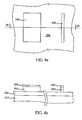
- FIG. 1 is a flow diagram illustrating a fabrication method embodiment of the invention.
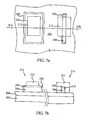
- FIGS. 2 a , 3 a , 4 a , 5 a , 6 a , and 7 a are top plan views of embodiments of capacitor structures of the invention during the fabrication method of FIG. 1.
- FIGS. 2 b , 3 b , 4 b , 5 b , 6 b , and 7 b are cross-sectional side views of embodiments of capacitor structures of the invention during the fabrication method of FIG. 1 taken along lines 2 b - 2 b , 3 b - 3 b , 4 b - 4 b , 5 b - 5 b , 6 b - 6 b , and 7 b - 7 b of FIGS. 2 a , 3 a , 4 a , 5 a , 6 a , and 7 a respectively.
- the present invention may be readily adapted to a variety of device designs and methods for forming the same that incorporate capacitors commonly used in planar complementary metal oxide semiconductor (CMOS) technology into a Fin field effect transistor (FinFET) based technology.
- CMOS complementary metal oxide semiconductor
- FinFET Fin field effect transistor
- the present invention provides at least one capacitor that includes at least one single-crystal Fin structure having a top surface and a first side surface opposite a second side surface. Adjacent the top surface of the at least one Fin structure is at least one insulator structure. Adjacent the at least one insulator structure and over a portion of the at least one Fin structure is at least one conductor structure.
- the decoupling capacitors of the invention and other circuit devices may be formed at the device level (i.e., the level in the integrated circuit (IC) at which transistors and other circuit elements are formed) using simple design changes within the same integration method, but without multiple different oxidations and depositions.
- the device level i.e., the level in the integrated circuit (IC) at which transistors and other circuit elements are formed
- different designs will yield any number, combination, and/or type of decoupling capacitors of the invention (e.g. nominal-voltage, high-voltage, implant variations of the foregoing, etc.), CMOS FinFET's, and/or other devices on the same substrate in order to provide effective decoupling capacitance in an area-efficient manner with superior high-frequency response.
- each step may correspond to a step which is already required in producing an IC.
- decoupling capacitors within the scope of the invention may be fabricated in steps entirely separate from those used in producing other devices on an IC, and using many alternate fabrication techniques.
- the invention is not limited to use of any specific dopant types provided that the dopant types selected for the various components are consistent with the intended electrical operation of the device.
- method 100 may form an IC with any number, combination, and/or type of decoupling capacitors of the present invention (e.g. nominal-voltage, high-voltage, implant variations of the foregoing, etc.), transistors (e.g. CMOS FinFETs), and/or other circuit devices by: providing an appropriate substrate, such as a SOI wafer for example; forming any number of narrow and/or broad Fins from SOI layer; forming and patterning insulator structures adjacent the Fins; forming and patterning conductor structures adjacent the insulator structures; and completing the IC.
- decoupling capacitors of the present invention e.g. nominal-voltage, high-voltage, implant variations of the foregoing, etc.
- transistors e.g. CMOS FinFETs
- other circuit devices by: providing an appropriate substrate, such as a SOI wafer for example; forming any number of narrow and/or broad Fins from SOI layer; forming and patterning insulator structures adjacent the Fins; forming and
- decoupling capacitors of the invention relate to fabrication. Each fabrication step employed to produce the various structures included in the decoupling capacitors may also be employed to produce portions of other devices elsewhere on the same substrate. Therefore, decoupling capacitors according to the invention may be produced as an adjunct to the production of the various devices included in the IC without requiring additional fabrication steps, thereby incurring essentially no additional process cost. This advantage of the decoupling capacitors applies to both the bulk semiconductor and SOI implementations to be discussed.
- first step 102 of method 100 is to provide an appropriate substrate.
- substrate 200 may comprise wafer 202 that underlies buried insulator 204 that underlies semiconductor layer 206 . Therefore, for example, substrate 200 may comprise a single-crystal SOI wafer.
- other substrate 200 embodiments may be used, such as a non-SOI wafer comprising only wafer 202 for example. When a non-SOI wafer embodiment is used, the processing remains otherwise identical to that of a SOI wafer embodiment, except as noted.
- Wafer 202 may be composed of any appropriate semiconducting material, including, but not limited to: Si, Ge, GaP, InAs, InP, SiGe, GaAs, or other III/V compounds.
- wafer 202 may comprise single-crystal silicon.
- Buried insulator 204 may be formed on wafer 202 using Separation by Implantation and Oxidation (SIMOX) or by wafer bonding and etch-back, or other techniques known in the art. Buried insulator 204 may comprise any insulative material, such as Buried Oxide (BOX). However, any type and/or combination of buried insulators may be used for buried insulator 204 .
- SIMOX Separation by Implantation and Oxidation
- BOX Buried Oxide
- any type and/or combination of buried insulators may be used for buried insulator 204 .
- Semiconductor layer 206 may be formed on buried insulator 204 by any technique known in the art, and may comprise any semiconductor material.
- semiconductor layer 206 comprises a single-crystal silicon-on-insulator (SOI) layer.
- SOI silicon-on-insulator
- Semiconductor layer 206 may have any height.
- semiconductor layer 206 may have a height between approximately 10 nm-160 nm. As will be made clear, the height semiconductor layer 206 may define the height of the Fins.
- step 104 of method 100 is to form narrow and/or broad Fins from semiconductor layer 206 , and therefore, any number, combination, and/or type of Fin-type decoupling capacitors of the invention, CMOS FinFETs, and/or other circuit devices.
- each Fin may act as a capacitive body (plate) in the case of a decoupling capacitor of the invention or as a transistor body in the case of a transistor; 2) each insulator structure formed adjacent the top surface, the first side surface, and/or the second opposing side surface of the respective Fin may act as capacitor dielectric in the case of a decoupling capacitor of the invention or as a gate dielectric in the case of a transistor; and 3) each conductor structure formed adjacent the insulator structure may act as an electrode (plate) in the case of a decoupling capacitor of the invention or as a gate in the case of a transistor.
- the narrow and/or broad Fins may be formed in any of the previously proposed techniques, such as Sidewall Image Transfer (SIT) technology and/or Conventional Image Transfer (CIT) technology. Accordingly, for the exemplary purposes of this disclosure, narrow and/or broad Fins may be formed from semiconductor layer 206 in step 104 through CIT in the following manner.
- SIT Sidewall Image Transfer
- CIT Conventional Image Transfer
- the first step is to deposit hard mask film 208 as depicted in FIGS. 2 a - 2 b .
- Hard mask film 208 acts as an etch stop layer and will be used throughout the Fin fabrication process when needed. Moreover, as will be made clear, a portion of hard mask film 208 forms what may be the capacitive dielectric for a high-voltage decoupling capacitor of the invention.
- hard mask film 208 may be silicon dioxide (SiO2) or silicon nitride (Si 3 N 4 ).
- a next step is implemented to pattern and etch hard mask film 208 by any technique known in the art.
- a suitable thin layer of photoresist (PR) may be used to cover the surface of hard mask film 208 .
- PR photoresist
- a mask or masks may be used to generate any pattern or patterns of narrow and/or broad lines on the PR overlying hard mask film 208 .
- This provides flexibility within substrate 200 to designate narrow and/or broad Fins, and therefore, any number, combination, and/or type of Fin-type decoupling capacitors of the invention, CMOS FinFETs, and/or other circuit devices.
- the particular narrow and/or broad Fin is defined by the appropriate mask to facilitate etching that Fin into substrate 200 .
- narrow and/or broad lines on the PR overlying hard mask film 208 are generated, then a suitable directional etch may be performed through hard mask film 208 to form narrow and/or broad lines in hard mask film 208 .
- narrow lines typically have a thickness in the range of approximately 0.3 nm to 40 nm, while broad lines typically have a thickness that is greater than 40 nm.
- the thickness of hard mask film 208 narrow and/or broad lines translates into the thickness of the narrow and/or broad Fins.
- the PR is then stripped away by a suitable chemical process, thereby resulting in hard mask film 208 narrow and/or broad lines on semiconductor layer 206 as depicted in FIGS. 3 a - 3 b.
- the next step is to anisotropically etch semiconductor layer 206 using hard mask film 208 narrow and/or broad lines, thereby forming narrow and/or broad Fins. This may be done using a suitable reactive ion etch (RIE) process that etches semiconductor layer 206 , stopping on buried insulator 204 .
- RIE reactive ion etch
- narrow and/or broad Fins may remain and may comprise portions of semiconductor layer 206 with respective hard mask film 208 narrow and/or broad lines adjacent their top surfaces.
- Each Fin may have a top surface that is substantially horizontal to buried insulator 204 and opposing vertical sidewalls or surfaces that are substantially perpendicular to buried insulator 204 .
- SIT may be used on substrate 200 so that only narrow Fins may be formed from semiconductor layer 206 , or SIT and CIT may be combined on substrate 200 so that both narrow and broad Fins may be formed from semiconductor layer 206 .
- SIT allows the respective gate or electrode length of the devices to have minimum feature size, while allowing the thickness of the Fin body to be much smaller than the respective gate or electrode length.
- the Fin body thickness is determined by the image of a sidewall spacer, allowing the Fin body to be reliably formed at sub minimum feature size.
- SIT involves the formation of at least one etch stop layer and a mandrel layer.
- the mandrel layer is then patterned, and sidewall spacers are formed adjacent the sidewalls of the patterned mandrel layer.
- the mandrel layer is selectively removed.
- the SOI layer is then etched selective to the sidewall spacers, and thus, narrow Fins are defined using SIT.
- hard mask film 208 (an etch stop layer) is formed on semiconductor layer 206 similar to that depicted in FIGS. 2 a - 2 b .
- Hard mask film 208 will be used throughout both the Fin fabrication process when needed.
- a mandrel layer is formed.
- the mandrel layer is a part of a sidewall image transfer which is used to define the narrow Fins.
- the mandrel layer is used to form sidewall spacers, which are in turn used to define the narrow hard mask film 208 lines.
- the mandrel layer may have a height of between 10 nm and 200 nm.
- the next steps are to pattern the mandrel layer, form sidewall spacers, remove the remaining mandrel layer, and pattern hard mask film 208 .
- a PR mask may be produced over the surface of the mandrel layer which defines the location of an edge of a narrow Fin to be produced later.
- a substantially vertical edge may be created through the mandrel layer.
- the PR mask may be removed.
- the sidewall spacers may then be formed adjacent the substantially vertical edge of the patterned mandrel layer. As will be shown later, the thickness of a sidewall spacer will define the thickness of the narrow Fin structure.
- the remaining mandrel layer is selectively removed.
- Etching of the mandrel layer may be done using a RIE process selective to the sidewall spacers and hard mask film 208 . Then a suitable directional etch is performed through hard mask film 208 stopping on semiconductor layer 206 , thereby forming hard mask film 208 narrow lines.
- the next step is to remove the sidewall spacers down to hard mask film 208 narrow lines.
- the sidewall spacers may be left in place.
- the final step is to pattern semiconductor layer 206 using the hard mask film 208 narrow lines as masks. This may be done using a suitable anisotropic etching process that etches semiconductor layer 206 stopping on buried insulator 204 . Additionally, it is generally desirable to have the thickness of the narrow Fins (i.e., the thickness of semiconductor layer 206 portions) less than the gate or electrode structure length. As the gate and electrode structure length is generally made to minimum feature size, SIT is used to achieve the subminimum feature size of the narrow Fins. Therefore, as described above, the thickness of the sidewall spacer determines the thickness of the narrow Fin.
- narrow Fins remain and comprise narrow portions of semiconductor layer 206 with overlying hard mask film 208 narrow lines similar to the narrow Fin that is depicted in FIGS. 4 a - 4 b.
- CIT may also be combined with SIT on substrate 200 so that both narrow and broad Fins may be formed from semiconductor layer 206 , since broad Fins may not be made with SIT. Accordingly, the CIT process described previously may simultaneously be implemented with the above SIT process so as to form broad Fins comprising broad portions of semiconductor layer 206 with overlying hard mask film 208 broad lines similar to the broad Fin that is depicted in FIGS. 4 a - 4 b . Particularly, for example, after the steps of forming sidewall spacers and removing the mandrel layer in the above SIT process, a suitable thin layer of PR may be used to cover another portion or portions of the surface of hard mask film 208 .
- a second alternative is to form the mandrels, then use a blocking mask to protect the CIT areas while SIT is carried out, then use a suitable etchant for the process.
- a mask or masks may be used to generate any pattern or patterns of narrow and/or broad lines on the PR overlying hard mask film 208 .
- two different masks for different portions of substrate 200 are used at the same patterning level (same lithography step), one being the mask for the SIT Narrow Fin(s) and the other being the mask for the CIT broad Fin(s).
- the FETs could be formed from either narrow or broad Fins; in practice, narrow Fins are preferred.
- a suitable directional etch may be performed through hard mask film 208 using the spacers and PR narrow and/or broad lines to form narrow and/or broad lines in hard mask film 208 .
- the spacers and PR narrow and/or broad lines are then stripped away by a suitable chemical process, thereby resulting in hard mask film 208 narrow and/or broad lines on semiconductor layer 206 similar to those depicted in FIGS. 3 a - 3 b.
- the next step is to anisotropically etch semiconductor layer 206 using hard mask film 208 .
- the final step is to pattern semiconductor layer 206 using the hard mask film 208 narrow and/or broad lines as masks, thereby forming narrow and/or broad Fins.
- narrow and/or broad Fins may remain similar to those depicted in FIGS. 4 a - 4 b.
- any or all of the Fins depicted in FIGS. 4 a - 4 b are formed by CIT and/or SIT, any or all of the Fins may then be lightly or heavily doped as needed so as to vary capacitive behavior in the case of decoupling capacitors of the invention or to form P-well structures and N-well structures in the case of NFETs and PFETs for example.
- this may include an ion implantation into the Fins in order to form and allow in substrate 200 the integration of nominal-voltage and high-voltage decoupling capacitors that are more ideal in their electrical behaviors.
- Phosphorus (P) is well suited for either type of decoupling capacitor.
- ion implantation may be done at a dose of 1-3 ⁇ 10 15 cm ⁇ 3 to dope a single-crystal silicon Fin to be 1 ⁇ 10 20 cm ⁇ 2 N-Type.
- Ion implantation may comprise an angled implant into exposed opposing vertical sidewalls of the Fins, and would serve to properly dope the Fins.
- doping may include an ion implantation into some of the Fins.
- P, As and Sb, for example, are well suited for PFETs.
- B, In and Ga, for example, are well suited for NFETs.
- Ion implantation is typically performed at a dose to achieve concentrations of between 1 ⁇ 10 17 cm ⁇ 3 to 5 ⁇ 10 18 cm ⁇ 3 for example.
- ion implantation may comprise an angled implant into exposed opposing vertical sidewalls of the Fins, and would serve to properly dope the Fins.
- a deposit/etch oxide process is used to deposit SiO 2 exclusively on the bottom horizontal surfaces of etched wafer 202 of a height approximately one-quarter the height of the etched Fins.
- the oxide may be doped, and some portion of the dopant out-diffused into those portions of the Fins immediately adjacent to the doped oxide. For example, in the case of FinFET's, this serves to suppress leakage in what will be non-gated sidewalls of the Fins, from source to drain.
- insulator layers 210 are formed on opposing vertical sidewalls of the narrow and/or broad Fins (i.e., semiconductor layer 206 portions) as depicted in FIGS. 5 a - 5 b .
- Insulator layers 210 may be formed by thermal oxidation, typically at 750-800 ⁇ ° C., or alternatively, may be formed by depositing a dielectric film.
- insulator layers 210 may be SiO 2 , a nitrided oxide material, a high-K dielectric material, or combinations thereof, as known in the art.
- insulator layers 210 on a narrow Fin form what may be the capacitive dielectric for a nominal-voltage decoupling capacitor of the invention.
- step 108 of method 100 is to form an overlying conductor layer 212 .
- Conductor layer 212 may be any suitable conducting material, typically a polycrystalline silicon material, although amorphous silicon, a combination of amorphous silicon and polysilicon, polysilicon-germanium, or any other appropriate material may be used to form gate conductor layer 212 .
- a metal conductor layer 212 such as W, Mo, or Ta, or any other refractory metal, or alternatively, a silicided metal conductor comprising polysilicon added with Ni or Co.
- conductor layer 212 encompass a silicon material
- such layers may be deposited as a doped layer (in-situ doping).
- conductor layer 212 is a metal layer
- such layers may be deposited using physical vapor or chemical vapor deposition methods or any other technique known in the art.
- step 110 of method 100 is to pattern conductor layer 212 .
- a hard mask film is formed and patterned to facilitate the patterning of conductor layer 212 .
- the hard mask film may be SiO 2 or Si 3 N 4 .
- step 110 next is to pattern conductor layer 212 .
- conductor layer 212 may be patterned and structured using well known photolithography and etching techniques (i.e., using the hard mask film as an etch block during a directional etching of conductor layer 212 ) to form, for example, electrodes for decoupling capacitors of the invention or gates for transistors.
- This may involve selectively removing portions of conductor layer 212 down to buried insulator 204 , but not removing the narrow and/or broad portions of semiconductor layer 206 forming the narrow and/or broad Fins that are protected by hard mask film 208 narrow and/or broad lines.
- nominal-voltage decoupling capacitor 214 and high-voltage decoupling capacitor 215 are depicted having a minimum of complexity. These depicted embodiments are at a stage of a process flow technique modified by an integration method of the present invention for forming any number, combination, and/or type of inventive decoupling capacitors, CMOS FinFET's, and/or other devices on the same substrate in order to provide effective decoupling capacitance in an area-efficient manner. Particularly, wafer 202 is depicted with an overlying buried insulator 204 .
- Nominal-voltage decoupling capacitor 214 comprises narrow semiconductor layer 206 portion (the narrow Fin) with overlying thick hard mask film 208 narrow line. Insulator layers 210 are formed on opposing vertical sidewalls of the narrow Fin. Conductor layer 212 portion is structured adjacent insulator layer 210 portions and hard mask film 208 narrow line portion, thereby encapsulating the narrow Fin.
- High-voltage decoupling capacitor 215 comprises broad semiconductor layer 206 portion (the broad Fin) with overlying thick hard mask film 208 narrow line. Insulator layers 210 are formed on opposing vertical sidewalls of the broad Fin.
- Conductor layer 212 portion is structured adjacent hard mask film 208 broad line portion so that conductor layer 212 portion is within a thickness of the broad Fin. It is advantageous for the conductor layer 212 portion to partially overlay (or be within the thickness) of the broad Fin. If conductor layer 212 portion extended beyond the thickness of the broad Fin, thereby becoming additionally adjacent to a sidewall of the broad Fin, then a region of thin insulator on the sidewall would be exposed to high electric fields when using this decoupling capacitor at higher voltages. This would result in significantly higher leakage currents through the capacitor and in decreased reliability.
- the decoupling capacitor embodiments of FIGS. 7 a - 7 b (and/or any other decoupling capacitor embodiments of the present invention), CMOS FinFETs, and/or other devices may be completed according to step 112 of method 100 . Accordingly, exposed portions of the Fins may be doped to form S/D regions (i.e. to produce FinFETs). The capacitor Fins may be masked during this step.
- the S/D regions may define, in semiconductor layer 206 portions comprising transistor bodies, channel regions underlying the gate stacks. Formation of the S/D regions may be accomplished using any of the variety of methods that have been developed to form S/D regions and that are tailored for specific performance requirements.
- lightly doped S/D regions or other S/D regions may be formed.
- lightly doped S/D regions or other S/D regions may be formed.
- NFETs typically P, As, or Sb for example is used for the S/D implants in the range of 1 to 5 keV and a dose of 5 ⁇ 10 14 to 2 ⁇ 10 15 cm ⁇ 2 .
- PFETs typically B, In, or Ga for example is used for the S/D implants in the range of 0.5 to 3 keV and dose of 5 ⁇ 10 14 to 2 ⁇ 10 15 cm ⁇ 2 .
- extension and halo implants may be formed that improve Short Channel Effects (SCE).
- SCE Short Channel Effects
- NFETs typically B, In, or Ga may be used for the halo implants with energies in the range of 5 to 15 keV and a dose of 1 ⁇ 1013 to 8 ⁇ 1013 cm ⁇ 2.
- P, As, or Sb may be used for the halos, with energies from 20 to 45 keV and dose of 1 ⁇ 1013 to 8 ⁇ 1013 cm ⁇ 2.
- interconnects, contacts, wiring layers (located above the device level), etc. may then be produced in metallization steps known in the art. Accordingly, sources, drains, and electrodes may be contacted by way of a local interconnect(s) where, for example, interconnects may be disposed adjacent conductor layer 212 portions, and/or interconnects may be disposed adjacent the top surfaces, the first side surfaces, and/or the opposing second side surfaces of the sources or drains (doped exposed portions of the Fins). Contacts to sources, drains, electrodes, and gates may also be formed, such that e.g. the top electrode 212 of a capacitor 215 and/or 214 would be coupled to the source electrode of a FinFET.
- a dielectric may be deposited and planarized typically using a chemical-mechanical polish process.
- Contact holes may then be structured and etched using an anisotropic process (e.g. reactive-ion etch) or the like.
- the contact holes may be filled using any conducting material, such as doped polysilicon, silicide (e.g. WSi), metals (e.g. Au, Al, Mo, W, Ta, Ti, Cu, or ITO (indium-tin oxide)), or the like, being deposited by evaporation, sputtering, or other known techniques, thereby forming contacts.
- the first metal layer may be deposited and structured using a RIE process or the like.
- the structuring of the first metal layer may be done following a damacene process flow.
- any number and combination of nominal-voltage decoupling capacitors, high-voltage decoupling capacitors, the implant variations of nominal-voltage and high-voltage decoupling capacitors, FinFETs, and/or other devices may be formed on substrate 200 .
- Fin-type decoupling capacitors may be used in many different kinds of circuits, such as high performance logic, low power logic or high density memory devices, including high density multi-gigabit DRAMs.
- inventive decoupling capacitors e.g. nominal-voltage and high-voltage
- the implant variations of each may readily be combined with each other and other elements, such as for example CMOS FinFETs, resistors, diodes, memory cells, and so forth, in any combination.
- inventive decoupling capacitors when the inventive decoupling capacitors are ion implanted to be more ideal in their electrical behaviors, they may be used in phase-lock loops where very ideal behavior is important, or other analog components.
- the high-voltage decoupling capacitor (whether ion implanted or not) may be used in a place where power supply voltage is considerably in excess of the on-chip core voltage. This often occurs in off-chip drivers or analog circuitry that may be on the same chip.
- the power supply for analog may be 2.5 V while the core logic may be at 1 V.
- the nominal-voltage decoupling capacitor (whether ion implanted or not) may be used as a decoupling capacitor for the main power supply for all the logic and to keep noise values low.
- the present invention may provide device designs and methods for incorporating capacitors commonly used in planar CMOS technology into a FinFET based technology.
- the decoupling capacitors of the invention and other circuit devices may be formed at the device level using simple design changes within the same integration method, but without multiple different oxidations and depositions.
- different designs will yield any number, combination, and/or type of decoupling capacitors of the invention (e.g. nominal-voltage, high-voltage, implant variations of the foregoing, etc.), CMOS FinFETs, and/or other devices on the same substrate in order to provide effective decoupling capacitance in an area-efficient manner with superior high-frequency response.
Abstract
Description
- The present invention relates generally to the field of semiconductor manufacturing and, more specifically, to Fin-type decoupling capacitors.
- In recent years, the need to remain cost and performance competitive in the production of semiconductor devices has caused continually increasing device density in integrated circuits. To facilitate the increase in device density, new technologies are constantly needed to allow the feature size of these semiconductor devices to be reduced.
- In the semiconductor industry, large, planar capacitors formed by two plates separated by a dielectric have been used in many semiconductor designs for the purpose of decoupling noise from power lines. In earlier integrated circuits, much of the decoupling capacitance could be placed off-chip due to the relatively slow cycle times at which such circuits operated. As semiconductor fabrication technologies advance, however, ever increasing device densities have resulted in a need to provide dense capacitors with high capacitance, for various purposes. For example, there are requirements for capacitors for certain analog circuits and functions. Another purpose may be for noise decoupling of power supply nodes. Additionally, the high switching rates used in a modern integrated circuit may cause the power supply voltage to degrade at certain points in the circuit and may cause circuit failures. Decoupling capacitors may be used to reduce supply voltage variations arising from high switching rates in the supplied circuits. These decoupling capacitors are connected between the supply voltage (V dd) and ground (Vss) in parallel with the supplied circuit. This parallel capacitance tends to decouple the voltage supply from disturbances induced by activity in the supplied circuit and allow the voltage supply to remain at the intended level.
- The slow frequency response of off-chip capacitance makes off-chip capacitor arrangements unsuitable for providing the decoupling capacitance necessary to prevent circuit failures in high speed integrated circuit devices.
- Accordingly, in order to provide sufficient decoupling capacitance for high frequency circuits, the capacitance must be moved closer to the switching circuitry, onto the integrated circuit chip itself. However, there are various areas of concern in on-chip decoupling capacitor design.
- First, the on-chip capacitance should be provided in an area-efficient manner so as not to take up excessive space on the respective chip. Furthermore, on-chip capacitors should be easy to fabricate along with the active and passive circuit elements which make up the desired integrated circuit (i.e., through the same integration). Moreover, different types of decoupling capacitors should be available on the same chip. For example, in certain applications it is desirable to have a thick oxide capacitor. A thick oxide capacitor has lower leakage and higher reliability, however it supplies less capacitance per unit area. Thus, tradeoffs must be made among leakage, reliability, and density. If leakage is less of a concern and the reliability tradeoffs are not big, then a thin oxide capacitor tends to be a better choice.
- Using a Fin field effect transistor (FinFET) based technology provides advantages toward high speed CMOS. FETs are the basic electrical devices of today's integrated circuits and are used in almost all types of integrated circuit design (i.e., microprocessors, memory, etc.). A FinFET is one type of FET that has been proposed to facilitate increased device performance. In a FinFET, a vertical “fin” shaped structure is defined to form the body of the transistor. Gates are then formed on one or both sides of the Fin. When gates are formed on both sides of the Fin, the transistor is generally referred to as a double gate FinFET. In particular, the use of the double gate suppresses Short Channel Effects (SCE), provides for lower leakage, and provides for more ideal switching behavior. In addition, the use of the double gate increases gate area, which allows the FinFET to have better current control, without increasing the gate length of the device. As such, the FinFET is able to have the current control of a larger transistor without requiring the device space of the larger transistor.
- However, using a FinFET based technology to solve the foregoing problems requires a redesign of capacitors. Thus, there is a need for improved and redesigned capacitor structures that incorporate capacitors commonly used in planar CMOS technology into a FinFET based technology.
- Accordingly, the invention provides device designs and methods for incorporating capacitors commonly used in planar complementary metal oxide semiconductor (CMOS) technology into a Fin field effect transistor (FinFET) based technology. The capacitors of the invention and other circuit devices may be formed at the device level (i.e., the level in the integrated circuit (IC) at which transistors and other circuit elements are formed) using simple design changes within the same integration method, but without multiple different oxidations and depositions. Thus, simultaneously in one integration method, different designs will yield any number, combination, and/or type of capacitors of the invention (e.g. nominal-voltage, high-voltage, implant variations of the foregoing, etc.), CMOS FinFETs, and/or other devices on the same substrate in order to provide effective decoupling capacitance in an area-efficient manner with superior high-frequency response.
- The capacitors of the invention may be implemented both in standard CMOS technology (commonly referred to as “bulk” semiconductor technology), and in silicon-on-insulator (SOI) technology. In addition, Sidewall Image Transfer (SIT) technology and/or Conventional Image Transfer (CIT) technology may be used to form the Fins for the various types of capacitors of the invention and other circuit devices.
- Generally, at least one capacitor of the invention includes at least one single-crystal Fin structure having a top surface and a first side surface opposite a second side surface. Adjacent the top surface of the Fin structure is at least one insulator structure. Adjacent the insulator structure and over a portion of the at least one Fin structure is at least one conductor structure.
- In one embodiment, the capacitor comprises a nominal-voltage decoupling capacitor. For this type of decoupling capacitor, the single-crystal Fin structure is narrow and the insulator structure is further adjacent both the first side surface and the second side surface of the Fin structure, thereby encapsulating the Fin structure. Thus, for example, a nominal-voltage decoupling capacitor according to the invention may be designed in the same manner as a FinFET except that the gate is used as one plate of the decoupling capacitor, the thin gate dielectric is used as the capacitive dielectric, and a source/drain (S/D) region formed from the Fin structure(typically connected in later processing steps) is used as the other plate. Additionally, after the narrow Fin structure is formed, it may be doped heavily or not to vary the capacitive behavior of the device.
- In another embodiment of the invention, the capacitor comprises a high-voltage decoupling capacitor. For this type of decoupling capacitor, the single-crystal Fin structure is broad and the conductor structure is within a thickness of the Fin structure. Thus, for example, a high-voltage decoupling capacitor according to the invention may be designed in the same manner as a FinFET except the remaining thick hardmask left after the broad Fin etch serves as the capacitive dielectric, the broad Fin serves as one plate, and the gate atop the thick dielectric and defined to be entirely within the thickness of the broad Fin serves as the other plate. Both plates may be contacted by way of a local interconnect. Additionally, as with the previous embodiment, after the broad Fin structure is formed, it may be doped heavily or not to vary the capacitive behavior of the device.
- In still another embodiment, the capacitor of the invention comprises a combination of nominal-voltage decoupling capacitors, high-voltage decoupling capacitors, and/or their implant variations.
- The foregoing and other features and advantages of the present invention will be apparent from the following more particular description of embodiments of the invention, as illustrated in the accompanying drawings.
- Embodiments of the present invention will hereinafter be described in conjunction with the appended drawings, where like designations denote like elements.
- FIG. 1 is a flow diagram illustrating a fabrication method embodiment of the invention.
- FIGS. 2 a, 3 a, 4 a, 5 a, 6 a, and 7 a are top plan views of embodiments of capacitor structures of the invention during the fabrication method of FIG. 1.
- FIGS. 2 b, 3 b, 4 b, 5 b, 6 b, and 7 b are cross-sectional side views of embodiments of capacitor structures of the invention during the fabrication method of FIG. 1 taken along
lines 2 b-2 b, 3 b-3 b, 4 b-4 b, 5 b-5 b, 6 b-6 b, and 7 b-7 b of FIGS. 2a, 3 a, 4 a, 5 a, 6 a, and 7 a respectively. - The present invention may be readily adapted to a variety of device designs and methods for forming the same that incorporate capacitors commonly used in planar complementary metal oxide semiconductor (CMOS) technology into a Fin field effect transistor (FinFET) based technology. Generally, the present invention provides at least one capacitor that includes at least one single-crystal Fin structure having a top surface and a first side surface opposite a second side surface. Adjacent the top surface of the at least one Fin structure is at least one insulator structure. Adjacent the at least one insulator structure and over a portion of the at least one Fin structure is at least one conductor structure.
- The decoupling capacitors of the invention and other circuit devices may be formed at the device level (i.e., the level in the integrated circuit (IC) at which transistors and other circuit elements are formed) using simple design changes within the same integration method, but without multiple different oxidations and depositions. Thus, simultaneously in one integration method, different designs will yield any number, combination, and/or type of decoupling capacitors of the invention (e.g. nominal-voltage, high-voltage, implant variations of the foregoing, etc.), CMOS FinFET's, and/or other devices on the same substrate in order to provide effective decoupling capacitance in an area-efficient manner with superior high-frequency response.
- It will be understood by one of ordinary skill in the art that the invention is not limited to the specific structures illustrated in the drawings, as the structures are shown in greatly exaggerated scale and boundary lines between materials in the structures may not form straight lines as depicted for purposes of illustration in the drawings. It will also be understood by one of ordinary skill in the art that the invention is not limited to the specific fabrication steps detailed herein. Numerous semiconductor fabrication processes may be used to produce a decoupling capacitor embodying the principles of the invention. As will be made clear, the decoupling capacitors of the invention and other semiconductor devices may be implemented both in standard CMOS technology (commonly referred to as “bulk” semiconductor technology), and in silicon-on-insulator (SOI) technology. These processes are advantageous because each step may correspond to a step which is already required in producing an IC. However, decoupling capacitors within the scope of the invention may be fabricated in steps entirely separate from those used in producing other devices on an IC, and using many alternate fabrication techniques. Moreover, it will also be understood by one of ordinary skill in the art that the invention is not limited to use of any specific dopant types provided that the dopant types selected for the various components are consistent with the intended electrical operation of the device.
- Turning now to FIG. 1,
exemplary integration method 100 for forming an IC in accordance with the present invention is illustrated. Generally, and for the exemplary purposes of this disclosure,method 100 may form an IC with any number, combination, and/or type of decoupling capacitors of the present invention (e.g. nominal-voltage, high-voltage, implant variations of the foregoing, etc.), transistors (e.g. CMOS FinFETs), and/or other circuit devices by: providing an appropriate substrate, such as a SOI wafer for example; forming any number of narrow and/or broad Fins from SOI layer; forming and patterning insulator structures adjacent the Fins; forming and patterning conductor structures adjacent the insulator structures; and completing the IC. - As will be made clear, an important advantage of the decoupling capacitors of the invention relates to fabrication. Each fabrication step employed to produce the various structures included in the decoupling capacitors may also be employed to produce portions of other devices elsewhere on the same substrate. Therefore, decoupling capacitors according to the invention may be produced as an adjunct to the production of the various devices included in the IC without requiring additional fabrication steps, thereby incurring essentially no additional process cost. This advantage of the decoupling capacitors applies to both the bulk semiconductor and SOI implementations to be discussed.
- Accordingly,
first step 102 ofmethod 100 is to provide an appropriate substrate. Referring to the substrate embodiment depicted in FIGS. 2a-2 b,substrate 200 may comprisewafer 202 that underlies buriedinsulator 204 that underliessemiconductor layer 206. Therefore, for example,substrate 200 may comprise a single-crystal SOI wafer. However,other substrate 200 embodiments may be used, such as a non-SOI wafer comprisingonly wafer 202 for example. When a non-SOI wafer embodiment is used, the processing remains otherwise identical to that of a SOI wafer embodiment, except as noted. - Still referring to FIGS. 2 a-2 b, while
wafer 202 is depicted as having a minimum of complexity, other wafers of varying complexity may be advantageously employed.Wafer 202 may be composed of any appropriate semiconducting material, including, but not limited to: Si, Ge, GaP, InAs, InP, SiGe, GaAs, or other III/V compounds. For the exemplary purposes of this disclosure,wafer 202 may comprise single-crystal silicon. - Buried
insulator 204 may be formed onwafer 202 using Separation by Implantation and Oxidation (SIMOX) or by wafer bonding and etch-back, or other techniques known in the art.Buried insulator 204 may comprise any insulative material, such as Buried Oxide (BOX). However, any type and/or combination of buried insulators may be used for buriedinsulator 204. -
Semiconductor layer 206 may be formed on buriedinsulator 204 by any technique known in the art, and may comprise any semiconductor material. For the exemplary purposes of this disclosure,semiconductor layer 206 comprises a single-crystal silicon-on-insulator (SOI) layer.Semiconductor layer 206 may have any height. For the exemplary purposes of this disclosure,semiconductor layer 206 may have a height between approximately 10 nm-160 nm. As will be made clear, theheight semiconductor layer 206 may define the height of the Fins. - Turning now to FIGS. 2 a-4 b, step 104 of
method 100 is to form narrow and/or broad Fins fromsemiconductor layer 206, and therefore, any number, combination, and/or type of Fin-type decoupling capacitors of the invention, CMOS FinFETs, and/or other circuit devices. For example, as will be made clear: 1) a portion of each Fin may act as a capacitive body (plate) in the case of a decoupling capacitor of the invention or as a transistor body in the case of a transistor; 2) each insulator structure formed adjacent the top surface, the first side surface, and/or the second opposing side surface of the respective Fin may act as capacitor dielectric in the case of a decoupling capacitor of the invention or as a gate dielectric in the case of a transistor; and 3) each conductor structure formed adjacent the insulator structure may act as an electrode (plate) in the case of a decoupling capacitor of the invention or as a gate in the case of a transistor. - The narrow and/or broad Fins may be formed in any of the previously proposed techniques, such as Sidewall Image Transfer (SIT) technology and/or Conventional Image Transfer (CIT) technology. Accordingly, for the exemplary purposes of this disclosure, narrow and/or broad Fins may be formed from
semiconductor layer 206 instep 104 through CIT in the following manner. - The first step is to deposit
hard mask film 208 as depicted in FIGS. 2a-2 b.Hard mask film 208 acts as an etch stop layer and will be used throughout the Fin fabrication process when needed. Moreover, as will be made clear, a portion ofhard mask film 208 forms what may be the capacitive dielectric for a high-voltage decoupling capacitor of the invention. For the exemplary purposes of this disclosure,hard mask film 208 may be silicon dioxide (SiO2) or silicon nitride (Si3N4). - A next step is implemented to pattern and etch
hard mask film 208 by any technique known in the art. For example, a suitable thin layer of photoresist (PR) may be used to cover the surface ofhard mask film 208. Next, a mask or masks may be used to generate any pattern or patterns of narrow and/or broad lines on the PR overlyinghard mask film 208. This provides flexibility withinsubstrate 200 to designate narrow and/or broad Fins, and therefore, any number, combination, and/or type of Fin-type decoupling capacitors of the invention, CMOS FinFETs, and/or other circuit devices. As will be made clear, the particular narrow and/or broad Fin is defined by the appropriate mask to facilitate etching that Fin intosubstrate 200. - Once the narrow and/or broad lines on the PR overlying
hard mask film 208 are generated, then a suitable directional etch may be performed throughhard mask film 208 to form narrow and/or broad lines inhard mask film 208. For example, narrow lines typically have a thickness in the range of approximately 0.3 nm to 40 nm, while broad lines typically have a thickness that is greater than 40 nm. As will be made clear, the thickness ofhard mask film 208 narrow and/or broad lines translates into the thickness of the narrow and/or broad Fins. The PR is then stripped away by a suitable chemical process, thereby resulting inhard mask film 208 narrow and/or broad lines onsemiconductor layer 206 as depicted in FIGS. 3a-3 b. - The next step is to anisotropically etch
semiconductor layer 206 usinghard mask film 208 narrow and/or broad lines, thereby forming narrow and/or broad Fins. This may be done using a suitable reactive ion etch (RIE) process that etchessemiconductor layer 206, stopping on buriedinsulator 204. - Thus, as depicted in FIGS. 4 a-4 b, narrow and/or broad Fins may remain and may comprise portions of
semiconductor layer 206 with respectivehard mask film 208 narrow and/or broad lines adjacent their top surfaces. Each Fin may have a top surface that is substantially horizontal to buriedinsulator 204 and opposing vertical sidewalls or surfaces that are substantially perpendicular to buriedinsulator 204. - Alternatively, for the exemplary purposes of this disclosure, in
step 104, SIT may be used onsubstrate 200 so that only narrow Fins may be formed fromsemiconductor layer 206, or SIT and CIT may be combined onsubstrate 200 so that both narrow and broad Fins may be formed fromsemiconductor layer 206. SIT allows the respective gate or electrode length of the devices to have minimum feature size, while allowing the thickness of the Fin body to be much smaller than the respective gate or electrode length. The Fin body thickness is determined by the image of a sidewall spacer, allowing the Fin body to be reliably formed at sub minimum feature size. - Generally, SIT involves the formation of at least one etch stop layer and a mandrel layer. The mandrel layer is then patterned, and sidewall spacers are formed adjacent the sidewalls of the patterned mandrel layer. Next, the mandrel layer is selectively removed. The SOI layer is then etched selective to the sidewall spacers, and thus, narrow Fins are defined using SIT.
- More particularly, and for the exemplary purposes of this disclosure, in the first step of forming the narrow Fins from
semiconductor layer 206, hard mask film 208 (an etch stop layer) is formed onsemiconductor layer 206 similar to that depicted in FIGS. 2a-2 b.Hard mask film 208 will be used throughout both the Fin fabrication process when needed. - Next, a mandrel layer is formed. As will be explained in greater detail later, the mandrel layer is a part of a sidewall image transfer which is used to define the narrow Fins. As such, the mandrel layer is used to form sidewall spacers, which are in turn used to define the narrow
hard mask film 208 lines. The mandrel layer may have a height of between 10 nm and 200 nm. - The next steps are to pattern the mandrel layer, form sidewall spacers, remove the remaining mandrel layer, and pattern
hard mask film 208. In patterning the mandrel layer, a PR mask may be produced over the surface of the mandrel layer which defines the location of an edge of a narrow Fin to be produced later. Then, by anisotropic etching, a substantially vertical edge may be created through the mandrel layer. Afterward, the PR mask may be removed. The sidewall spacers may then be formed adjacent the substantially vertical edge of the patterned mandrel layer. As will be shown later, the thickness of a sidewall spacer will define the thickness of the narrow Fin structure. The remaining mandrel layer is selectively removed. Etching of the mandrel layer may be done using a RIE process selective to the sidewall spacers andhard mask film 208. Then a suitable directional etch is performed throughhard mask film 208 stopping onsemiconductor layer 206, thereby forminghard mask film 208 narrow lines. - The next step is to remove the sidewall spacers down to
hard mask film 208 narrow lines. Optionally, the sidewall spacers may be left in place. - The final step is to
pattern semiconductor layer 206 using thehard mask film 208 narrow lines as masks. This may be done using a suitable anisotropic etching process that etchessemiconductor layer 206 stopping on buriedinsulator 204. Additionally, it is generally desirable to have the thickness of the narrow Fins (i.e., the thickness ofsemiconductor layer 206 portions) less than the gate or electrode structure length. As the gate and electrode structure length is generally made to minimum feature size, SIT is used to achieve the subminimum feature size of the narrow Fins. Therefore, as described above, the thickness of the sidewall spacer determines the thickness of the narrow Fin. - Thus, narrow Fins remain and comprise narrow portions of
semiconductor layer 206 with overlyinghard mask film 208 narrow lines similar to the narrow Fin that is depicted in FIGS. 4a-4 b. - Notwithstanding, CIT may also be combined with SIT on
substrate 200 so that both narrow and broad Fins may be formed fromsemiconductor layer 206, since broad Fins may not be made with SIT. Accordingly, the CIT process described previously may simultaneously be implemented with the above SIT process so as to form broad Fins comprising broad portions ofsemiconductor layer 206 with overlyinghard mask film 208 broad lines similar to the broad Fin that is depicted in FIGS. 4a-4 b. Particularly, for example, after the steps of forming sidewall spacers and removing the mandrel layer in the above SIT process, a suitable thin layer of PR may be used to cover another portion or portions of the surface ofhard mask film 208. Another alternative can be is to simply use a blocking mask over areas where broad Fins will be formed while carrying out the SIT process, then use a blocking mask that protects the sidewall spacers while the CIT process is carried out. Alternatively, these processes could be reversed. A second alternative is to form the mandrels, then use a blocking mask to protect the CIT areas while SIT is carried out, then use a suitable etchant for the process. Next, a mask or masks may be used to generate any pattern or patterns of narrow and/or broad lines on the PR overlyinghard mask film 208. Thus, in effect, two different masks for different portions ofsubstrate 200 are used at the same patterning level (same lithography step), one being the mask for the SIT Narrow Fin(s) and the other being the mask for the CIT broad Fin(s). Note that the FETs could be formed from either narrow or broad Fins; in practice, narrow Fins are preferred. - Then, a suitable directional etch may be performed through
hard mask film 208 using the spacers and PR narrow and/or broad lines to form narrow and/or broad lines inhard mask film 208. The spacers and PR narrow and/or broad lines are then stripped away by a suitable chemical process, thereby resulting inhard mask film 208 narrow and/or broad lines onsemiconductor layer 206 similar to those depicted in FIGS. 3a-3 b. - The next step is to anisotropically etch
semiconductor layer 206 usinghard mask film 208. The final step is topattern semiconductor layer 206 using thehard mask film 208 narrow and/or broad lines as masks, thereby forming narrow and/or broad Fins. Thus, narrow and/or broad Fins may remain similar to those depicted in FIGS. 4a-4 b. - Whether the narrow and/or broad Fins depicted in FIGS. 4 a-4 b are formed by CIT and/or SIT, any or all of the Fins may then be lightly or heavily doped as needed so as to vary capacitive behavior in the case of decoupling capacitors of the invention or to form P-well structures and N-well structures in the case of NFETs and PFETs for example. In the case of decoupling capacitors of the invention, this may include an ion implantation into the Fins in order to form and allow in
substrate 200 the integration of nominal-voltage and high-voltage decoupling capacitors that are more ideal in their electrical behaviors. Phosphorus (P), for example, is well suited for either type of decoupling capacitor. For example, ion implantation may be done at a dose of 1-3×1015 cm−3 to dope a single-crystal silicon Fin to be 1×1020 cm−2 N-Type. Ion implantation may comprise an angled implant into exposed opposing vertical sidewalls of the Fins, and would serve to properly dope the Fins. - In the case of NFETs and PFETs, doping may include an ion implantation into some of the Fins. P, As and Sb, for example, are well suited for PFETs. B, In and Ga, for example, are well suited for NFETs. Ion implantation is typically performed at a dose to achieve concentrations of between 1×10 17 cm−3 to 5×1018 cm−3 for example. Again, ion implantation may comprise an angled implant into exposed opposing vertical sidewalls of the Fins, and would serve to properly dope the Fins.
- When a non-SOI wafer embodiment is used, such as just
wafer 202 for example, after the Fins are etched by time to the desired depth (typically approximately 100 nm-200 nm belowwafer 202 surface), a deposit/etch oxide process is used to deposit SiO2 exclusively on the bottom horizontal surfaces of etchedwafer 202 of a height approximately one-quarter the height of the etched Fins. The oxide may be doped, and some portion of the dopant out-diffused into those portions of the Fins immediately adjacent to the doped oxide. For example, in the case of FinFET's, this serves to suppress leakage in what will be non-gated sidewalls of the Fins, from source to drain. - Turning to step 106 of
method 100, insulator layers 210 are formed on opposing vertical sidewalls of the narrow and/or broad Fins (i.e.,semiconductor layer 206 portions) as depicted in FIGS. 5a-5 b. Insulator layers 210 may be formed by thermal oxidation, typically at 750-800 ° C., or alternatively, may be formed by depositing a dielectric film. For the exemplary purposes of this disclosure, insulator layers 210 may be SiO2, a nitrided oxide material, a high-K dielectric material, or combinations thereof, as known in the art. As will be made clear, insulator layers 210 on a narrow Fin form what may be the capacitive dielectric for a nominal-voltage decoupling capacitor of the invention. - As depicted in FIGS. 6 a-6 b, step 108 of
method 100 is to form anoverlying conductor layer 212.Conductor layer 212 may be any suitable conducting material, typically a polycrystalline silicon material, although amorphous silicon, a combination of amorphous silicon and polysilicon, polysilicon-germanium, or any other appropriate material may be used to formgate conductor layer 212. In addition, in some embodiments of the present invention, it might be advantageous to employ ametal conductor layer 212, such as W, Mo, or Ta, or any other refractory metal, or alternatively, a silicided metal conductor comprising polysilicon added with Ni or Co. Instep 108, whereconductor layer 212 encompass a silicon material, such layers may be deposited as a doped layer (in-situ doping). Whereconductor layer 212 is a metal layer, such layers may be deposited using physical vapor or chemical vapor deposition methods or any other technique known in the art. - Turning to FIGS. 7 a-7 b, the
next step 110 ofmethod 100 is topattern conductor layer 212. To implementstep 110, a hard mask film is formed and patterned to facilitate the patterning ofconductor layer 212. Typically, the hard mask film may be SiO2 or Si3N4. Continuing withstep 110, next is topattern conductor layer 212. Accordingly,conductor layer 212 may be patterned and structured using well known photolithography and etching techniques (i.e., using the hard mask film as an etch block during a directional etching of conductor layer 212) to form, for example, electrodes for decoupling capacitors of the invention or gates for transistors. This may involve selectively removing portions ofconductor layer 212 down to buriedinsulator 204, but not removing the narrow and/or broad portions ofsemiconductor layer 206 forming the narrow and/or broad Fins that are protected byhard mask film 208 narrow and/or broad lines. - Thus, for example, in FIGS. 7 a-7 b, nominal-
voltage decoupling capacitor 214 and high-voltage decoupling capacitor 215 are depicted having a minimum of complexity. These depicted embodiments are at a stage of a process flow technique modified by an integration method of the present invention for forming any number, combination, and/or type of inventive decoupling capacitors, CMOS FinFET's, and/or other devices on the same substrate in order to provide effective decoupling capacitance in an area-efficient manner. Particularly,wafer 202 is depicted with an overlying buriedinsulator 204. On top of buriedinsulator 204 are nominal-voltage decoupling capacitor 214 and high-voltage decoupling capacitor 215. Nominal-voltage decoupling capacitor 214 comprisesnarrow semiconductor layer 206 portion (the narrow Fin) with overlying thickhard mask film 208 narrow line. Insulator layers 210 are formed on opposing vertical sidewalls of the narrow Fin.Conductor layer 212 portion is structuredadjacent insulator layer 210 portions andhard mask film 208 narrow line portion, thereby encapsulating the narrow Fin. High-voltage decoupling capacitor 215 comprisesbroad semiconductor layer 206 portion (the broad Fin) with overlying thickhard mask film 208 narrow line. Insulator layers 210 are formed on opposing vertical sidewalls of the broad Fin.Conductor layer 212 portion is structured adjacenthard mask film 208 broad line portion so thatconductor layer 212 portion is within a thickness of the broad Fin. It is advantageous for theconductor layer 212 portion to partially overlay (or be within the thickness) of the broad Fin. Ifconductor layer 212 portion extended beyond the thickness of the broad Fin, thereby becoming additionally adjacent to a sidewall of the broad Fin, then a region of thin insulator on the sidewall would be exposed to high electric fields when using this decoupling capacitor at higher voltages. This would result in significantly higher leakage currents through the capacitor and in decreased reliability. - The decoupling capacitor embodiments of FIGS. 7 a-7 b (and/or any other decoupling capacitor embodiments of the present invention), CMOS FinFETs, and/or other devices may be completed according to step 112 of
method 100. Accordingly, exposed portions of the Fins may be doped to form S/D regions (i.e. to produce FinFETs). The capacitor Fins may be masked during this step. For example, the S/D regions may define, insemiconductor layer 206 portions comprising transistor bodies, channel regions underlying the gate stacks. Formation of the S/D regions may be accomplished using any of the variety of methods that have been developed to form S/D regions and that are tailored for specific performance requirements. There are many such methods for forming S/D regions having various levels of complexity. Thus, in some embodiments of the present invention, using ion implantation for example, lightly doped S/D regions or other S/D regions may be formed. Thus, for example, for NFETs, typically P, As, or Sb for example is used for the S/D implants in the range of 1 to 5 keV and a dose of 5×10¹⁴ to 2×1015 cm−2. Similarly, for PFETs, typically B, In, or Ga for example is used for the S/D implants in the range of 0.5 to 3 keV and dose of 5×10¹⁴ to 2×1015 cm−2. - Optionally, extension and halo implants may be formed that improve Short Channel Effects (SCE). For NFETs, typically B, In, or Ga may be used for the halo implants with energies in the range of 5 to 15 keV and a dose of 1×10¹³ to 8×1013 cm−2. Similarly, for PFETs, P, As, or Sb may be used for the halos, with energies from 20 to 45 keV and dose of 1×10¹³ to 8×1013 cm−2.
- Continuing with
step 112, interconnects, contacts, wiring layers (located above the device level), etc. may then be produced in metallization steps known in the art. Accordingly, sources, drains, and electrodes may be contacted by way of a local interconnect(s) where, for example, interconnects may be disposedadjacent conductor layer 212 portions, and/or interconnects may be disposed adjacent the top surfaces, the first side surfaces, and/or the opposing second side surfaces of the sources or drains (doped exposed portions of the Fins). Contacts to sources, drains, electrodes, and gates may also be formed, such that e.g. thetop electrode 212 of acapacitor 215 and/or 214 would be coupled to the source electrode of a FinFET. For example, a dielectric may be deposited and planarized typically using a chemical-mechanical polish process. Contact holes may then be structured and etched using an anisotropic process (e.g. reactive-ion etch) or the like. The contact holes may be filled using any conducting material, such as doped polysilicon, silicide (e.g. WSi), metals (e.g. Au, Al, Mo, W, Ta, Ti, Cu, or ITO (indium-tin oxide)), or the like, being deposited by evaporation, sputtering, or other known techniques, thereby forming contacts. Then the first metal layer may be deposited and structured using a RIE process or the like. Alternatively, the structuring of the first metal layer may be done following a damacene process flow. - Thus, simultaneously with one integration method, any number and combination of nominal-voltage decoupling capacitors, high-voltage decoupling capacitors, the implant variations of nominal-voltage and high-voltage decoupling capacitors, FinFETs, and/or other devices may be formed on
substrate 200. - Fin-type decoupling capacitors according to the present invention may be used in many different kinds of circuits, such as high performance logic, low power logic or high density memory devices, including high density multi-gigabit DRAMs. Moreover, as previously illustrated and described, the inventive decoupling capacitors (e.g. nominal-voltage and high-voltage), along with the implant variations of each, may readily be combined with each other and other elements, such as for example CMOS FinFETs, resistors, diodes, memory cells, and so forth, in any combination.
- Describing uses of the inventive decoupling capacitors further by way of particular examples, when the inventive decoupling capacitors are ion implanted to be more ideal in their electrical behaviors, they may be used in phase-lock loops where very ideal behavior is important, or other analog components. The high-voltage decoupling capacitor (whether ion implanted or not) may be used in a place where power supply voltage is considerably in excess of the on-chip core voltage. This often occurs in off-chip drivers or analog circuitry that may be on the same chip. The power supply for analog may be 2.5 V while the core logic may be at 1 V. The nominal-voltage decoupling capacitor (whether ion implanted or not) may be used as a decoupling capacitor for the main power supply for all the logic and to keep noise values low.
- In summary, the present invention may provide device designs and methods for incorporating capacitors commonly used in planar CMOS technology into a FinFET based technology. The decoupling capacitors of the invention and other circuit devices may be formed at the device level using simple design changes within the same integration method, but without multiple different oxidations and depositions. Thus, simultaneously in one integration method, different designs will yield any number, combination, and/or type of decoupling capacitors of the invention (e.g. nominal-voltage, high-voltage, implant variations of the foregoing, etc.), CMOS FinFETs, and/or other devices on the same substrate in order to provide effective decoupling capacitance in an area-efficient manner with superior high-frequency response.
- The embodiments and examples set forth herein were presented in order to best explain the present invention and its practical application and to thereby enable those of ordinary skill in the art to make and use the invention. However, those of ordinary skill in the art will recognize that the foregoing description and examples have been presented for the purposes of illustration and example only. For example, the description as set forth is not intended to be exhaustive or to limit the invention to the precise form disclosed. Many modifications and variations are possible in light of the teachings above without departing from the spirit and scope of the forthcoming claims. Accordingly, unless otherwise specified, any components of the present invention indicated in the drawings or herein are given as an example of possible components and not as a limitation. Similarly, unless otherwise specified, any steps or sequence of steps of the method of the present invention indicated herein are given as examples of possible steps or sequence of steps and not as limitations.
Claims (19)
Priority Applications (2)
| Application Number | Priority Date | Filing Date | Title |
|---|---|---|---|
| US10/063,331 US6995412B2 (en) | 2002-04-12 | 2002-04-12 | Integrated circuit with capacitors having a fin structure |
| US11/216,862 US7060553B2 (en) | 2002-04-12 | 2005-08-31 | Formation of capacitor having a Fin structure |
Applications Claiming Priority (1)
| Application Number | Priority Date | Filing Date | Title |
|---|---|---|---|
| US10/063,331 US6995412B2 (en) | 2002-04-12 | 2002-04-12 | Integrated circuit with capacitors having a fin structure |
Related Child Applications (1)
| Application Number | Title | Priority Date | Filing Date |
|---|---|---|---|
| US11/216,862 Division US7060553B2 (en) | 2002-04-12 | 2005-08-31 | Formation of capacitor having a Fin structure |
Publications (2)
| Publication Number | Publication Date |
|---|---|
| US20030193058A1 true US20030193058A1 (en) | 2003-10-16 |
| US6995412B2 US6995412B2 (en) | 2006-02-07 |
Family
ID=28789684
Family Applications (2)
| Application Number | Title | Priority Date | Filing Date |
|---|---|---|---|
| US10/063,331 Expired - Fee Related US6995412B2 (en) | 2002-04-12 | 2002-04-12 | Integrated circuit with capacitors having a fin structure |
| US11/216,862 Expired - Lifetime US7060553B2 (en) | 2002-04-12 | 2005-08-31 | Formation of capacitor having a Fin structure |
Family Applications After (1)
| Application Number | Title | Priority Date | Filing Date |
|---|---|---|---|
| US11/216,862 Expired - Lifetime US7060553B2 (en) | 2002-04-12 | 2005-08-31 | Formation of capacitor having a Fin structure |
Country Status (1)
| Country | Link |
|---|---|
| US (2) | US6995412B2 (en) |
Cited By (40)
| Publication number | Priority date | Publication date | Assignee | Title |
|---|---|---|---|---|
| US20040262698A1 (en) * | 2003-06-25 | 2004-12-30 | International Business Machines Corporation | High-density finfet integration scheme |
| US20050161739A1 (en) * | 2004-01-28 | 2005-07-28 | International Business Machines Corporation | Method and structure to create multiple device widths in finfet technology in both bulk and soi |
| US6947275B1 (en) | 2004-10-18 | 2005-09-20 | International Business Machines Corporation | Fin capacitor |
| US6949768B1 (en) | 2004-10-18 | 2005-09-27 | International Business Machines Corporation | Planar substrate devices integrated with finfets and method of manufacture |
| US20060008927A1 (en) * | 2004-06-29 | 2006-01-12 | International Business Machines Corporation | Dual gated finfet gain cell |
| US20060073394A1 (en) * | 2004-10-04 | 2006-04-06 | International Business Machines Corporation | Reduced mask count gate conductor definition |
| US20060081895A1 (en) * | 2004-10-19 | 2006-04-20 | Deok-Huyng Lee | Semiconductor device having fin transistor and planar transistor and associated methods of manufacture |
| US20060145259A1 (en) * | 2004-12-30 | 2006-07-06 | Park Jeong H | Fin field-effect transistor and method for fabricating the same |
| US20060151834A1 (en) * | 2005-01-13 | 2006-07-13 | International Business Machines Corporation | High mobility plane finfet with equal drive strength |
| KR100620065B1 (en) | 2005-09-08 | 2006-09-06 | 주식회사 하이닉스반도체 | Semiconductor device and method for fabrication of the same |
| US20070010049A1 (en) * | 2005-06-21 | 2007-01-11 | International Business Machines Corporation | Thermal dissipation structures for finfets |
| US20070018201A1 (en) * | 2005-07-22 | 2007-01-25 | Michael Specht | Non-volatile memory cells and methods for fabricating non-volatile memory cells |
| US20070018239A1 (en) * | 2005-07-20 | 2007-01-25 | International Business Machines Corporation | Sea-of-fins structure on a semiconductor substrate and method of fabrication |
| US20070059891A1 (en) * | 2005-09-14 | 2007-03-15 | International Business Machines Corporation | Mandrel/trim alignment in SIT processing |
| US20080157269A1 (en) * | 2007-01-03 | 2008-07-03 | International Business Machines Corporation | Reversible electric fuse and antifuse structures for semiconductor devices |
| US20080157201A1 (en) * | 2006-12-28 | 2008-07-03 | Texas Instruments Incorporated | Electrically Programmable Fuse |
| US20080206934A1 (en) * | 2007-02-23 | 2008-08-28 | Jones Robert E | Forming semiconductor fins using a sacrificial fin |
| US20080224217A1 (en) * | 2007-03-13 | 2008-09-18 | Infineon Technologies | Mugfet switch |
| US20080274600A1 (en) * | 2007-05-04 | 2008-11-06 | Freescale Semiconductor, Inc. | Method to improve source/drain parasitics in vertical devices |
| US20110175152A1 (en) * | 2010-01-19 | 2011-07-21 | International Business Machines Corporation | Method and structure for forming high performance mos capacitor along with fully depleted semiconductor on insulator devices on the same chip |
| WO2011149587A1 (en) * | 2010-05-27 | 2011-12-01 | International Business Machines Corporation | Integrated circuit with finfets and mim fin capacitor |
| US20120146145A1 (en) * | 2010-10-21 | 2012-06-14 | International Business Machines Corporation | Semiconductor structure and methods of manufacture |
| US8581320B1 (en) * | 2012-05-15 | 2013-11-12 | International Business Machines Corporation | MOS capacitors with a finfet process |
| KR101385718B1 (en) * | 2011-12-29 | 2014-04-17 | 타이완 세미콘덕터 매뉴팩쳐링 컴퍼니 리미티드 | Mandrel modification for achieving single fin fin-like field effect transistor (finfet) device |
| US8716156B1 (en) | 2013-02-01 | 2014-05-06 | Globalfoundries Inc. | Methods of forming fins for a FinFET semiconductor device using a mandrel oxidation process |
| US20140124863A1 (en) * | 2012-11-07 | 2014-05-08 | International Business Machines Corporation | Method and structure for forming a localized soi finfet |
| US20140183610A1 (en) * | 2012-12-28 | 2014-07-03 | Taiwan Semiconductor Manufacturing Company, Ltd. | Decoupling Capacitor for FinFET Compatible Process |
| US20140209854A1 (en) * | 2013-01-28 | 2014-07-31 | International Business Machines Corporation | Nanowire Capacitor for Bidirectional Operation |
| US8859355B1 (en) * | 2013-05-06 | 2014-10-14 | International Business Machines Corporation | Method to make dual material finFET on same substrate |
| TWI483386B (en) * | 2007-03-27 | 2015-05-01 | Intel Corp | On-chip memory cell and method of manufacturing same |
| US9105506B2 (en) | 2011-06-21 | 2015-08-11 | Etron Technology, Inc. | Dynamic memory structure |
| US20150294913A1 (en) * | 2013-05-06 | 2015-10-15 | International Business Machines Corporation | Method to make dual material finfet on same substrate |
| US9373678B2 (en) | 2014-06-17 | 2016-06-21 | Globalfoundries Inc. | Non-planar capacitors with finely tuned capacitance values and methods of forming the non-planar capacitors |
| US20160211262A1 (en) * | 2013-09-25 | 2016-07-21 | Walid M. Hafez | Isolation well doping with solid-state diffusion sources for finfet architectures |
| US9455250B1 (en) * | 2015-06-30 | 2016-09-27 | International Business Machines Corporation | Distributed decoupling capacitor |
| CN106252417A (en) * | 2012-03-19 | 2016-12-21 | 三星电子株式会社 | There is the semiconductor device that different fin is wide |
| US9536939B1 (en) | 2015-10-28 | 2017-01-03 | International Business Machines Corporation | High density vertically integrated FEOL MIM capacitor |
| US9793263B1 (en) * | 2016-05-25 | 2017-10-17 | International Business Machines Corporation | Digital alloy FinFET co-integrated with passive resistor with good temperature coefficient |
| US10727224B1 (en) | 2019-04-10 | 2020-07-28 | Nxp Usa, Inc. | Decoupling capacitors using regularity finFET structures and methods for making same |
| US11222947B2 (en) | 2015-09-25 | 2022-01-11 | Intel Corporation | Methods of doping fin structures of non-planar transistor devices |
Families Citing this family (25)
| Publication number | Priority date | Publication date | Assignee | Title |
|---|---|---|---|---|
| US7163851B2 (en) * | 2002-08-26 | 2007-01-16 | International Business Machines Corporation | Concurrent Fin-FET and thick-body device fabrication |
| FR2865850B1 (en) * | 2004-02-03 | 2006-08-04 | St Microelectronics Sa | METHOD FOR PRODUCING A FIELD EFFECT TRANSISTOR AND TRANSISTOR THUS OBTAINED |
| DE102004031385B4 (en) * | 2004-06-29 | 2010-12-09 | Qimonda Ag | A method of fabricating ridge field effect transistors in a DRAM memory cell array, curved channel field effect transistors, and DRAM memory cell array |
| JP2007287928A (en) * | 2006-04-17 | 2007-11-01 | Nec Electronics Corp | Semiconductor integrated circuit, its manufacturing method, and mask |
| JP2008172103A (en) * | 2007-01-12 | 2008-07-24 | Toshiba Corp | Semiconductor device and manufacturing method thereof |
| US20100065943A1 (en) * | 2008-09-17 | 2010-03-18 | Tien-Chang Chang | Method for including decoupling capacitors into semiconductor circuit having logic circuit therein and semiconductor circuit thereof |
| KR20100076256A (en) * | 2008-12-26 | 2010-07-06 | 주식회사 동부하이텍 | Method of manufacturing a polysilicon-insulator-polysilicon |
| JP2010258124A (en) | 2009-04-23 | 2010-11-11 | Renesas Electronics Corp | Semiconductor device, and method of manufacturing the semiconductor device |
| US8309445B2 (en) * | 2009-11-12 | 2012-11-13 | International Business Machines Corporation | Bi-directional self-aligned FET capacitor |
| US8158500B2 (en) | 2010-01-27 | 2012-04-17 | International Business Machines Corporation | Field effect transistors (FETS) and methods of manufacture |
| US8610249B2 (en) | 2012-03-30 | 2013-12-17 | International Business Machines Corporation | Non-planar capacitor and method of forming the non-planar capacitor |
| US9142548B2 (en) | 2012-09-04 | 2015-09-22 | Qualcomm Incorporated | FinFET compatible capacitor circuit |
| US8815661B1 (en) | 2013-02-15 | 2014-08-26 | International Business Machines Corporation | MIM capacitor in FinFET structure |
| US9941271B2 (en) | 2013-10-04 | 2018-04-10 | Avago Technologies General Ip (Singapore) Pte. Ltd. | Fin-shaped field effect transistor and capacitor structures |
| US9245884B1 (en) | 2014-12-12 | 2016-01-26 | International Business Machines Corporation | Structure for metal oxide semiconductor capacitor |
| US9455251B1 (en) | 2015-07-15 | 2016-09-27 | International Business Machines Corporation | Decoupling capacitor using finFET topology |
| US9373618B1 (en) | 2015-09-04 | 2016-06-21 | International Business Machines Corporation | Integrated FinFET capacitor |
| US9633996B1 (en) | 2016-03-25 | 2017-04-25 | Qualcomm Incorporated | High density area efficient thin-oxide decoupling capacitor using conductive gate resistor |
| US9859302B1 (en) | 2016-06-29 | 2018-01-02 | International Business Machines Corporation | Fin-type field-effect transistor |
| US9985097B2 (en) | 2016-06-30 | 2018-05-29 | International Business Machines Corporation | Integrated capacitors with nanosheet transistors |
| US9653480B1 (en) | 2016-09-22 | 2017-05-16 | International Business Machines Corporation | Nanosheet capacitor |
| US9704856B1 (en) | 2016-09-23 | 2017-07-11 | International Business Machines Corporation | On-chip MIM capacitor |
| US10056503B2 (en) | 2016-10-25 | 2018-08-21 | International Business Machines Corporation | MIS capacitor for finned semiconductor structure |
| US9773781B1 (en) * | 2016-11-03 | 2017-09-26 | Globalfoundries Inc. | Resistor and capacitor disposed directly upon a SAC cap of a gate structure of a semiconductor structure |
| US11784212B2 (en) * | 2020-08-31 | 2023-10-10 | Texas Instruments Incorporated | Standalone high voltage galvanic isolation capacitors |
Citations (7)
| Publication number | Priority date | Publication date | Assignee | Title |
|---|---|---|---|---|
| US5356826A (en) * | 1992-08-07 | 1994-10-18 | Yamaha Corporation | Method of manufacturing semiconductor device provided with capacitor and resistor |
| US5838032A (en) * | 1995-06-15 | 1998-11-17 | Taiwan Semiconductor Manufacturing Company Ltd. | Precision capacitor array |
| US6069060A (en) * | 1997-05-21 | 2000-05-30 | Mitsubishi Denki Kabushiki Kaisha | Method of manufacturing a semiconductor device having a single crystal silicon electrode |
| US6121650A (en) * | 1996-10-31 | 2000-09-19 | Matsushita Electronics Corporation | Semiconductor memory device with increased charge retention capacity and method for forming the same |
| US6300653B1 (en) * | 1996-03-11 | 2001-10-09 | Chartered Semiconductor Manufacturing, Ltd. | Method for forming a high areal capacitance planar capacitor |
| US6407442B2 (en) * | 1994-10-28 | 2002-06-18 | Canon Kabushiki Kaisha | Semiconductor device, and operating device, signal converter, and signal processing system using the same semiconductor device |
| US6627936B2 (en) * | 2001-06-07 | 2003-09-30 | Umc Japan | Semiconductor device and method of producing the same |
Family Cites Families (24)
| Publication number | Priority date | Publication date | Assignee | Title |
|---|---|---|---|---|
| USRE32090E (en) | 1980-05-07 | 1986-03-04 | At&T Bell Laboratories | Silicon integrated circuits |
| US4704368A (en) | 1985-10-30 | 1987-11-03 | International Business Machines Corporation | Method of making trench-incorporated monolithic semiconductor capacitor and high density dynamic memory cells including the capacitor |
| US5105245A (en) | 1988-06-28 | 1992-04-14 | Texas Instruments Incorporated | Trench capacitor DRAM cell with diffused bit lines adjacent to a trench |
| US5225363A (en) | 1988-06-28 | 1993-07-06 | Texas Instruments Incorporated | Trench capacitor DRAM cell and method of manufacture |
| US5013680A (en) | 1990-07-18 | 1991-05-07 | Micron Technology, Inc. | Process for fabricating a DRAM array having feature widths that transcend the resolution limit of available photolithography |
| WO1992003035A1 (en) | 1990-08-01 | 1992-02-20 | Staktek Corporation | Ultra high density integrated circuit packages, method and apparatus |
| US5786985A (en) | 1991-05-31 | 1998-07-28 | Fujitsu Limited | Semiconductor device and semiconductor device unit |
| US5573967A (en) | 1991-12-20 | 1996-11-12 | Industrial Technology Research Institute | Method for making dynamic random access memory with fin-type stacked capacitor |
| JP3214631B2 (en) * | 1992-01-31 | 2001-10-02 | キヤノン株式会社 | Semiconductor substrate and method of manufacturing the same |
| US5858845A (en) | 1994-09-27 | 1999-01-12 | Micron Technology, Inc. | Electrically conductive substrate interconnect continuity region and method of forming same with an angled implant |
| JP2734968B2 (en) | 1993-12-24 | 1998-04-02 | 日本電気株式会社 | Method for manufacturing semiconductor device |
| US5619067A (en) | 1994-05-02 | 1997-04-08 | Texas Instruments Incorporated | Semiconductor device package side-by-side stacking and mounting system |
| JPH098244A (en) * | 1995-06-20 | 1997-01-10 | Yamaha Corp | Semiconductor device and its manufacture |
| KR100219483B1 (en) | 1996-06-03 | 1999-09-01 | 윤종용 | Fabricating method for capacitor in semiconductor device |
| KR100198663B1 (en) * | 1997-03-17 | 1999-06-15 | 구본준 | Forming method of ic for communication |
| US5898982A (en) | 1997-05-30 | 1999-05-04 | Luminous Intent, Inc. | Thin film capacitors |
| JP3914618B2 (en) * | 1997-09-24 | 2007-05-16 | エルピーダメモリ株式会社 | Semiconductor integrated circuit device |
| US5944199A (en) | 1997-11-25 | 1999-08-31 | Micron Technology, Inc. | Integrated circuit package support system |
| US5995378A (en) | 1997-12-31 | 1999-11-30 | Micron Technology, Inc. | Semiconductor device socket, assembly and methods |
| US6087226A (en) | 1998-03-26 | 2000-07-11 | Samsung Electronics Co., Ltd. | Methods of forming capacitors including electrodes with hemispherical grained silicon layers on sidewalls thereof and related structures |
| US6037620A (en) | 1998-06-08 | 2000-03-14 | International Business Machines Corporation | DRAM cell with transfer device extending along perimeter of trench storage capacitor |
| US6121651A (en) | 1998-07-30 | 2000-09-19 | International Business Machines Corporation | Dram cell with three-sided-gate transfer device |
| US6140214A (en) | 1998-08-28 | 2000-10-31 | Micron Technology, Inc. | Semiconductor processing methods, semiconductor processing methods of forming diodes, and semiconductor processing methods of forming schottky diodes |
| US6320237B1 (en) | 1999-11-08 | 2001-11-20 | International Business Machines Corporation | Decoupling capacitor structure |
-
2002
- 2002-04-12 US US10/063,331 patent/US6995412B2/en not_active Expired - Fee Related
-
2005
- 2005-08-31 US US11/216,862 patent/US7060553B2/en not_active Expired - Lifetime
Patent Citations (7)
| Publication number | Priority date | Publication date | Assignee | Title |
|---|---|---|---|---|
| US5356826A (en) * | 1992-08-07 | 1994-10-18 | Yamaha Corporation | Method of manufacturing semiconductor device provided with capacitor and resistor |
| US6407442B2 (en) * | 1994-10-28 | 2002-06-18 | Canon Kabushiki Kaisha | Semiconductor device, and operating device, signal converter, and signal processing system using the same semiconductor device |
| US5838032A (en) * | 1995-06-15 | 1998-11-17 | Taiwan Semiconductor Manufacturing Company Ltd. | Precision capacitor array |
| US6300653B1 (en) * | 1996-03-11 | 2001-10-09 | Chartered Semiconductor Manufacturing, Ltd. | Method for forming a high areal capacitance planar capacitor |
| US6121650A (en) * | 1996-10-31 | 2000-09-19 | Matsushita Electronics Corporation | Semiconductor memory device with increased charge retention capacity and method for forming the same |
| US6069060A (en) * | 1997-05-21 | 2000-05-30 | Mitsubishi Denki Kabushiki Kaisha | Method of manufacturing a semiconductor device having a single crystal silicon electrode |
| US6627936B2 (en) * | 2001-06-07 | 2003-09-30 | Umc Japan | Semiconductor device and method of producing the same |
Cited By (91)
| Publication number | Priority date | Publication date | Assignee | Title |
|---|---|---|---|---|
| US6894326B2 (en) * | 2003-06-25 | 2005-05-17 | International Business Machines Corporation | High-density finFET integration scheme |
| US20040262698A1 (en) * | 2003-06-25 | 2004-12-30 | International Business Machines Corporation | High-density finfet integration scheme |
| US7534669B2 (en) * | 2004-01-28 | 2009-05-19 | International Business Machines Corporation | Method and structure to create multiple device widths in FinFET technology in both bulk and SOI |
| US20050161739A1 (en) * | 2004-01-28 | 2005-07-28 | International Business Machines Corporation | Method and structure to create multiple device widths in finfet technology in both bulk and soi |
| US20070134864A1 (en) * | 2004-01-28 | 2007-06-14 | Anderson Brent A | Method and structure to create multiple device widths in finfet technology in both bulk and soi |
| US7224029B2 (en) * | 2004-01-28 | 2007-05-29 | International Business Machines Corporation | Method and structure to create multiple device widths in FinFET technology in both bulk and SOI |
| CN100461451C (en) * | 2004-01-28 | 2009-02-11 | 国际商业机器公司 | Method and structure to create multiple device widths in FINFET technology |
| US20060008927A1 (en) * | 2004-06-29 | 2006-01-12 | International Business Machines Corporation | Dual gated finfet gain cell |
| US7674674B2 (en) * | 2004-06-29 | 2010-03-09 | International Business Machines Corporation | Method of forming a dual gated FinFET gain cell |
| US7566613B2 (en) * | 2004-06-29 | 2009-07-28 | International Business Machines Corporation | Method of forming a dual gated FinFET gain cell |
| US20060073394A1 (en) * | 2004-10-04 | 2006-04-06 | International Business Machines Corporation | Reduced mask count gate conductor definition |
| US7771604B2 (en) | 2004-10-04 | 2010-08-10 | International Business Machines Corporation | Reduced mask count gate conductor definition |
| US6949768B1 (en) | 2004-10-18 | 2005-09-27 | International Business Machines Corporation | Planar substrate devices integrated with finfets and method of manufacture |
| US20060084212A1 (en) * | 2004-10-18 | 2006-04-20 | International Business Machines Corporation | Planar substrate devices integrated with finfets and method of manufacture |
| US7368354B2 (en) | 2004-10-18 | 2008-05-06 | International Business Machines Corporation | Planar substrate devices integrated with FinFETs and method of manufacture |
| US6947275B1 (en) | 2004-10-18 | 2005-09-20 | International Business Machines Corporation | Fin capacitor |
| US20090174001A1 (en) * | 2004-10-19 | 2009-07-09 | Samsung Electronics Co., Ltd. | Semiconductor device having fin transistor and planar transistor and associated methods of manufacture |
| US7501674B2 (en) | 2004-10-19 | 2009-03-10 | Samsung Electronics Co., Ltd. | Semiconductor device having fin transistor and planar transistor and associated methods of manufacture |
| US20060081895A1 (en) * | 2004-10-19 | 2006-04-20 | Deok-Huyng Lee | Semiconductor device having fin transistor and planar transistor and associated methods of manufacture |
| US20060145259A1 (en) * | 2004-12-30 | 2006-07-06 | Park Jeong H | Fin field-effect transistor and method for fabricating the same |
| US7196380B2 (en) | 2005-01-13 | 2007-03-27 | International Business Machines Corporation | High mobility plane FinFET with equal drive strength |
| US7256078B2 (en) | 2005-01-13 | 2007-08-14 | International Business Machines Corporation | High mobility plane FinFETs with equal drive strength |
| US20060151834A1 (en) * | 2005-01-13 | 2006-07-13 | International Business Machines Corporation | High mobility plane finfet with equal drive strength |
| US20070111410A1 (en) * | 2005-01-13 | 2007-05-17 | Anderson Brent A | High mobility plane finfets with equal drive strength |
| US7268397B2 (en) | 2005-06-21 | 2007-09-11 | International Business Machines Corporation | Thermal dissipation structures for finfets |
| US20070224743A1 (en) * | 2005-06-21 | 2007-09-27 | Anderson Brent A | Thermal dissipation structures for finfets |
| US7387937B2 (en) | 2005-06-21 | 2008-06-17 | International Business Machines Corporation | Thermal dissipation structures for FinFETs |
| US20070010049A1 (en) * | 2005-06-21 | 2007-01-11 | International Business Machines Corporation | Thermal dissipation structures for finfets |
| US20090309136A1 (en) * | 2005-07-20 | 2009-12-17 | International Business Machines Corporation | Sea-of-fins structure of a semiconductor substrate and method of fabrication |
| US20070018239A1 (en) * | 2005-07-20 | 2007-01-25 | International Business Machines Corporation | Sea-of-fins structure on a semiconductor substrate and method of fabrication |
| US8598641B2 (en) | 2005-07-20 | 2013-12-03 | International Business Machines Corporation | Sea-of-fins structure on a semiconductor substrate and method of fabrication |
| US8076190B2 (en) * | 2005-07-20 | 2011-12-13 | International Business Machines Corporation | Sea-of-fins structure on a semiconductor substrate and method of fabrication |
| US20070018201A1 (en) * | 2005-07-22 | 2007-01-25 | Michael Specht | Non-volatile memory cells and methods for fabricating non-volatile memory cells |
| US7352018B2 (en) * | 2005-07-22 | 2008-04-01 | Infineon Technologies Ag | Non-volatile memory cells and methods for fabricating non-volatile memory cells |
| KR100620065B1 (en) | 2005-09-08 | 2006-09-06 | 주식회사 하이닉스반도체 | Semiconductor device and method for fabrication of the same |
| US7381655B2 (en) * | 2005-09-14 | 2008-06-03 | International Business Machines Corporation | Mandrel/trim alignment in SIT processing |
| US20070059891A1 (en) * | 2005-09-14 | 2007-03-15 | International Business Machines Corporation | Mandrel/trim alignment in SIT processing |
| US20080157201A1 (en) * | 2006-12-28 | 2008-07-03 | Texas Instruments Incorporated | Electrically Programmable Fuse |
| US7960760B2 (en) * | 2006-12-28 | 2011-06-14 | Texas Instruments Incorporated | Electrically programmable fuse |
| US20080157269A1 (en) * | 2007-01-03 | 2008-07-03 | International Business Machines Corporation | Reversible electric fuse and antifuse structures for semiconductor devices |
| US7557424B2 (en) * | 2007-01-03 | 2009-07-07 | International Business Machines Corporation | Reversible electric fuse and antifuse structures for semiconductor devices |
| US20080206934A1 (en) * | 2007-02-23 | 2008-08-28 | Jones Robert E | Forming semiconductor fins using a sacrificial fin |
| US7772048B2 (en) * | 2007-02-23 | 2010-08-10 | Freescale Semiconductor, Inc. | Forming semiconductor fins using a sacrificial fin |
| US8492796B2 (en) * | 2007-03-13 | 2013-07-23 | Infineon Technologies Ag | MuGFET switch |
| US20080224217A1 (en) * | 2007-03-13 | 2008-09-18 | Infineon Technologies | Mugfet switch |
| TWI483386B (en) * | 2007-03-27 | 2015-05-01 | Intel Corp | On-chip memory cell and method of manufacturing same |
| US20080274600A1 (en) * | 2007-05-04 | 2008-11-06 | Freescale Semiconductor, Inc. | Method to improve source/drain parasitics in vertical devices |
| US8258035B2 (en) * | 2007-05-04 | 2012-09-04 | Freescale Semiconductor, Inc. | Method to improve source/drain parasitics in vertical devices |
| US20110175152A1 (en) * | 2010-01-19 | 2011-07-21 | International Business Machines Corporation | Method and structure for forming high performance mos capacitor along with fully depleted semiconductor on insulator devices on the same chip |
| US8513723B2 (en) * | 2010-01-19 | 2013-08-20 | International Business Machines Corporation | Method and structure for forming high performance MOS capacitor along with fully depleted semiconductor on insulator devices on the same chip |
| GB2494338B (en) * | 2010-05-27 | 2014-06-11 | Ibm | Integrated circuit with finfets and MIM fin capacitor |
| GB2494338A (en) * | 2010-05-27 | 2013-03-06 | Ibm | Integraqted cicuit with finFETS and MIM fin capcitor |
| WO2011149587A1 (en) * | 2010-05-27 | 2011-12-01 | International Business Machines Corporation | Integrated circuit with finfets and mim fin capacitor |
| US8420476B2 (en) | 2010-05-27 | 2013-04-16 | International Business Machines Corporation | Integrated circuit with finFETs and MIM fin capacitor |
| US9231085B2 (en) * | 2010-10-21 | 2016-01-05 | Globalfoundries Inc. | Semiconductor structure and methods of manufacture |
| US20120146145A1 (en) * | 2010-10-21 | 2012-06-14 | International Business Machines Corporation | Semiconductor structure and methods of manufacture |
| US9685449B2 (en) | 2011-06-21 | 2017-06-20 | Etron Technology, Inc. | Dynamic memory structure |
| TWI636526B (en) * | 2011-06-21 | 2018-09-21 | 鈺創科技股份有限公司 | Dynamic memory structure |
| US9935109B2 (en) | 2011-06-21 | 2018-04-03 | Etron Technology, Inc. | Dynamic memory structure |
| US9105506B2 (en) | 2011-06-21 | 2015-08-11 | Etron Technology, Inc. | Dynamic memory structure |
| US9397103B2 (en) | 2011-06-21 | 2016-07-19 | Etron Technology, Inc. | Dynamic memory structure |
| KR101385718B1 (en) * | 2011-12-29 | 2014-04-17 | 타이완 세미콘덕터 매뉴팩쳐링 컴퍼니 리미티드 | Mandrel modification for achieving single fin fin-like field effect transistor (finfet) device |
| CN106252417A (en) * | 2012-03-19 | 2016-12-21 | 三星电子株式会社 | There is the semiconductor device that different fin is wide |
| US8703553B2 (en) * | 2012-05-15 | 2014-04-22 | International Business Machines Corporation | MOS capacitors with a finFET process |
| US8581320B1 (en) * | 2012-05-15 | 2013-11-12 | International Business Machines Corporation | MOS capacitors with a finfet process |
| US20140124863A1 (en) * | 2012-11-07 | 2014-05-08 | International Business Machines Corporation | Method and structure for forming a localized soi finfet |
| US8987823B2 (en) * | 2012-11-07 | 2015-03-24 | International Business Machines Corporation | Method and structure for forming a localized SOI finFET |
| US20140183610A1 (en) * | 2012-12-28 | 2014-07-03 | Taiwan Semiconductor Manufacturing Company, Ltd. | Decoupling Capacitor for FinFET Compatible Process |
| US9064720B2 (en) * | 2012-12-28 | 2015-06-23 | Taiwan Semiconductor Manufacturing Company, Ltd. | Decoupling capacitor for FinFET compatible process |
| US9064942B2 (en) * | 2013-01-28 | 2015-06-23 | International Business Machines Corporation | Nanowire capacitor for bidirectional operation |
| US9035383B2 (en) * | 2013-01-28 | 2015-05-19 | International Business Machines Corporation | Nanowire capacitor for bidirectional operation |
| US20140209854A1 (en) * | 2013-01-28 | 2014-07-31 | International Business Machines Corporation | Nanowire Capacitor for Bidirectional Operation |
| US20140209864A1 (en) * | 2013-01-28 | 2014-07-31 | International Business Machines Corporation | Nanowire Capacitor for Bidirectional Operation |
| US8716156B1 (en) | 2013-02-01 | 2014-05-06 | Globalfoundries Inc. | Methods of forming fins for a FinFET semiconductor device using a mandrel oxidation process |
| US9640536B2 (en) * | 2013-05-06 | 2017-05-02 | International Business Machines | Method to make dual material finFET on same substrate |
| US20150294913A1 (en) * | 2013-05-06 | 2015-10-15 | International Business Machines Corporation | Method to make dual material finfet on same substrate |
| US8859355B1 (en) * | 2013-05-06 | 2014-10-14 | International Business Machines Corporation | Method to make dual material finFET on same substrate |
| US20170125419A1 (en) * | 2013-09-25 | 2017-05-04 | Intel Corporation | Doping with solid-state diffusion sources for finfet architectures |
| US10340273B2 (en) * | 2013-09-25 | 2019-07-02 | Intel Corporation | Doping with solid-state diffusion sources for finFET architectures |
| US10854607B2 (en) | 2013-09-25 | 2020-12-01 | Intel Corporation | Isolation well doping with solid-state diffusion sources for finFET architectures |
| US10643999B2 (en) | 2013-09-25 | 2020-05-05 | Intel Corporation | Doping with solid-state diffusion sources for finFET architectures |
| US20160211262A1 (en) * | 2013-09-25 | 2016-07-21 | Walid M. Hafez | Isolation well doping with solid-state diffusion sources for finfet architectures |
| US10090304B2 (en) * | 2013-09-25 | 2018-10-02 | Intel Corporation | Isolation well doping with solid-state diffusion sources for FinFET architectures |
| US9373678B2 (en) | 2014-06-17 | 2016-06-21 | Globalfoundries Inc. | Non-planar capacitors with finely tuned capacitance values and methods of forming the non-planar capacitors |
| US9455250B1 (en) * | 2015-06-30 | 2016-09-27 | International Business Machines Corporation | Distributed decoupling capacitor |
| US11222947B2 (en) | 2015-09-25 | 2022-01-11 | Intel Corporation | Methods of doping fin structures of non-planar transistor devices |
| US11264453B2 (en) | 2015-09-25 | 2022-03-01 | Intel Corporation | Methods of doping fin structures of non-planar transistor devices |
| US9536939B1 (en) | 2015-10-28 | 2017-01-03 | International Business Machines Corporation | High density vertically integrated FEOL MIM capacitor |
| US10672862B2 (en) | 2015-10-28 | 2020-06-02 | International Business Machines Corporation | High density vertically integrated FEOL MIM capacitor |
| US9793263B1 (en) * | 2016-05-25 | 2017-10-17 | International Business Machines Corporation | Digital alloy FinFET co-integrated with passive resistor with good temperature coefficient |
| US10727224B1 (en) | 2019-04-10 | 2020-07-28 | Nxp Usa, Inc. | Decoupling capacitors using regularity finFET structures and methods for making same |
Also Published As
| Publication number | Publication date |
|---|---|
| US6995412B2 (en) | 2006-02-07 |
| US7060553B2 (en) | 2006-06-13 |
| US20060038216A1 (en) | 2006-02-23 |
Similar Documents
| Publication | Publication Date | Title |
|---|---|---|
| US7060553B2 (en) | Formation of capacitor having a Fin structure | |
| US6657259B2 (en) | Multiple-plane FinFET CMOS | |
| US6967351B2 (en) | Finfet SRAM cell using low mobility plane for cell stability and method for forming | |
| US7098477B2 (en) | Structure and method of manufacturing a finFET device having stacked fins | |
| US6492212B1 (en) | Variable threshold voltage double gated transistors and method of fabrication | |
| KR101517679B1 (en) | Finfet with embedded mos varactor and method of making same | |
| US5641980A (en) | Device having a high concentration region under the channel | |
| US6642090B1 (en) | Fin FET devices from bulk semiconductor and method for forming | |
| US7687365B2 (en) | CMOS structure for body ties in ultra-thin SOI (UTSOI) substrates | |
| US7091566B2 (en) | Dual gate FinFet | |
| US7701034B2 (en) | Dummy patterns in integrated circuit fabrication | |
| JP5527922B2 (en) | Differentiated SOI structure without oxide buried under DC node diffusion region and having oxide hole | |
| US6962838B2 (en) | High mobility transistors in SOI and method for forming | |
| US20050124099A1 (en) | Selfaligned source/drain finfet process flow | |
| US20030127690A1 (en) | Fin-based double poly dynamic threshold CMOS FET with spacer gate and method of fabrication | |
| US20110204419A1 (en) | Integrated circuits including multi-gate transistors locally interconnected by continuous fin structure and methods for the fabrication thereof | |
| US11495606B2 (en) | FinFET having non-merging epitaxially grown source/drains | |
| US20170162557A1 (en) | Trench based charge pump device | |
| US20230027769A1 (en) | Integrated circuit | |
| JP4545360B2 (en) | Semiconductor device | |
| JP2008535258A (en) | Construction of fully depleted and partially depleted transistors on the same chip |
Legal Events
| Date | Code | Title | Description |
|---|---|---|---|
| AS | Assignment |
Owner name: INTERNATIONAL BUSINESS MACHINES CORPORATION, NEW Y Free format text: ASSIGNMENT OF ASSIGNORS INTEREST;ASSIGNORS:FRIED, DAVID M.;NOWAK, EDWARD J.;REEL/FRAME:012589/0074;SIGNING DATES FROM 20020408 TO 20020409 |
|
| FEPP | Fee payment procedure |
Free format text: PAYOR NUMBER ASSIGNED (ORIGINAL EVENT CODE: ASPN); ENTITY STATUS OF PATENT OWNER: LARGE ENTITY |
|
| CC | Certificate of correction | ||
| REMI | Maintenance fee reminder mailed | ||
| LAPS | Lapse for failure to pay maintenance fees | ||
| STCH | Information on status: patent discontinuation |
Free format text: PATENT EXPIRED DUE TO NONPAYMENT OF MAINTENANCE FEES UNDER 37 CFR 1.362 |
|
| FP | Lapsed due to failure to pay maintenance fee |
Effective date: 20100207 |
|
| AS | Assignment |
Owner name: GLOBALFOUNDRIES U.S. 2 LLC, NEW YORK Free format text: ASSIGNMENT OF ASSIGNORS INTEREST;ASSIGNOR:INTERNATIONAL BUSINESS MACHINES CORPORATION;REEL/FRAME:036550/0001 Effective date: 20150629 |
|
| AS | Assignment |
Owner name: GLOBALFOUNDRIES INC., CAYMAN ISLANDS Free format text: ASSIGNMENT OF ASSIGNORS INTEREST;ASSIGNORS:GLOBALFOUNDRIES U.S. 2 LLC;GLOBALFOUNDRIES U.S. INC.;REEL/FRAME:036779/0001 Effective date: 20150910 |