EP2608264A1 - Method for manufacturing a field-effect semiconductor device following a replacement gate process - Google Patents
Method for manufacturing a field-effect semiconductor device following a replacement gate process Download PDFInfo
- Publication number
- EP2608264A1 EP2608264A1 EP12199358.8A EP12199358A EP2608264A1 EP 2608264 A1 EP2608264 A1 EP 2608264A1 EP 12199358 A EP12199358 A EP 12199358A EP 2608264 A1 EP2608264 A1 EP 2608264A1
- Authority
- EP
- European Patent Office
- Prior art keywords
- gate
- temporary
- insulating spacers
- gate insulating
- substrate layer
- Prior art date
- Legal status (The legal status is an assumption and is not a legal conclusion. Google has not performed a legal analysis and makes no representation as to the accuracy of the status listed.)
- Withdrawn
Links
- 238000004519 manufacturing process Methods 0.000 title claims abstract description 42
- 230000005669 field effect Effects 0.000 title claims abstract description 37
- 238000000034 method Methods 0.000 title claims abstract description 37
- 239000004065 semiconductor Substances 0.000 title claims abstract description 37
- 125000006850 spacer group Chemical group 0.000 claims abstract description 110
- 239000000758 substrate Substances 0.000 claims abstract description 62
- 238000000151 deposition Methods 0.000 claims abstract description 9
- 239000000463 material Substances 0.000 claims description 21
- XUIMIQQOPSSXEZ-UHFFFAOYSA-N Silicon Chemical compound [Si] XUIMIQQOPSSXEZ-UHFFFAOYSA-N 0.000 claims description 9
- 229910052710 silicon Inorganic materials 0.000 claims description 9
- 239000010703 silicon Substances 0.000 claims description 9
- KRHYYFGTRYWZRS-UHFFFAOYSA-N Fluorane Chemical compound F KRHYYFGTRYWZRS-UHFFFAOYSA-N 0.000 claims description 6
- 150000004767 nitrides Chemical class 0.000 claims description 6
- 238000005530 etching Methods 0.000 description 3
- 230000035945 sensitivity Effects 0.000 description 3
- 238000000231 atomic layer deposition Methods 0.000 description 2
- 208000012868 Overgrowth Diseases 0.000 description 1
- 230000015572 biosynthetic process Effects 0.000 description 1
- 230000010354 integration Effects 0.000 description 1
- 238000002955 isolation Methods 0.000 description 1
- 239000002184 metal Substances 0.000 description 1
Images


Classifications
-
- H—ELECTRICITY
- H01—ELECTRIC ELEMENTS
- H01L—SEMICONDUCTOR DEVICES NOT COVERED BY CLASS H10
- H01L29/00—Semiconductor devices adapted for rectifying, amplifying, oscillating or switching, or capacitors or resistors with at least one potential-jump barrier or surface barrier, e.g. PN junction depletion layer or carrier concentration layer; Details of semiconductor bodies or of electrodes thereof ; Multistep manufacturing processes therefor
- H01L29/66—Types of semiconductor device ; Multistep manufacturing processes therefor
- H01L29/66007—Multistep manufacturing processes
- H01L29/66075—Multistep manufacturing processes of devices having semiconductor bodies comprising group 14 or group 13/15 materials
- H01L29/66227—Multistep manufacturing processes of devices having semiconductor bodies comprising group 14 or group 13/15 materials the devices being controllable only by the electric current supplied or the electric potential applied, to an electrode which does not carry the current to be rectified, amplified or switched, e.g. three-terminal devices
- H01L29/66409—Unipolar field-effect transistors
- H01L29/66477—Unipolar field-effect transistors with an insulated gate, i.e. MISFET
- H01L29/6653—Unipolar field-effect transistors with an insulated gate, i.e. MISFET using the removal of at least part of spacer, e.g. disposable spacer
-
- H—ELECTRICITY
- H01—ELECTRIC ELEMENTS
- H01L—SEMICONDUCTOR DEVICES NOT COVERED BY CLASS H10
- H01L29/00—Semiconductor devices adapted for rectifying, amplifying, oscillating or switching, or capacitors or resistors with at least one potential-jump barrier or surface barrier, e.g. PN junction depletion layer or carrier concentration layer; Details of semiconductor bodies or of electrodes thereof ; Multistep manufacturing processes therefor
- H01L29/66—Types of semiconductor device ; Multistep manufacturing processes therefor
- H01L29/66007—Multistep manufacturing processes
- H01L29/66075—Multistep manufacturing processes of devices having semiconductor bodies comprising group 14 or group 13/15 materials
- H01L29/66227—Multistep manufacturing processes of devices having semiconductor bodies comprising group 14 or group 13/15 materials the devices being controllable only by the electric current supplied or the electric potential applied, to an electrode which does not carry the current to be rectified, amplified or switched, e.g. three-terminal devices
- H01L29/66409—Unipolar field-effect transistors
- H01L29/66477—Unipolar field-effect transistors with an insulated gate, i.e. MISFET
- H01L29/66545—Unipolar field-effect transistors with an insulated gate, i.e. MISFET using a dummy, i.e. replacement gate in a process wherein at least a part of the final gate is self aligned to the dummy gate
-
- H—ELECTRICITY
- H01—ELECTRIC ELEMENTS
- H01L—SEMICONDUCTOR DEVICES NOT COVERED BY CLASS H10
- H01L29/00—Semiconductor devices adapted for rectifying, amplifying, oscillating or switching, or capacitors or resistors with at least one potential-jump barrier or surface barrier, e.g. PN junction depletion layer or carrier concentration layer; Details of semiconductor bodies or of electrodes thereof ; Multistep manufacturing processes therefor
- H01L29/66—Types of semiconductor device ; Multistep manufacturing processes therefor
- H01L29/66007—Multistep manufacturing processes
- H01L29/66075—Multistep manufacturing processes of devices having semiconductor bodies comprising group 14 or group 13/15 materials
- H01L29/66227—Multistep manufacturing processes of devices having semiconductor bodies comprising group 14 or group 13/15 materials the devices being controllable only by the electric current supplied or the electric potential applied, to an electrode which does not carry the current to be rectified, amplified or switched, e.g. three-terminal devices
- H01L29/66409—Unipolar field-effect transistors
- H01L29/66477—Unipolar field-effect transistors with an insulated gate, i.e. MISFET
- H01L29/66553—Unipolar field-effect transistors with an insulated gate, i.e. MISFET using inside spacers, permanent or not
-
- H—ELECTRICITY
- H01—ELECTRIC ELEMENTS
- H01L—SEMICONDUCTOR DEVICES NOT COVERED BY CLASS H10
- H01L29/00—Semiconductor devices adapted for rectifying, amplifying, oscillating or switching, or capacitors or resistors with at least one potential-jump barrier or surface barrier, e.g. PN junction depletion layer or carrier concentration layer; Details of semiconductor bodies or of electrodes thereof ; Multistep manufacturing processes therefor
- H01L29/66—Types of semiconductor device ; Multistep manufacturing processes therefor
- H01L29/66007—Multistep manufacturing processes
- H01L29/66075—Multistep manufacturing processes of devices having semiconductor bodies comprising group 14 or group 13/15 materials
- H01L29/66227—Multistep manufacturing processes of devices having semiconductor bodies comprising group 14 or group 13/15 materials the devices being controllable only by the electric current supplied or the electric potential applied, to an electrode which does not carry the current to be rectified, amplified or switched, e.g. three-terminal devices
- H01L29/66409—Unipolar field-effect transistors
- H01L29/66477—Unipolar field-effect transistors with an insulated gate, i.e. MISFET
- H01L29/66568—Lateral single gate silicon transistors
- H01L29/66613—Lateral single gate silicon transistors with a gate recessing step, e.g. using local oxidation
- H01L29/66628—Lateral single gate silicon transistors with a gate recessing step, e.g. using local oxidation recessing the gate by forming single crystalline semiconductor material at the source or drain location
-
- H—ELECTRICITY
- H01—ELECTRIC ELEMENTS
- H01L—SEMICONDUCTOR DEVICES NOT COVERED BY CLASS H10
- H01L29/00—Semiconductor devices adapted for rectifying, amplifying, oscillating or switching, or capacitors or resistors with at least one potential-jump barrier or surface barrier, e.g. PN junction depletion layer or carrier concentration layer; Details of semiconductor bodies or of electrodes thereof ; Multistep manufacturing processes therefor
- H01L29/66—Types of semiconductor device ; Multistep manufacturing processes therefor
- H01L29/66007—Multistep manufacturing processes
- H01L29/66075—Multistep manufacturing processes of devices having semiconductor bodies comprising group 14 or group 13/15 materials
- H01L29/66227—Multistep manufacturing processes of devices having semiconductor bodies comprising group 14 or group 13/15 materials the devices being controllable only by the electric current supplied or the electric potential applied, to an electrode which does not carry the current to be rectified, amplified or switched, e.g. three-terminal devices
- H01L29/66409—Unipolar field-effect transistors
- H01L29/66477—Unipolar field-effect transistors with an insulated gate, i.e. MISFET
- H01L29/66568—Lateral single gate silicon transistors
- H01L29/66636—Lateral single gate silicon transistors with source or drain recessed by etching or first recessed by etching and then refilled
-
- H—ELECTRICITY
- H01—ELECTRIC ELEMENTS
- H01L—SEMICONDUCTOR DEVICES NOT COVERED BY CLASS H10
- H01L29/00—Semiconductor devices adapted for rectifying, amplifying, oscillating or switching, or capacitors or resistors with at least one potential-jump barrier or surface barrier, e.g. PN junction depletion layer or carrier concentration layer; Details of semiconductor bodies or of electrodes thereof ; Multistep manufacturing processes therefor
- H01L29/66—Types of semiconductor device ; Multistep manufacturing processes therefor
- H01L29/68—Types of semiconductor device ; Multistep manufacturing processes therefor controllable by only the electric current supplied, or only the electric potential applied, to an electrode which does not carry the current to be rectified, amplified or switched
- H01L29/76—Unipolar devices, e.g. field effect transistors
- H01L29/772—Field effect transistors
- H01L29/78—Field effect transistors with field effect produced by an insulated gate
Definitions
- the present invention relates generally to field-effect semiconductor devices, such as field-effect transistors (FETs), and more specifically to a method for manufacturing a field effect semiconductor device following a replacement gate process.
- FETs field-effect transistors
- US patent application for example, 2007/0287259 A1 discloses the use of gate isolation spacers in a method of forming a semiconductor structure according to a replacement gate process.
- a self-aligned source drain quantum well transistor or high electron mobility transistor is formed using a replacement metal gate process, in which sidewall spacers temporarily bracket a dummy gate electrode.
- a problem with the current techniques for manufacturing FET devices is that they lack a precise control of the distance from the source/drain extensions to the gate edge.
- a method for manufacturing a field-effect semiconductor device comprising: forming a temporary dummy gate over a substrate layer; forming temporary first gate insulating spacers adjacent to the sidewalls of said dummy gate and over the substrate layer, the temporary first gate insulating spacers comprising two lateral side walls and presenting two outer surface profiles where said lateral side walls meet said substrate layer; forming a source region and a drain region in and/or over the substrate layer using said temporary first gate insulating spacers lateral side walls surface profiles; forming second gate insulating spacers adjacent to the sidewalls of said temporary first gate insulating spacers and over the source and drain regions; removing the temporary dummy gate and the temporary first gate insulating spacers, thereby forming a first gate recess space; depositing a dielectric layer in said first gate recess space, directly along the side walls of the second gate sidewall insulating spacers and over the substrate layer, thereby
- Advantageously field-effect semiconductor devices manufactured according to the invention avoid sensitivity to offset spacer critical dimension and present reduced sensitivity towards S/D-gate overlap/underlap variations, which greatly impact the transistor performance.
- the method for manufacturing a field-effect semiconductor device according to the invention allows better control and design of the device performance characteristics (e.g. resistance, capacitance and gate-drain leakage) by providing a mechanism to increase precision control for defining the source and drain region distance to the gate electrode edges, e.g. for both overlap and underlap field-effect semiconductor device design.
- the method according to the invention advantageously allows better repeatability of the field-effect semiconductor device performance characteristics.
- planar devices such as, for example, implant-free quantum well (IFQW) FET devices or silicon on oxide (SOI) pFET devices
- non-planar FET devices such as, for example, FinFET devices.
- IFQW implant-free quantum well
- SOI silicon on oxide
- non-planar FET devices such as, for example, FinFET devices.
- the S/D-gate overlap/underlap distance along the FIN walls is more precisely controlled, and for example, a fixed external resistance (Rext) along the FIN walls is achieved.
- the step of forming the source and drain region comprises using the surface profiles of the temporary first gate insulating spacers lateral side walls to align the source/drain regions, in or over the substrate layer, to those surface profiles.
- the step of forming the source and drain region comprises using the surface profiles of the temporary first gate insulating spacers lateral side walls to define said source/drain region extension, in the substrate layer, under the dummy gate.
- the surface profile of the temporary first gate insulating spacers lateral side walls is set and used as a reference point to align the source/drain regions over the substrate layer, e.g. by epitaxial overgrowth of the source/drain regions, or as a mask to align the source/drain regions in the substrate layer, or to define the source/drain region extension in the substrate under the dummy gate by, for example, first etching the substrate layer starting from the surface profile of said temporary first gate insulating spacers lateral side walls and then filling said etched openings to form the source/drain regions.
- the step of forming the source and drain region comprises using said surface profiles of said temporary first gate insulating spacers lateral side walls to align said source/drain regions, over the substrate layer, to said surface profiles and to define said source/drain region extension, in the substrate layer, under the dummy gate.
- the temporary first gate insulating spacers are removed after the temporary dummy gate removal, thereby forming a first gate recess space.
- the method comprises forming a temporary dummy dielectric between the dummy gate and the substrate layer, and the step of removing the temporary dummy gate and the temporary first gate insulating spacers comprises also removing the dummy dielectric, thereby forming the first gate recess space.
- the step of removing the temporary first gate insulating spacers comprises selectively removing the material of the temporary first gate insulating spacers without substantially removing the material of the second gate insulating spacers, for example by etching out the material of the temporary first gate insulating spacers without substantially removing the material of the second gate insulating spacers, e.g. with a selectivity ratio higher than 2 to 1.
- the temporary first gate insulating spacers are made of an oxide material and the second gate insulating spacers are made of a dense nitride material.
- the temporary first gate insulating spacers are made of a nitride component deposited at temperatures lower than 480 C and designed to etch faster in hydrofluoric acid than the material of the second gate insulating spacers.
- the substrate layer comprises at least one silicon wafer layer, at least a silicon wafer layer and a quantum well layer, or at least a silicon wafer layer, a buried oxide layer and a silicon layer.
- the invention also relates to field-effect semiconductor devices and associated devices, e.g. integrated or electronic circuits comprising one or a plurality of said FET devices manufactured according to the method described herein.
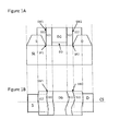
- Figure 1A is a cross-sectional view, across line CS of figure 1B , of one embodiment of the invention at an early stage of manufacture, comprising a substrate layer SL, a source region S and a drain region D, a dummy gate DG, a dummy dielectric DD, a first pair of gate insulating spacers S11 and S12 presenting two lateral side walls SW1 and SW2 in the length direction of the field-effect semiconductor device channel and two outer surface profiles SP1 and SP2 where the lateral side walls meet the substrate layer SL, and a pair of second gate insulating spacers S21 and S22.
- the first gate insulating spacers can be also called first offset spacer or first sacrificial spacers, and are sacrificial spacers laid along the walls of the dummy gate. It shall also be understood that, in the following embodiments, the elements of the figures are shown schematically and for illustration purposes only and therefore the real geometry of those elements may vary when implemented.
- Manufacturing of the field-effect semiconductor device 1 of figure 4 may begin by forming the embodiment of figures 1A and 1B according to the following: in a first step a temporary dummy dielectric DD and a temporary dummy gate DG are formed over a substrate layer SL; in a second step, a pair of temporary first gate insulating spacers S11 and S12 are formed adjacent to the sidewalls of said dummy gate DG and over the substrate layer SL so that the temporary first gate insulating spacers present two lateral side walls SW1 and SW2 and two outer surface profiles SP1 and SP2 where the lateral side walls meet the substrate layer SL; in a third step, a source region S and a drain region D are formed over the substrate layer SL using the surface profiles of said temporary gate insulating spacers lateral side walls; in a fourth step, a pair of second gate insulating spacers S21 and S22 are formed adjacent to the sidewalls of the temporary first gate insulating spacers S11 and S12 and over the source
- the source and drain regions are grown over the substrate layer SL and extend along the temporary first gate insulating spacers lateral side walls surface profiles SP1 and SP2, so that they are aligned to those surface profiles.
- the temporary first gate insulating spacers S11 and S12 limit the source/drain region extension in the direction of the gate.
- the temporary dummy gate DG, the temporary dummy dielectric DD and the temporary first gate insulating spacers S11 and S12 are removed, so as to form a first gate recess space RS1, as shown in figure 2 .
- the temporary first gate insulating spacers S11 and S12 are made of material different from the material of the temporary dummy gate, and the temporary first gate insulating spacers S11 and S12 are removed after having removed that dummy gate. In that case, more definition control over the first gate recess boundaries close to the second gate insulating spacers S21 and S22 is achieved. It shall be understood that the presence of the temporary dummy dielectric DD under the temporary dummy gate structure DG is optional, and that said dummy dielectric DD may be advantageous to achieve better control definition over the first gate recess boundaries close to the substrate layer.
- the temporary first gate insulating spacers S11 and S12 are made of a material which allows removing said first gate spacers without substantially removing the material of the second gate insulating spacers S21 and S22, for example, by etching out the material with a selectivity ratio higher than 2 to 1.
- the temporary first gate insulating spacers are made of an oxide material and the second gate insulating spacers are made of a dense nitride material.
- the temporary first gate insulating spacers are made of a nitride component deposited at temperatures lower than 480 C and designed to etch faster in hydrofluoric acid than the material of the second gate insulating spacers.
- a dielectric layer DL is deposited in the first gate recess space RS1, along the side walls of the second gate sidewall insulating spacers S21 and S22 and over the substrate layer SL, so as to form a second gate recess space RS2.
- the dielectric layer DL is made of a material with high dielectric constant value.
- the thickness of said dielectric layer DL can be precisely controlled using atomic layer deposition (ALD) techniques, and in that sense, according to the embodiment of the invention, said dielectric layer thickness defines the distance from the source/drain junctions to the gate electrode edges, shown as a first distance D1, or underlap distance, in figures 4 , 6 and 12 .
- the field-effect semiconductor device 1 is formed by depositing a gate electrode GE in said second gate recess space RS2.
- Figure 5 is a cross-sectional view of another embodiment of the invention at an early stage of manufacture, comprising a substrate layer SL, a source region S and a drain region D, a dummy gate DG, a dummy dielectric DD, a pair of first gate insulating spacers S11 and S12 presenting two lateral side walls SW1 and SW2 and two outer surface profiles SP1 and SP2 where the lateral side walls meet the substrate layer SL, and a pair of second gate insulating spacers S21 and S22.
- Manufacturing of the field-effect semiconductor device 1 of figure 6 may begin by forming the embodiment of figure 5 according to the following: in a first step a temporary dummy dielectric DD and a temporary dummy gate DG are formed over a substrate layer SL; in a second step, a pair of temporary first gate insulating spacers S11 and S12 are formed adjacent to the sidewalls of said dummy gate DG and over the substrate layer SL so that the temporary first gate insulating spacers present two lateral side walls SW1 and SW2 and two outer surface profiles SP1 and SP2 where the lateral side walls meet the substrate layer SL; in a third step, a source region S and a drain region D are formed in the substrate layer SL using the surface profiles of the temporary gate insulating spacers lateral side walls; in a fourth step, a pair of second gate insulating spacers S21 and S22 are formed adjacent to the sidewalls of the temporary first gate insulating spacers S11 and S12 and over the source and drain regions.
- the source and drain regions are formed in the substrate layer SL and extend along the temporary first gate insulating spacers lateral side walls surface profiles SP1 and SP2.
- the surface profiles of said temporary gate insulating spacers lateral side walls is used as a mask in order to align said source/drain regions, in the substrate layer, to those surface profiles.
- the temporary dummy gate DG, the temporary dummy dielectric DD and the temporary first gate insulating spacers S11 and S12 are removed, so as to form a first gate recess space RS1.
- a dielectric layer DL is deposited in the first gate recess space RS1, along the side walls of the second gate sidewall insulating spacers S21 and S22 and over the substrate layer SL, so as to form a second gate recess space RS2.
- the field-effect semiconductor device 1 is formed by depositing a gate electrode GE in said second gate recess space RS2.
- the embodiment of figure 6 differs from the embodiment of figure 4 in the position of the source and drain regions, but a similar purpose according to the invention is achieved, so as to align the source/drain regions to the surface profiles of the temporary first gate insulating spacers lateral side walls SW1 and SW2 in order to precisely control the underlap distance D1.
- Figure 7 shows a cross-sectional view of another embodiment of the invention at an early stage of manufacture, comprising a substrate layer SL, a dummy gate DG, a dummy dielectric DD and a pair of first gate insulating spacers S11 and S12 presenting two lateral side walls SW1 and SW2 and two outer surface profiles SP1 and SP2 where the lateral side walls meet the substrate layer SL.
- Manufacturing of the field-effect semiconductor device 1 of figure 11 may begin by forming the embodiment of figure 7 according to the following: in a first step, a temporary dummy dielectric DD and a temporary dummy gate DG are formed over a substrate layer SL; in a second step, a pair of temporary first gate insulating spacers S11 and S12 are formed adjacent to the sidewalls of said dummy gate DG and over the substrate layer SL so that the temporary first gate insulating spacers present two lateral side walls SW1 and SW2 and two outer surface profiles SP1 and SP2 where the lateral side walls meet the substrate layer SL.
- an opening extending from the surface profiles SP1 and SP2 to a predetermined distance OD in the direction of the dummy gate DG, is formed in the substrate layer SL, as shown in figure 8 , and the opening follows or presents the same surface profile of the temporary first gate insulating spacers lateral side walls surface profile SP1 and SP2 under the dummy gate DG (when seen from a top view of the FET device).
- the openings are filled so as to form a source region S and a drain region D in the substrate layer SL.
- a pair of second gate insulating spacers S21 and S22 are formed adjacent to the sidewalls of the temporary first gate insulating spacers S11 and S12 and over the source and drain regions.
- the temporary dummy gate DG, the temporary dummy dielectric DD and the temporary first gate insulating spacers S11 and S12 are removed, so as to form a first gate recess space RS1.
- a dielectric layer DL is deposited in the first gate recess space RS1, along the side walls of the second gate sidewall insulating spacers S21 and S22 and over the substrate layer SL, so as to form a second gate recess space RS2.
- the field-effect semiconductor device 1 of figure 11 according to one embodiment of the invention is formed by depositing a gate electrode GE in said second gate recess space RS2.
- the source and drain regions extend to a predetermined distance, OD in figure 8 , from an early defined surface profile SP1 and SP2 of the temporary first gate insulating spacers lateral side walls towards the gate electrode GE, and the source and drain regions follow the surface profile of the temporary first gate insulating spacers lateral side walls SW1 and SW2 under the gate electrode.
- both the thickness of the dielectric layer DL and the extension of the source/drain regions can be precisely controlled, both parameters can be used to precisely control a distance from the source/drain junctions under the gate electrode to the gate electrode edges, shown as a second distance D2, or overlap distance, in figures 11 and 12 .
- Figure 12 shows a cross-sectional view of another embodiment of a field-effect semiconductor device 1 according to the invention at a final stage of manufacture, comprising a substrate layer SL, a first and a second source regions S1 and S2, a first and a second drain regions D1 and D2, a dielectric layer DL, a gate electrode GE and a pair of second gate insulating spacers S21 and S22.
- figure 12 is manufactured similarly to the embodiment shown in figure 11 , but further comprising second source and drain regions formed over the substrate layer which are aligned using a surface profile of the temporary gate insulating spacers lateral side walls SW1 and SW2 similarly to the embodiment shown in figure 4 .
- Figure 13 is a simplified and schematic 3D view of a non-planar field-effect semiconductor device, such as FinFET, according to one embodiment of the invention, at an early stage of manufacture, comprising a FIN substrate layer SL, a source region S and a drain region D formed in said FIN substrate layer, a dummy gate DG, a first pair of gate insulating spacers S11 and S12 presenting two lateral side walls SW1 and SW2 in the length direction of the field-effect semiconductor device channel and two outer surface profiles SP1 and SP2 (along 3 FIN walls: front, top and back walls, as shown in the figure) where the temporary first gate insulating spacers lateral side walls SW1 and SW2 meet the FIN substrate layer SL.
- the embodiment shown in the figure is similar to the planar embodiment of figure 5 but at a stage previous to forming the second gate insulating spacers S21 and S22.
Abstract
The invention relates to a method for manufacturing a field-effect semiconductor device (1), the method comprising: forming a temporary dummy gate (DG) over a substrate layer (SL); forming temporary first gate insulating spacers (S11, S12) adjacent to the sidewalls of said dummy gate (DG) and over the substrate layer (SL), the temporary first gate insulating spacers comprising two lateral side walls (SW1, SW2) and presenting two outer surface profiles (SP1, SP2) where said lateral side walls meet said substrate layer (SL); forming a source region (S) and a drain region (D) in and/or over the substrate layer (SL) using said temporary first gate insulating spacers lateral side walls surface profiles (SP1, SP2); forming second gate insulating spacers (S21, S22) adjacent to the sidewalls of the temporary first gate insulating spacers (S11, S12) and over the source and drain regions (S, D); removing the temporary dummy gate (DG) and the temporary first gate insulating spacers (S11, S12), thereby forming a first gate recess space (RS1); depositing a dielectric layer (DL) in said first gate recess space (RS1), along the side walls of the second gate sidewall insulating spacers (S21, S22) and over the substrate layer (SL), thereby forming a second gate recess space (RS2); and depositing a gate electrode (GE) in the second gate recess space (RS2).
The invention also relates to a field-effect semiconductor device and associated products, e.g. integrated or electronic circuits comprising one or a plurality of said FET devices manufactured according to the method described herein.
Description
- The present invention relates generally to field-effect semiconductor devices, such as field-effect transistors (FETs), and more specifically to a method for manufacturing a field effect semiconductor device following a replacement gate process.
- Several challenges still remain for large scale integration of field-effect semiconductor devices. As FET transistor gate lengths continue to scale down, the offset spacer design becomes critical for transistor performance. The required dimensions of such dielectric offset spacers, also referred to as sidewall spacers, are increasingly smaller and the processes to define the offset spacer profile are increasingly difficult to control in order to achieve the desired critical dimensions.
- Therefore there is a need to address the heightened sensitivity to gate spacer dimensioning using process techniques for gate sidewall spacer formation, particularly in manufacturing processes following a gate-last approach, also called replacement gate or damascene gate processes.
- US patent application, for example,
2007/0287259 A1 discloses the use of gate isolation spacers in a method of forming a semiconductor structure according to a replacement gate process. - Also, in
US patent application 2006/0148182 A1 , a self-aligned source drain quantum well transistor or high electron mobility transistor is formed using a replacement metal gate process, in which sidewall spacers temporarily bracket a dummy gate electrode. - A problem with the current techniques for manufacturing FET devices is that they lack a precise control of the distance from the source/drain extensions to the gate edge.
- It is the object of the present invention to provide an improved FET device and method for manufacturing the same, using a replacement gate process, which overcomes current FET design source/drain extension underlap and overlap drawbacks.
- According to one aspect of the present invention, a method for manufacturing a field-effect semiconductor device is provided, the method comprising: forming a temporary dummy gate over a substrate layer; forming temporary first gate insulating spacers adjacent to the sidewalls of said dummy gate and over the substrate layer, the temporary first gate insulating spacers comprising two lateral side walls and presenting two outer surface profiles where said lateral side walls meet said substrate layer; forming a source region and a drain region in and/or over the substrate layer using said temporary first gate insulating spacers lateral side walls surface profiles; forming second gate insulating spacers adjacent to the sidewalls of said temporary first gate insulating spacers and over the source and drain regions; removing the temporary dummy gate and the temporary first gate insulating spacers, thereby forming a first gate recess space; depositing a dielectric layer in said first gate recess space, directly along the side walls of the second gate sidewall insulating spacers and over the substrate layer, thereby forming a second gate recess space; and depositing a gate electrode in said second gate recess space.
- Advantageously field-effect semiconductor devices manufactured according to the invention avoid sensitivity to offset spacer critical dimension and present reduced sensitivity towards S/D-gate overlap/underlap variations, which greatly impact the transistor performance.
- Advantageously, the method for manufacturing a field-effect semiconductor device according to the invention allows better control and design of the device performance characteristics (e.g. resistance, capacitance and gate-drain leakage) by providing a mechanism to increase precision control for defining the source and drain region distance to the gate electrode edges, e.g. for both overlap and underlap field-effect semiconductor device design. In that sense, the method according to the invention advantageously allows better repeatability of the field-effect semiconductor device performance characteristics.
- The method according to the invention can be advantageously applied for manufacturing both planar devices, such as, for example, implant-free quantum well (IFQW) FET devices or silicon on oxide (SOI) pFET devices, and non-planar FET devices such as, for example, FinFET devices. Advantageously, in case of non-planar devices, the S/D-gate overlap/underlap distance along the FIN walls is more precisely controlled, and for example, a fixed external resistance (Rext) along the FIN walls is achieved.
- According to another aspect of the invention the step of forming the source and drain region comprises using the surface profiles of the temporary first gate insulating spacers lateral side walls to align the source/drain regions, in or over the substrate layer, to those surface profiles.
- According to still another aspect of the invention, the step of forming the source and drain region comprises using the surface profiles of the temporary first gate insulating spacers lateral side walls to define said source/drain region extension, in the substrate layer, under the dummy gate.
- Advantageously, according to the invention, the surface profile of the temporary first gate insulating spacers lateral side walls is set and used as a reference point to align the source/drain regions over the substrate layer, e.g. by epitaxial overgrowth of the source/drain regions, or as a mask to align the source/drain regions in the substrate layer, or to define the source/drain region extension in the substrate under the dummy gate by, for example, first etching the substrate layer starting from the surface profile of said temporary first gate insulating spacers lateral side walls and then filling said etched openings to form the source/drain regions.
- According to still another aspect of the invention, the step of forming the source and drain region comprises using said surface profiles of said temporary first gate insulating spacers lateral side walls to align said source/drain regions, over the substrate layer, to said surface profiles and to define said source/drain region extension, in the substrate layer, under the dummy gate.
- According to one embodiment of the invention, the temporary first gate insulating spacers are removed after the temporary dummy gate removal, thereby forming a first gate recess space.
- According to another embodiment of the invention, the method comprises forming a temporary dummy dielectric between the dummy gate and the substrate layer, and the step of removing the temporary dummy gate and the temporary first gate insulating spacers comprises also removing the dummy dielectric, thereby forming the first gate recess space.
- According to one embodiment of the invention, the step of removing the temporary first gate insulating spacers comprises selectively removing the material of the temporary first gate insulating spacers without substantially removing the material of the second gate insulating spacers, for example by etching out the material of the temporary first gate insulating spacers without substantially removing the material of the second gate insulating spacers, e.g. with a selectivity ratio higher than 2 to 1. In one example, the temporary first gate insulating spacers are made of an oxide material and the second gate insulating spacers are made of a dense nitride material. In another example, the temporary first gate insulating spacers are made of a nitride component deposited at temperatures lower than 480 C and designed to etch faster in hydrofluoric acid than the material of the second gate insulating spacers.
- According to another embodiment of the invention, the substrate layer comprises at least one silicon wafer layer, at least a silicon wafer layer and a quantum well layer, or at least a silicon wafer layer, a buried oxide layer and a silicon layer.
- The invention also relates to field-effect semiconductor devices and associated devices, e.g. integrated or electronic circuits comprising one or a plurality of said FET devices manufactured according to the method described herein.
- Certain objects and advantages of various inventive aspects have been described above. It is to be understood that not necessarily all such objects or advantages may be achieved in accordance with any particular embodiment of the invention. Those skilled in the art will recognize that the invention may be embodied or carried out in a manner that achieves or optimizes one advantage or group of advantages without necessarily achieving other objects or advantages as may be taught or suggested herein.
- The above and other aspects of the invention will be apparent from the following description and with reference to the non-restrictive example embodiment(s) described hereinafter.
-
Figure 1A is a cross-sectional view of one embodiment of the invention at an early stage of manufacture. -
Figure 1B is a top view of the embodiment shown infigure 1A . -
Figure 2 is a cross-sectional view of the embodiment shown infigure 1A in a subsequent step of manufacture in accordance with the invention. -
Figure 3 is a cross-sectional view of the embodiment shown infigure 2 in a subsequent step of manufacture in accordance with the invention. -
Figure 4 is a cross-sectional view of one embodiment of a field-effect semiconductor device according to the invention after completion of the gate stack stage of manufacture comprising the manufacturing steps shown infigures 1 to 3 . -
Figure 5 is a cross-sectional view of another embodiment of the invention at an early stage of manufacture. -
Figure 6 is a cross-sectional view of one embodiment of a field-effect semiconductor device according to the invention after completion of the gate stack stage of manufacture comprising the manufacturing step offigure 5 . -
Figure 7 is a cross-sectional view of still another embodiment of the invention at an early stage of manufacture. -
Figure 8 is a cross-sectional view of the embodiment shown infigure 7 in a subsequent step of manufacture in accordance with the invention. -
Figure 9 is a cross-sectional view of the embodiment shown infigure 8 in a subsequent step of manufacture in accordance with the invention. -
Figure 10 is a cross-sectional view of the embodiment shown infigure 9 in a subsequent step of manufacture in accordance with the invention. -
Figure 11 is a cross-sectional view of one embodiment of a field-effect semiconductor device according to the invention after completion of the gate stack stage of manufacture comprising the manufacturing steps shown infigures 7 to 10 . -
Figure 12 is a cross-sectional view of one embodiment of a field-effect semiconductor device according to the invention after completion of the gate stack stage of manufacture. -
Figure 13 is a schematic 3D view of a non-planar field-effect semiconductor device at an early stage of manufacture according to an exemplary embodiment of invention. - In the following, it should be appreciated that in the description of exemplary embodiments of the invention, various features of the invention are sometimes grouped together in a single embodiment, figure, or description thereof for the purpose of streamlining the disclosure and aiding in the understanding of one or more of the various inventive aspects. This is however not to be interpreted as the invention requiring more features than the ones expressly recited in each claim, with each claim standing on its own as a separate embodiment of this invention.
- Furthermore, while some embodiments described herein include some but not other features included in other embodiments, combinations of features of different embodiments are meant to be within the scope of the invention, and form different embodiments, as would be understood by those skilled in the art. In the description of the embodiments, numerous specific details are set forth.
- However, it is understood that embodiments of the invention may be practiced without these non-essential specific details. In other instances, well-known methods, structures and techniques have not been shown in detail in order not to obscure an understanding of this description.
-
Figure 1A is a cross-sectional view, across line CS offigure 1B , of one embodiment of the invention at an early stage of manufacture, comprising a substrate layer SL, a source region S and a drain region D, a dummy gate DG, a dummy dielectric DD, a first pair of gate insulating spacers S11 and S12 presenting two lateral side walls SW1 and SW2 in the length direction of the field-effect semiconductor device channel and two outer surface profiles SP1 and SP2 where the lateral side walls meet the substrate layer SL, and a pair of second gate insulating spacers S21 and S22. - The first gate insulating spacers can be also called first offset spacer or first sacrificial spacers, and are sacrificial spacers laid along the walls of the dummy gate. It shall also be understood that, in the following embodiments, the elements of the figures are shown schematically and for illustration purposes only and therefore the real geometry of those elements may vary when implemented.
- Manufacturing of the field-
effect semiconductor device 1 offigure 4 may begin by forming the embodiment offigures 1A and 1B according to the following: in a first step a temporary dummy dielectric DD and a temporary dummy gate DG are formed over a substrate layer SL; in a second step, a pair of temporary first gate insulating spacers S11 and S12 are formed adjacent to the sidewalls of said dummy gate DG and over the substrate layer SL so that the temporary first gate insulating spacers present two lateral side walls SW1 and SW2 and two outer surface profiles SP1 and SP2 where the lateral side walls meet the substrate layer SL; in a third step, a source region S and a drain region D are formed over the substrate layer SL using the surface profiles of said temporary gate insulating spacers lateral side walls; in a fourth step, a pair of second gate insulating spacers S21 and S22 are formed adjacent to the sidewalls of the temporary first gate insulating spacers S11 and S12 and over the source and drain regions. - According to one embodiment of the invention, as shown in
figures 1A and 1B , the source and drain regions are grown over the substrate layer SL and extend along the temporary first gate insulating spacers lateral side walls surface profiles SP1 and SP2, so that they are aligned to those surface profiles. According to the embodiment of the invention, the temporary first gate insulating spacers S11 and S12 limit the source/drain region extension in the direction of the gate. - In subsequent steps of manufacture of the field-
effect semiconductor device 1 offigure 4 , the temporary dummy gate DG, the temporary dummy dielectric DD and the temporary first gate insulating spacers S11 and S12 are removed, so as to form a first gate recess space RS1, as shown infigure 2 . - In a preferred embodiment according to the invention, the temporary first gate insulating spacers S11 and S12 are made of material different from the material of the temporary dummy gate, and the temporary first gate insulating spacers S11 and S12 are removed after having removed that dummy gate. In that case, more definition control over the first gate recess boundaries close to the second gate insulating spacers S21 and S22 is achieved. It shall be understood that the presence of the temporary dummy dielectric DD under the temporary dummy gate structure DG is optional, and that said dummy dielectric DD may be advantageous to achieve better control definition over the first gate recess boundaries close to the substrate layer. According to another preferred embodiment of the invention, the temporary first gate insulating spacers S11 and S12 are made of a material which allows removing said first gate spacers without substantially removing the material of the second gate insulating spacers S21 and S22, for example, by etching out the material with a selectivity ratio higher than 2 to 1. In one example, the temporary first gate insulating spacers are made of an oxide material and the second gate insulating spacers are made of a dense nitride material. In another example, the temporary first gate insulating spacers are made of a nitride component deposited at temperatures lower than 480 C and designed to etch faster in hydrofluoric acid than the material of the second gate insulating spacers.
- Now referring to the
figure 3 , which shows an embodiment in a subsequent step of manufacture of the field-effect semiconductor device 1 offigure 4 , a dielectric layer DL is deposited in the first gate recess space RS1, along the side walls of the second gate sidewall insulating spacers S21 and S22 and over the substrate layer SL, so as to form a second gate recess space RS2. - According to a preferred embodiment of the invention, the dielectric layer DL is made of a material with high dielectric constant value. Advantageously, the thickness of said dielectric layer DL can be precisely controlled using atomic layer deposition (ALD) techniques, and in that sense, according to the embodiment of the invention, said dielectric layer thickness defines the distance from the source/drain junctions to the gate electrode edges, shown as a first distance D1, or underlap distance, in
figures 4 ,6 and12 . - Finally, in
figure 4 , the field-effect semiconductor device 1 according to one embodiment of the invention is formed by depositing a gate electrode GE in said second gate recess space RS2. -
Figure 5 is a cross-sectional view of another embodiment of the invention at an early stage of manufacture, comprising a substrate layer SL, a source region S and a drain region D, a dummy gate DG, a dummy dielectric DD, a pair of first gate insulating spacers S11 and S12 presenting two lateral side walls SW1 and SW2 and two outer surface profiles SP1 and SP2 where the lateral side walls meet the substrate layer SL, and a pair of second gate insulating spacers S21 and S22. - Manufacturing of the field-
effect semiconductor device 1 offigure 6 may begin by forming the embodiment offigure 5 according to the following: in a first step a temporary dummy dielectric DD and a temporary dummy gate DG are formed over a substrate layer SL; in a second step, a pair of temporary first gate insulating spacers S11 and S12 are formed adjacent to the sidewalls of said dummy gate DG and over the substrate layer SL so that the temporary first gate insulating spacers present two lateral side walls SW1 and SW2 and two outer surface profiles SP1 and SP2 where the lateral side walls meet the substrate layer SL; in a third step, a source region S and a drain region D are formed in the substrate layer SL using the surface profiles of the temporary gate insulating spacers lateral side walls; in a fourth step, a pair of second gate insulating spacers S21 and S22 are formed adjacent to the sidewalls of the temporary first gate insulating spacers S11 and S12 and over the source and drain regions. - According to one embodiment of the invention, as shown in
figure 5 , the source and drain regions are formed in the substrate layer SL and extend along the temporary first gate insulating spacers lateral side walls surface profiles SP1 and SP2. In order to form said source/drain regions, for example, the surface profiles of said temporary gate insulating spacers lateral side walls is used as a mask in order to align said source/drain regions, in the substrate layer, to those surface profiles. - Similarly to the embodiment of
figure 2 , in subsequent steps of manufacture of the field-effect semiconductor device 1 offigure 6 , the temporary dummy gate DG, the temporary dummy dielectric DD and the temporary first gate insulating spacers S11 and S12 are removed, so as to form a first gate recess space RS1. - Also similarly to the embodiment shown in
figure 3 , in a subsequent step of manufacture of the field-effect semiconductor device 1 offigure 6 , a dielectric layer DL is deposited in the first gate recess space RS1, along the side walls of the second gate sidewall insulating spacers S21 and S22 and over the substrate layer SL, so as to form a second gate recess space RS2. - Finally, as shown in
figure 6 , the field-effect semiconductor device 1 according to one embodiment of the invention is formed by depositing a gate electrode GE in said second gate recess space RS2. - It shall be understood that the embodiment of
figure 6 differs from the embodiment offigure 4 in the position of the source and drain regions, but a similar purpose according to the invention is achieved, so as to align the source/drain regions to the surface profiles of the temporary first gate insulating spacers lateral side walls SW1 and SW2 in order to precisely control the underlap distance D1. -
Figure 7 shows a cross-sectional view of another embodiment of the invention at an early stage of manufacture, comprising a substrate layer SL, a dummy gate DG, a dummy dielectric DD and a pair of first gate insulating spacers S11 and S12 presenting two lateral side walls SW1 and SW2 and two outer surface profiles SP1 and SP2 where the lateral side walls meet the substrate layer SL. - Manufacturing of the field-
effect semiconductor device 1 offigure 11 may begin by forming the embodiment offigure 7 according to the following: in a first step, a temporary dummy dielectric DD and a temporary dummy gate DG are formed over a substrate layer SL; in a second step, a pair of temporary first gate insulating spacers S11 and S12 are formed adjacent to the sidewalls of said dummy gate DG and over the substrate layer SL so that the temporary first gate insulating spacers present two lateral side walls SW1 and SW2 and two outer surface profiles SP1 and SP2 where the lateral side walls meet the substrate layer SL. - In subsequent steps of manufacture of the field-
effect semiconductor device 1 offigure 11 , an opening, extending from the surface profiles SP1 and SP2 to a predetermined distance OD in the direction of the dummy gate DG, is formed in the substrate layer SL, as shown infigure 8 , and the opening follows or presents the same surface profile of the temporary first gate insulating spacers lateral side walls surface profile SP1 and SP2 under the dummy gate DG (when seen from a top view of the FET device). - Referring next to the
figure 9 , which shows an embodiment in a subsequent step of manufacture of the field-effect semiconductor device 1 offigure 11 , the openings are filled so as to form a source region S and a drain region D in the substrate layer SL. Then, infigure 10 , a pair of second gate insulating spacers S21 and S22 are formed adjacent to the sidewalls of the temporary first gate insulating spacers S11 and S12 and over the source and drain regions. - Similarly to the embodiment of
figure 2 , in subsequent steps of manufacture of the field-effect semiconductor device 1 offigure 11 , the temporary dummy gate DG, the temporary dummy dielectric DD and the temporary first gate insulating spacers S11 and S12 are removed, so as to form a first gate recess space RS1. - Also similarly to the embodiment shown in
figure 3 , in a subsequent step of manufacture of the field-effect semiconductor device 1 offigure 11 , a dielectric layer DL is deposited in the first gate recess space RS1, along the side walls of the second gate sidewall insulating spacers S21 and S22 and over the substrate layer SL, so as to form a second gate recess space RS2. Then, in a final step, the field-effect semiconductor device 1 offigure 11 according to one embodiment of the invention is formed by depositing a gate electrode GE in said second gate recess space RS2. - According to an embodiment of the invention, as shown in
figure 11 , the source and drain regions extend to a predetermined distance, OD infigure 8 , from an early defined surface profile SP1 and SP2 of the temporary first gate insulating spacers lateral side walls towards the gate electrode GE, and the source and drain regions follow the surface profile of the temporary first gate insulating spacers lateral side walls SW1 and SW2 under the gate electrode. Advantageously, since both the thickness of the dielectric layer DL and the extension of the source/drain regions can be precisely controlled, both parameters can be used to precisely control a distance from the source/drain junctions under the gate electrode to the gate electrode edges, shown as a second distance D2, or overlap distance, infigures 11 and12 . -
Figure 12 shows a cross-sectional view of another embodiment of a field-effect semiconductor device 1 according to the invention at a final stage of manufacture, comprising a substrate layer SL, a first and a second source regions S1 and S2, a first and a second drain regions D1 and D2, a dielectric layer DL, a gate electrode GE and a pair of second gate insulating spacers S21 and S22. - It is understood by the person skilled in the art that the embodiment of
figure 12 is manufactured similarly to the embodiment shown infigure 11 , but further comprising second source and drain regions formed over the substrate layer which are aligned using a surface profile of the temporary gate insulating spacers lateral side walls SW1 and SW2 similarly to the embodiment shown infigure 4 . -
Figure 13 is a simplified and schematic 3D view of a non-planar field-effect semiconductor device, such as FinFET, according to one embodiment of the invention, at an early stage of manufacture, comprising a FIN substrate layer SL, a source region S and a drain region D formed in said FIN substrate layer, a dummy gate DG, a first pair of gate insulating spacers S11 and S12 presenting two lateral side walls SW1 and SW2 in the length direction of the field-effect semiconductor device channel and two outer surface profiles SP1 and SP2 (along 3 FIN walls: front, top and back walls, as shown in the figure) where the temporary first gate insulating spacers lateral side walls SW1 and SW2 meet the FIN substrate layer SL. The embodiment shown in the figure is similar to the planar embodiment offigure 5 but at a stage previous to forming the second gate insulating spacers S21 and S22. - It shall be understood that the person skilled in the art will readily be able to advantageously apply the aspects of the invention described hereinabove in a non-planar implementation of a FET device, in order to precisely control the source/drain-gate overlap/underlap distance along the FIN walls.
Claims (10)
- A method for manufacturing a field-effect semiconductor device (1) comprising:- forming a temporary dummy gate (DG) over a substrate layer (SL);- forming temporary first gate insulating spacers (S11, S12) adjacent to the sidewalls of said dummy gate (DG) and over the substrate layer (SL), the temporary first gate insulating spacers comprising two lateral side walls (SW1, SW2) and presenting two outer surface profiles (SP1, SP2) where said lateral side walls meet said substrate layer (SL);- forming a source region (S) and a drain region (D) in and/or over the substrate layer (SL) using said temporary first gate insulating spacers lateral side walls surface profiles (SP1, SP2);- forming second gate insulating spacers (S21, S22) adjacent to the sidewalls of said temporary first gate insulating spacers (S11, S12) and over the source and drain regions (S, D);- removing the temporary dummy gate (DG) and the temporary first gate insulating spacers (S11, S12), thereby forming a first gate recess space (RS1);- depositing a dielectric layer (DL) in said first gate recess space (RS1), along the side walls of the second gate sidewall insulating spacers (S21, S22) and over the substrate layer (SL), thereby forming a second gate recess space (RS2); and- depositing a gate electrode (GE) in said second gate recess space (RS2).
- The method according to claim 1 wherein the step of forming a source region (S) and a drain region (D) comprises using said surface profiles (SP1, SP2) of said temporary first gate insulating spacers lateral side walls (SW1, SW2) to align said source/drain regions, in or over the substrate layer, to said surface profiles.
- The method according to claim 1 wherein the step of forming a source region (S) and a drain region (D) comprises using said surface profiles (SP1, SP2) of said temporary first gate insulating spacers lateral side walls (SW1, SW2) to define said source/drain region extension, in the substrate layer, under the dummy gate (DG).
- The method according to claim 1 wherein the step of forming a source region (S) and a drain region (D) comprises using said surface profiles (SP1, SP2) of said temporary first gate insulating spacers lateral side walls (SW1, SW2) to align said source/drain regions, over the substrate layer, to said surface profiles and to define said source/drain region extension, in the substrate layer, under the dummy gate (DG).
- The method according to any of the preceding claims wherein the temporary first gate insulating spacers (S11, S12) are removed after the temporary dummy gate removal, thereby forming a first gate recess space (RS1);
- The method according to any of the preceding claims further comprising forming a temporary dummy dielectric (DD) between the dummy gate (DG) and the substrate layer (SL), and wherein the step of removing the temporary dummy gate (DG) and the temporary first gate insulating spacers (S11, S12) comprises also removing the dummy dielectric (DD), thereby forming the first gate recess space (RS1).
- The method according to any of the preceding claims wherein the step of removing the temporary first gate insulating spacers (S11, S12) comprises selectively removing the material of the temporary first gate insulating spacers without substantially removing the material of the second gate insulating spacers (S21, S22).
- The method according to claim 7 wherein the temporary first gate insulating spacers (S11, S12) are made of an oxide material and the second gate insulating spacers (S21, S22) are made of a dense nitride material.
- The method according to claim 7 wherein the temporary first gate insulating spacers (S11, S12) are made of a nitride component deposited at temperatures lower than 480 C and designed to etch faster in hydrofluoric acid than the material of the second gate insulating spacers (S21, S22).
- The method according to any of the previous claims wherein the substrate layer (SL) comprises at least one silicon wafer layer; or at least a silicon wafer layer and a quantum well layer; or at least a silicon wafer layer, a buried oxide layer and a silicon layer.
Priority Applications (1)
| Application Number | Priority Date | Filing Date | Title |
|---|---|---|---|
| EP12199358.8A EP2608264A1 (en) | 2011-12-23 | 2012-12-24 | Method for manufacturing a field-effect semiconductor device following a replacement gate process |
Applications Claiming Priority (2)
| Application Number | Priority Date | Filing Date | Title |
|---|---|---|---|
| EP11195617 | 2011-12-23 | ||
| EP12199358.8A EP2608264A1 (en) | 2011-12-23 | 2012-12-24 | Method for manufacturing a field-effect semiconductor device following a replacement gate process |
Publications (1)
| Publication Number | Publication Date |
|---|---|
| EP2608264A1 true EP2608264A1 (en) | 2013-06-26 |
Family
ID=47469795
Family Applications (1)
| Application Number | Title | Priority Date | Filing Date |
|---|---|---|---|
| EP12199358.8A Withdrawn EP2608264A1 (en) | 2011-12-23 | 2012-12-24 | Method for manufacturing a field-effect semiconductor device following a replacement gate process |
Country Status (3)
| Country | Link |
|---|---|
| US (1) | US20130181301A1 (en) |
| EP (1) | EP2608264A1 (en) |
| JP (1) | JP2013138201A (en) |
Families Citing this family (5)
| Publication number | Priority date | Publication date | Assignee | Title |
|---|---|---|---|---|
| US9318607B2 (en) * | 2013-07-12 | 2016-04-19 | Samsung Electronics Co., Ltd. | Semiconductor device and method of fabricating the same |
| CN104576376A (en) * | 2013-10-13 | 2015-04-29 | 中国科学院微电子研究所 | Mosfet structure and manufacturing method thereof |
| US9373641B2 (en) | 2014-08-19 | 2016-06-21 | International Business Machines Corporation | Methods of forming field effect transistors using a gate cut process following final gate formation |
| US9812323B2 (en) * | 2014-09-08 | 2017-11-07 | Internaitonal Business Machines Corporation | Low external resistance channels in III-V semiconductor devices |
| US11387338B1 (en) * | 2021-01-22 | 2022-07-12 | Applied Materials, Inc. | Methods for forming planar metal-oxide-semiconductor field-effect transistors |
Citations (7)
| Publication number | Priority date | Publication date | Assignee | Title |
|---|---|---|---|---|
| US6054355A (en) * | 1997-06-30 | 2000-04-25 | Kabushiki Kaisha Toshiba | Method of manufacturing a semiconductor device which includes forming a dummy gate |
| US20060068590A1 (en) * | 2004-09-29 | 2006-03-30 | Nick Lindert | Metal gate transistors with epitaxial source and drain regions |
| US20060091432A1 (en) * | 2004-11-02 | 2006-05-04 | International Business Machines Corporation | Damascene gate field effect transistor with an internal spacer structure |
| US20060148182A1 (en) | 2005-01-03 | 2006-07-06 | Suman Datta | Quantum well transistor using high dielectric constant dielectric layer |
| US20070287259A1 (en) | 2006-06-08 | 2007-12-13 | Kavalieros Jack T | Forming ultra-shallow junctions |
| US20100001323A1 (en) * | 2006-12-11 | 2010-01-07 | Sony Corporation | Method for manufacturing semiconductor device and semiconductor device |
| US20110042758A1 (en) * | 2009-08-24 | 2011-02-24 | Sony Corporation | Semiconductor device and manufacturing method thereof |
-
2012
- 2012-12-19 JP JP2012277194A patent/JP2013138201A/en active Pending
- 2012-12-21 US US13/725,587 patent/US20130181301A1/en not_active Abandoned
- 2012-12-24 EP EP12199358.8A patent/EP2608264A1/en not_active Withdrawn
Patent Citations (7)
| Publication number | Priority date | Publication date | Assignee | Title |
|---|---|---|---|---|
| US6054355A (en) * | 1997-06-30 | 2000-04-25 | Kabushiki Kaisha Toshiba | Method of manufacturing a semiconductor device which includes forming a dummy gate |
| US20060068590A1 (en) * | 2004-09-29 | 2006-03-30 | Nick Lindert | Metal gate transistors with epitaxial source and drain regions |
| US20060091432A1 (en) * | 2004-11-02 | 2006-05-04 | International Business Machines Corporation | Damascene gate field effect transistor with an internal spacer structure |
| US20060148182A1 (en) | 2005-01-03 | 2006-07-06 | Suman Datta | Quantum well transistor using high dielectric constant dielectric layer |
| US20070287259A1 (en) | 2006-06-08 | 2007-12-13 | Kavalieros Jack T | Forming ultra-shallow junctions |
| US20100001323A1 (en) * | 2006-12-11 | 2010-01-07 | Sony Corporation | Method for manufacturing semiconductor device and semiconductor device |
| US20110042758A1 (en) * | 2009-08-24 | 2011-02-24 | Sony Corporation | Semiconductor device and manufacturing method thereof |
Also Published As
| Publication number | Publication date |
|---|---|
| JP2013138201A (en) | 2013-07-11 |
| US20130181301A1 (en) | 2013-07-18 |
Similar Documents
| Publication | Publication Date | Title |
|---|---|---|
| US9799748B1 (en) | Method of forming inner spacers on a nano-sheet/wire device | |
| KR101729439B1 (en) | Finfet with buried insulator layer and method for forming | |
| US8728885B1 (en) | Methods of forming a three-dimensional semiconductor device with a nanowire channel structure | |
| US8617937B2 (en) | Forming narrow fins for finFET devices using asymmetrically spaced mandrels | |
| EP3312876A1 (en) | Finfet device and fabrication method thereof | |
| US10535771B1 (en) | Method for forming replacement air gap | |
| US9704990B1 (en) | Vertical FET with strained channel | |
| US9318575B2 (en) | Semiconductor device and method for fabricating the same | |
| US20150333145A1 (en) | High density finfet devices with unmerged fins | |
| US9117805B2 (en) | Air-spacer MOS transistor | |
| JP6173083B2 (en) | Method for manufacturing a field effect semiconductor device | |
| EP2608264A1 (en) | Method for manufacturing a field-effect semiconductor device following a replacement gate process | |
| US20140159124A1 (en) | Epitaxial grown extremely shallow extension region | |
| US20100308409A1 (en) | Finfet structures with fins having stress-inducing caps and methods for fabricating the same | |
| US20150325436A1 (en) | Semiconductor devices including an electrically-decoupled fin and methods of forming the same | |
| US9472654B2 (en) | Forming low parasitic trim gate last MOSFET | |
| US9793378B2 (en) | Fin field effect transistor device with reduced overlap capacitance and enhanced mechanical stability | |
| US9209269B2 (en) | Semiconductor structure and method for manufacturing the same | |
| US20180108732A1 (en) | Notched fin structures and methods of manufacture | |
| US20140235043A1 (en) | Method for forming fin-shaped structure | |
| CN105679674A (en) | Method for reducing gate height variation due to overlapping masks | |
| US9570588B2 (en) | Methods of forming transistor structures including forming channel material after formation processes to prevent damage to the channel material | |
| US9530841B1 (en) | Gate-all-around nanowire field-effect transistor device | |
| US8618616B2 (en) | FinFET structures and methods for fabricating the same | |
| CN102222693B (en) | FinFET device and manufacturing method thereof |
Legal Events
| Date | Code | Title | Description |
|---|---|---|---|
| AK | Designated contracting states |
Kind code of ref document: A1 Designated state(s): AL AT BE BG CH CY CZ DE DK EE ES FI FR GB GR HR HU IE IS IT LI LT LU LV MC MK MT NL NO PL PT RO RS SE SI SK SM TR |
|
| AX | Request for extension of the european patent |
Extension state: BA ME |
|
| PUAI | Public reference made under article 153(3) epc to a published international application that has entered the european phase |
Free format text: ORIGINAL CODE: 0009012 |
|
| STAA | Information on the status of an ep patent application or granted ep patent |
Free format text: STATUS: THE APPLICATION IS DEEMED TO BE WITHDRAWN |
|
| 18D | Application deemed to be withdrawn |
Effective date: 20140103 |