EP1944794A1 - A method for controlled formation of a gate dielectric stack - Google Patents
A method for controlled formation of a gate dielectric stack Download PDFInfo
- Publication number
- EP1944794A1 EP1944794A1 EP07113225A EP07113225A EP1944794A1 EP 1944794 A1 EP1944794 A1 EP 1944794A1 EP 07113225 A EP07113225 A EP 07113225A EP 07113225 A EP07113225 A EP 07113225A EP 1944794 A1 EP1944794 A1 EP 1944794A1
- Authority
- EP
- European Patent Office
- Prior art keywords
- layer
- reo
- cdm
- forming
- deposited
- Prior art date
- Legal status (The legal status is an assumption and is not a legal conclusion. Google has not performed a legal analysis and makes no representation as to the accuracy of the status listed.)
- Withdrawn
Links
- 238000000034 method Methods 0.000 title claims abstract description 64
- 230000015572 biosynthetic process Effects 0.000 title description 18
- 239000004065 semiconductor Substances 0.000 claims abstract description 15
- VYPSYNLAJGMNEJ-UHFFFAOYSA-N silicon dioxide Inorganic materials O=[Si]=O VYPSYNLAJGMNEJ-UHFFFAOYSA-N 0.000 claims description 111
- 229910001404 rare earth metal oxide Inorganic materials 0.000 claims description 91
- 229910052761 rare earth metal Inorganic materials 0.000 claims description 62
- 229910052751 metal Inorganic materials 0.000 claims description 58
- 239000002184 metal Substances 0.000 claims description 58
- 229910052681 coesite Inorganic materials 0.000 claims description 54
- 229910052906 cristobalite Inorganic materials 0.000 claims description 54
- 239000000377 silicon dioxide Substances 0.000 claims description 54
- 229910052682 stishovite Inorganic materials 0.000 claims description 54
- 229910052905 tridymite Inorganic materials 0.000 claims description 54
- 238000000137 annealing Methods 0.000 claims description 49
- 150000002910 rare earth metals Chemical class 0.000 claims description 49
- NLQFUUYNQFMIJW-UHFFFAOYSA-N dysprosium(iii) oxide Chemical compound O=[Dy]O[Dy]=O NLQFUUYNQFMIJW-UHFFFAOYSA-N 0.000 claims description 46
- 238000000151 deposition Methods 0.000 claims description 38
- 229910052814 silicon oxide Inorganic materials 0.000 claims description 36
- 239000000463 material Substances 0.000 claims description 32
- 239000000758 substrate Substances 0.000 claims description 25
- 239000003989 dielectric material Substances 0.000 claims description 20
- 229910052692 Dysprosium Inorganic materials 0.000 claims description 17
- 239000003990 capacitor Substances 0.000 claims description 11
- -1 rare earth silicate Chemical class 0.000 claims description 11
- IJGRMHOSHXDMSA-UHFFFAOYSA-N Atomic nitrogen Chemical compound N#N IJGRMHOSHXDMSA-UHFFFAOYSA-N 0.000 claims description 10
- 229910052782 aluminium Inorganic materials 0.000 claims description 9
- ATJFFYVFTNAWJD-UHFFFAOYSA-N Tin Chemical compound [Sn] ATJFFYVFTNAWJD-UHFFFAOYSA-N 0.000 claims description 7
- 229910052746 lanthanum Inorganic materials 0.000 claims description 7
- 229910001218 Gallium arsenide Inorganic materials 0.000 claims description 6
- 229910000577 Silicon-germanium Inorganic materials 0.000 claims description 6
- KBQHZAAAGSGFKK-UHFFFAOYSA-N dysprosium atom Chemical compound [Dy] KBQHZAAAGSGFKK-UHFFFAOYSA-N 0.000 claims description 6
- 238000002488 metal-organic chemical vapour deposition Methods 0.000 claims description 6
- 230000003647 oxidation Effects 0.000 claims description 6
- 238000007254 oxidation reaction Methods 0.000 claims description 6
- 238000005240 physical vapour deposition Methods 0.000 claims description 6
- 229910052697 platinum Inorganic materials 0.000 claims description 6
- 229910052707 ruthenium Inorganic materials 0.000 claims description 6
- 229910052715 tantalum Inorganic materials 0.000 claims description 6
- 229910052721 tungsten Inorganic materials 0.000 claims description 6
- 229910052727 yttrium Inorganic materials 0.000 claims description 6
- 229910052691 Erbium Inorganic materials 0.000 claims description 5
- 229910052693 Europium Inorganic materials 0.000 claims description 5
- 229910052688 Gadolinium Inorganic materials 0.000 claims description 5
- 229910052779 Neodymium Inorganic materials 0.000 claims description 5
- 229910052777 Praseodymium Inorganic materials 0.000 claims description 5
- 229910052772 Samarium Inorganic materials 0.000 claims description 5
- 229910003440 dysprosium oxide Inorganic materials 0.000 claims description 5
- 229910052757 nitrogen Inorganic materials 0.000 claims description 5
- 229910052719 titanium Inorganic materials 0.000 claims description 5
- 229910004129 HfSiO Inorganic materials 0.000 claims description 4
- 229910052769 Ytterbium Inorganic materials 0.000 claims description 2
- 230000008569 process Effects 0.000 abstract description 5
- 238000005516 engineering process Methods 0.000 abstract description 3
- 239000010410 layer Substances 0.000 description 157
- QVGXLLKOCUKJST-UHFFFAOYSA-N atomic oxygen Chemical compound [O] QVGXLLKOCUKJST-UHFFFAOYSA-N 0.000 description 10
- 230000008021 deposition Effects 0.000 description 10
- 239000000203 mixture Substances 0.000 description 10
- 229910052760 oxygen Inorganic materials 0.000 description 10
- 239000001301 oxygen Substances 0.000 description 10
- BPQQTUXANYXVAA-UHFFFAOYSA-N Orthosilicate Chemical compound [O-][Si]([O-])([O-])[O-] BPQQTUXANYXVAA-UHFFFAOYSA-N 0.000 description 9
- 230000009467 reduction Effects 0.000 description 9
- 125000006850 spacer group Chemical group 0.000 description 8
- 238000006243 chemical reaction Methods 0.000 description 7
- 230000007423 decrease Effects 0.000 description 7
- 238000000231 atomic layer deposition Methods 0.000 description 6
- MRELNEQAGSRDBK-UHFFFAOYSA-N lanthanum oxide Inorganic materials [O-2].[O-2].[O-2].[La+3].[La+3] MRELNEQAGSRDBK-UHFFFAOYSA-N 0.000 description 6
- 238000010348 incorporation Methods 0.000 description 5
- 230000000694 effects Effects 0.000 description 4
- 230000009257 reactivity Effects 0.000 description 4
- 230000004913 activation Effects 0.000 description 3
- 229910052735 hafnium Inorganic materials 0.000 description 3
- 238000002156 mixing Methods 0.000 description 3
- KTUFCUMIWABKDW-UHFFFAOYSA-N oxo(oxolanthaniooxy)lanthanum Chemical compound O=[La]O[La]=O KTUFCUMIWABKDW-UHFFFAOYSA-N 0.000 description 3
- LIVNPJMFVYWSIS-UHFFFAOYSA-N silicon monoxide Chemical compound [Si-]#[O+] LIVNPJMFVYWSIS-UHFFFAOYSA-N 0.000 description 3
- 238000011282 treatment Methods 0.000 description 3
- XUIMIQQOPSSXEZ-UHFFFAOYSA-N Silicon Chemical compound [Si] XUIMIQQOPSSXEZ-UHFFFAOYSA-N 0.000 description 2
- 238000004140 cleaning Methods 0.000 description 2
- 150000001875 compounds Chemical class 0.000 description 2
- 238000002474 experimental method Methods 0.000 description 2
- 230000001965 increasing effect Effects 0.000 description 2
- FZLIPJUXYLNCLC-UHFFFAOYSA-N lanthanum atom Chemical compound [La] FZLIPJUXYLNCLC-UHFFFAOYSA-N 0.000 description 2
- 229910052706 scandium Inorganic materials 0.000 description 2
- 229910052710 silicon Inorganic materials 0.000 description 2
- 239000010703 silicon Substances 0.000 description 2
- 239000000126 substance Substances 0.000 description 2
- 238000007669 thermal treatment Methods 0.000 description 2
- 108700028146 Genetic Enhancer Elements Proteins 0.000 description 1
- 229910004448 Ta2C Inorganic materials 0.000 description 1
- XAGFODPZIPBFFR-UHFFFAOYSA-N aluminium Chemical compound [Al] XAGFODPZIPBFFR-UHFFFAOYSA-N 0.000 description 1
- 239000012298 atmosphere Substances 0.000 description 1
- 230000008859 change Effects 0.000 description 1
- 229910052729 chemical element Inorganic materials 0.000 description 1
- 238000005229 chemical vapour deposition Methods 0.000 description 1
- 238000009795 derivation Methods 0.000 description 1
- 238000001035 drying Methods 0.000 description 1
- 239000003623 enhancer Substances 0.000 description 1
- 230000002708 enhancing effect Effects 0.000 description 1
- VBJZVLUMGGDVMO-UHFFFAOYSA-N hafnium atom Chemical compound [Hf] VBJZVLUMGGDVMO-UHFFFAOYSA-N 0.000 description 1
- CJNBYAVZURUTKZ-UHFFFAOYSA-N hafnium(IV) oxide Inorganic materials O=[Hf]=O CJNBYAVZURUTKZ-UHFFFAOYSA-N 0.000 description 1
- 239000012535 impurity Substances 0.000 description 1
- 238000011065 in-situ storage Methods 0.000 description 1
- 238000004519 manufacturing process Methods 0.000 description 1
- 239000012299 nitrogen atmosphere Substances 0.000 description 1
- VSHBTVRLYANFBK-UHFFFAOYSA-N ozone sulfuric acid Chemical compound [O-][O+]=O.OS(O)(=O)=O VSHBTVRLYANFBK-UHFFFAOYSA-N 0.000 description 1
- 238000000059 patterning Methods 0.000 description 1
- 230000010287 polarization Effects 0.000 description 1
- 238000009877 rendering Methods 0.000 description 1
- SIXSYDAISGFNSX-UHFFFAOYSA-N scandium atom Chemical compound [Sc] SIXSYDAISGFNSX-UHFFFAOYSA-N 0.000 description 1
- 239000002356 single layer Substances 0.000 description 1
- 230000000087 stabilizing effect Effects 0.000 description 1
- 238000007740 vapor deposition Methods 0.000 description 1
- XLYOFNOQVPJJNP-UHFFFAOYSA-N water Substances O XLYOFNOQVPJJNP-UHFFFAOYSA-N 0.000 description 1
Images


Classifications
-
- H—ELECTRICITY
- H01—ELECTRIC ELEMENTS
- H01L—SEMICONDUCTOR DEVICES NOT COVERED BY CLASS H10
- H01L21/00—Processes or apparatus adapted for the manufacture or treatment of semiconductor or solid state devices or of parts thereof
- H01L21/02—Manufacture or treatment of semiconductor devices or of parts thereof
- H01L21/04—Manufacture or treatment of semiconductor devices or of parts thereof the devices having at least one potential-jump barrier or surface barrier, e.g. PN junction, depletion layer or carrier concentration layer
- H01L21/18—Manufacture or treatment of semiconductor devices or of parts thereof the devices having at least one potential-jump barrier or surface barrier, e.g. PN junction, depletion layer or carrier concentration layer the devices having semiconductor bodies comprising elements of Group IV of the Periodic System or AIIIBV compounds with or without impurities, e.g. doping materials
- H01L21/28—Manufacture of electrodes on semiconductor bodies using processes or apparatus not provided for in groups H01L21/20 - H01L21/268
- H01L21/28008—Making conductor-insulator-semiconductor electrodes
- H01L21/28017—Making conductor-insulator-semiconductor electrodes the insulator being formed after the semiconductor body, the semiconductor being silicon
- H01L21/28158—Making the insulator
- H01L21/28167—Making the insulator on single crystalline silicon, e.g. using a liquid, i.e. chemical oxidation
- H01L21/28176—Making the insulator on single crystalline silicon, e.g. using a liquid, i.e. chemical oxidation with a treatment, e.g. annealing, after the formation of the definitive gate conductor
-
- H—ELECTRICITY
- H01—ELECTRIC ELEMENTS
- H01L—SEMICONDUCTOR DEVICES NOT COVERED BY CLASS H10
- H01L21/00—Processes or apparatus adapted for the manufacture or treatment of semiconductor or solid state devices or of parts thereof
- H01L21/02—Manufacture or treatment of semiconductor devices or of parts thereof
- H01L21/04—Manufacture or treatment of semiconductor devices or of parts thereof the devices having at least one potential-jump barrier or surface barrier, e.g. PN junction, depletion layer or carrier concentration layer
- H01L21/18—Manufacture or treatment of semiconductor devices or of parts thereof the devices having at least one potential-jump barrier or surface barrier, e.g. PN junction, depletion layer or carrier concentration layer the devices having semiconductor bodies comprising elements of Group IV of the Periodic System or AIIIBV compounds with or without impurities, e.g. doping materials
- H01L21/28—Manufacture of electrodes on semiconductor bodies using processes or apparatus not provided for in groups H01L21/20 - H01L21/268
- H01L21/28008—Making conductor-insulator-semiconductor electrodes
- H01L21/28264—Making conductor-insulator-semiconductor electrodes the insulator being formed after the semiconductor body, the semiconductor being a III-V compound
-
- H—ELECTRICITY
- H01—ELECTRIC ELEMENTS
- H01L—SEMICONDUCTOR DEVICES NOT COVERED BY CLASS H10
- H01L29/00—Semiconductor devices adapted for rectifying, amplifying, oscillating or switching, or capacitors or resistors with at least one potential-jump barrier or surface barrier, e.g. PN junction depletion layer or carrier concentration layer; Details of semiconductor bodies or of electrodes thereof ; Multistep manufacturing processes therefor
- H01L29/40—Electrodes ; Multistep manufacturing processes therefor
- H01L29/43—Electrodes ; Multistep manufacturing processes therefor characterised by the materials of which they are formed
- H01L29/49—Metal-insulator-semiconductor electrodes, e.g. gates of MOSFET
- H01L29/51—Insulating materials associated therewith
- H01L29/517—Insulating materials associated therewith the insulating material comprising a metallic compound, e.g. metal oxide, metal silicate
-
- H—ELECTRICITY
- H01—ELECTRIC ELEMENTS
- H01L—SEMICONDUCTOR DEVICES NOT COVERED BY CLASS H10
- H01L29/00—Semiconductor devices adapted for rectifying, amplifying, oscillating or switching, or capacitors or resistors with at least one potential-jump barrier or surface barrier, e.g. PN junction depletion layer or carrier concentration layer; Details of semiconductor bodies or of electrodes thereof ; Multistep manufacturing processes therefor
- H01L29/02—Semiconductor bodies ; Multistep manufacturing processes therefor
- H01L29/12—Semiconductor bodies ; Multistep manufacturing processes therefor characterised by the materials of which they are formed
- H01L29/20—Semiconductor bodies ; Multistep manufacturing processes therefor characterised by the materials of which they are formed including, apart from doping materials or other impurities, only AIIIBV compounds
Definitions
- the present invention relates to semiconductor process technology and devices.
- the present invention relates to a method for forming a gate stack in a MOSFET device and the MOSFET device obtainable by said method.
- silicate formation may have different consequences.
- the present invention relates to a method for forming a gate stack in a MOSFET device, comprising the steps of:
- no annealing step is performed before the deposition of said metal gate.
- said annealing step is performed immediately after said metal gate deposition.
- said annealing step is a PDA step (post-deposition annealing step).
- Said annealing step can be a RTA step (Rapid Thermal Anneal step).
- said annealing step can be performed after spacer definition.
- a method of the invention can further comprise, before the annealing step, the steps of polySi deposition, gate patterning and spacers formation.
- Said annealing step can be a source/drain RTA step after spacer definition.
- Said annealing step can comprise a source/drain RTA step and a PDA step, after spacer definition.
- said annealing step is preferably performed at a temperature higher than (about) 600°C, preferably comprised between (about) 600°C and (about) 1200°C, more preferably comprised between (about) 600°C and (about) 1000°C.
- said annealing step is performed at a temperature higher than (about) 800°C, preferably comprised between (about) 800°C and (about) 1200°C, more preferably comprised between (about) 800°C and (about) 1000°C.
- said REO and said Si-CDM are provided in a ratio REO:(REO + Si(CDM)) comprised between (about) 0.05 and (about) 0.4, more preferably between (about) 0.1 and (about) 0.4, even more preferably between (about) 0.2 and (about) 0.35, and even more preferably between (about) 0.2 and (about) 0.3.
- said at least one layer of a dielectric material preferably consists of said Si-CDM.
- at least one layer comprising (or consisting of) a Si-CDM is formed on said semiconductor substrate.
- Said Si-CDM layer can comprise (or consist of) any suitable high-k material (i.e. any suitable material the dielectric constant of which is higher than the dielectric constant of SiO 2 ; i.e. k > k SiO2 ).
- any suitable high-k material i.e. any suitable material the dielectric constant of which is higher than the dielectric constant of SiO 2 ; i.e. k > k SiO2 ).
- said at least one layer of Si-CDM comprises (or consists of) SiO 2 .
- said at least one layer of Si-CDM can comprise or further comprise nitrogen. More particularly, said at least one layer of Si-CDM comprises (or consists of) SiON.
- said Si-CDM is formed or deposited by MOCVD, ALD, AVD or PVD deposition technique.
- said at least one layer of REO can comprise (or consist of) any of La, Y, Pr, Nd, Sm, Eu, Gd, Dy, Er, or Yb, or any combination of 2, 3 or more thereof. More particularly, said at least one layer of REO can comprise (or consist of) any of La-, Y-, Pr-, Nd-, Sm-, Eu-, Gd-, Dy-, Er-, or Yb-based oxides, or any combination of 2, 3 or more thereof.
- said at least one layer of REO can comprise (or consist of) La and/or Dy based oxides.
- said REO layer comprises (or consists of) dysprosium oxide.
- said at least one REO layer is deposited by MOCVD, ALD, AVD or PVD deposition technique.
- said at least one layer of REO can result from the oxidation of a layer rare earth element.
- said at least one layer of Si-CDM and/or said at least one layer of REO can further comprise a modulator element, such as Al, Hf, or Sc.
- Said modulator can be added to said REO layer for increasing the thermal stability of the layer.
- said modulator element can be added to said Si-CDM layer and/or to said REO layer for enhancing or reducing the RES formation. More particularly, Hf and Sc hinder the RES formation; whereas Al is an enhancer of said RES formation.
- said REO layer comprises (or consists of) dysprosium scandate.
- said modulator is added to said REO layer in a ratio Modulator: (Modulator + RE) of about 50%.
- Said modulator can be an enhancer element (such as Al), whereby the intermixing is enhanced.
- Al can be added to the REO in a ratio Al:(Al+RE) smaller than (about) 75%.
- said metal gate electrode comprises (or consists of) W, Ta, Ti, Ru, Pt and/or Mo, preferably TiN, TaN and/or Ru.
- said substrate comprises (or consists of) a Ge, SiGe, GaAs, and/or InP layer.
- the invention relates also to a method for reducing the EOT of a gate stack in a MOSFET device, by capping a Si containing dielectric layer with a REO and annealing (forming a RES layer) after depositing a metal gate electrode.
- Said method for reducing the EOT of a gate stack in a MOSFET device can comprise the same steps as a method of the invention for forming a gate stack in a MOSFET device.
- the EOT can be reduced of at least 0.1 nm EOT when the ratio REO: (REO + Si(CDM)) is comprised between (about) 0.05 and (about) 0.4, more particularly between (about) 0.1 and (about) 0.4, even more particularly between (about) 0.2 and (about) 0.35, and even more particularly between (about) 0.2 and (about) 0.3.
- a method of the invention can be carried out with the deposition of a layer of a rare earth element (RE element), the oxidation of which being prevented. More particularly, the RE layer can be deposited in-situ, i.e. with no vacuum break between said RE deposition and the metal gate deposition.
- RE element rare earth element
- the RES results from the annealing of said Si-CDM layer and said RE layer.
- a method for forming a gate stack in a MOSFET device can comprise the steps of:
- the method of the invention can also be carried out for forming capacitors such as metal-insulator-metal capacitors wherein the dielectric stack constitutes the dielectric part of such capacitor.
- a method of the invention for forming capacitors comprises the steps of:
- Another object of the present invention is a semiconductor device obtainable by a method according to the invention.
- the present invention also relates to a capacitor, such as metal-insulator-metal capacitor.
- the present invention also relates to a MOSFET device obtainable by a method according to the invention.
- a MOSFET device comprises:
- a MOSFET device can further comprise unreacted REO or unreacted RE.
- a REO or RE layer can remain between said RES and said metal gate electrode.
- a MOSFET device can further comprise a polySi layer on said metal gate electrode.
- said at least one layer of dielectric material consists of said Si-CDM.
- said at least one layer of Si-CDM comprises SiO 2 , SiON, HfSiO, or HfSiON.
- said at least one layer of Si-CDM consists of SiO 2 , SiON, HfSiO, or HfSiON.
- said REO or RE layer comprises (or consists of) any of La, Y, Pr, Nd, Sm, Eu, Gd, Dy, Er, Yb or any combination of 2, 3 or more thereof.
- said REO layer comprises (or consists of) any of La-, Y-, Pr-, Nd-, Sm-, Eu-, Gd-, Dy-, Er-, and Yb- based oxides or any combination of 2, 3 or more thereof. Even more preferably, said REO layer comprises (or consists of) any of La and/or Dy based oxides, and more particularly dysprosium oxide, or dysprosium scandate.
- said metal gate electrode comprises (or consists of) W, Ti, Ta, Pt, Ru and/or Mo, preferably TiN, TaN and/or Ru.
- said substrate comprises (or consists of) a Ge, SiGe, GaAs, and/or InP layer.
- Figure 1 (a) shows the physical thickness variation of the as deposited gate dielectrics upon anneal at different temperatures.
- Figure 1 (b) shows the thickness variation of the as deposited ALD La 2 0 3 upon different anneal steps approximately from 600°C to 1000°C.
- Figure 2 shows the normalized thickness increase (t annealed - t dep )/t dep for DyScO x layers annealed in O 2 (•: circle) or N 2 (A: triangle), where t annealed is the layer thickness after a thermal anneal at about 1000°C and t dep is the as-deposited thickness of the layer.
- Figure 3 shows the normalized thickness increase for an about 10 nm DyScO x layer after different thermal treatments (temperature and time).
- Figure 4 shows the normalized thickness increase (t annealed - t dep )/t dep (•: circle) and absolute thickness increase (A: triangle) after 1000°C anneal for a DyScOx layer as function of the as-deposited thickness.
- Figure 5 shows the normalized thickness increase (t annealed - t dep )/t dep after a 1000°C anneal for DyScOx layers as function of the anneal time: Dy-rich (about 75%Dy) (•: circle); Sc-rich (about 25%Dy) ( ⁇ : square) .
- Figure 6 shows the relative thickness increase (%) as function of the Dy concentration (%) for two different compounds: DyHfOx ( ⁇ : square) and DyScOx (•: circle).
- Figure 7 presents the threshold voltage (Vt) shift for Dy-based and Sc-based oxides and a combination thereof.
- Figure 9 shows the effects of Dy 2 O 3 cap thicknesses on the EOT of SiON/Dy 2 O 3 /TaN.
- Figure 10 shows the EOT and eWF of SiO(N)/Dy 2 O 3 /TaN as a function of Dy 2 O 3 / (Dy 2 O 3 +SiO (N)) thickness ratio.
- Figure 11 shows hte EOT and eWF of SiO(N)/Dy 2 O 3 /TaN with various thermal budgets and annealing sequences.
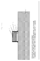
- Figure 12 illustrates different aspects of a method of the invention:
- the present invention provides a method for forming a gate stack in a MOSFET device, comprising the steps of:
- the present invention is based on the surprising discovery that the best results in terms of EOT reduction (Equivalent Oxide Thickness reduction) and eWF shift (effective work function shift) are obtained when the anneal (for said RES formation) step takes place only after the metal gate electrode has been deposited on said REO.
- the present invention is further based on the surprising discovery that there is an optimum ratio REO/(REO +SiCDM) for which the EOT is the lowest (see fig. 9 ). Indeed, a second unexpected observation was the increase of the EOT when departing away from that optimum REO/(REO +Si-CDM) ratio.
- Fig. 9 shows the effect of Dy 2 O 3 thickness on the EOT of SiON/Dy 2 O 3 stacks with a fixed SiON thickness (2 nm).
- the experiment result shows that the EOT actually decreases from 1.8 nm to 1.4 nm (18 to 14 ⁇ ) when the SiON is capped with 0.5- and 1-nm Dy 2 O 3 .
- the optimal Dy 2 O 3 /(Dy 2 O 3 +SiO 2 ) thickness ratio for minimal EOT is comprised between 0.2 and 0.4.
- Fig. 10 shows the effect of Dy 2 O 3 /(Dy 2 O 3 +SiO 2 ) thickness ratio thickness on the EOT of SiON/Dy 2 O 3 stacks with a fixed total Dy 2 O 3 +SiO 2 thickness (3 nm).
- the EOT of the SiO 2 /Dy 2 O 3 stack is a function of the Dy 2 O 3 /(Dy 2 O 3 +SiO 2 ) thickness ratio.
- the smallest EOT is obtained at a ratio comprised between about 0.3 and about 0.4, corresponding to an EOT reduction of 0.5 nm (5 ⁇ ) as compared to the uncapped SiO 2 .
- the effective work function (eWF) is inversely proportional to the ratio.
- the eWF decreases from 4.4 to 3.7 eV as the Dy 2 O 3 /(Dy 2 O 3 +SiO 2 ) thickness ratio increases from 0 to 0.7, and stabilizes at 3.7 eV with a ratio higher than 0.7.
- the optimal Dy 2 O 3 / (Dy 2 O 3 +SiO 2 ) thickness ratio is about 0.3 where the EOT reduction is maximized and the eWF is comparable to that of the SiON/poly reference (4.0 eV).
- Fig. 10 also shows that when nitrogen is added in SiO 2 , the EOT and eWF decrease by 0.2 nm (2 ⁇ ) and 150 mV, respectively, as compared to the SiO 2 /Dy 2 O 3 stack at the same the Dy 2 O 3 /(Dy 2 O 3 +SiO 2 ) thickness ratio.
- the EOT decrease may result from an increased dielectric constant or enhanced Dy 2 O 3 -SiO(N) intermixing due to the nitrogen incorporation.
- the eWF decrease may result from the positive charges induced by the nitrogen incorporation which was also seen on the HfSiO(N)/Ta 2 C stack.
- Fig. 11 shows the EOT and the eWF of Dy 2 O 3 -capped SiON from various thermal budgets and annealing sequences.
- S/D RTA standard activation anneal
- PDA post-deposition anneal
- a method of the invention for forming a gate stack in a MOSFET device comprises the steps of:
- said annealing step is performed at a temperature preferably comprised between 600°C and 1200°C, more preferably comprised between 600°C and 1000°C.
- said REO and said SiO 2 are provided in a ratio REO: (REO + SiO 2 ) comprised between 0.1 and 0.4, more preferably between 0.2 and 0.4, and even more preferably between 0.2 and 0.3.
- Said REO layer can be formed or deposited by MOCVD, ALD, AVD or PVD deposition technique.
- Said SiO 2 or SiON layer can be formed or deposited by MOCVD, ALD, AVD or PVD deposition technique.
- Said SiO 2 or SiON layer can further comprise Sc, Hf or Al.
- said REO layer can further comprise Sc, Hf or Al.
- both REO layer and SiO 2 (or SiON) layer can further comprise Sc, Hf or Al.
- said metal gate electrode can comprise (or consist of) W, Ta, Ti, Ru, Pt and/or Mo, more particularly can comprise (or consist of) TiN, TaN and/or Ru.
- said substrate can comprise (or consist of) a Ge, SiGe, GaAs, and/or InP layer.
- Said annealing step can be a post-deposition anneal or a RTA step.
- An object of the present invention is also a semiconductor device, more particularly a MOSFET device obtainable by a preferred method of the invention.
- a preferred MOSFET device of the invention comprises:
- Said RES layer results from the annealing of the SiO 2 or SiON layer and the REO layer (comprising Dy and/or La) that are deposited (or formed) upon said substrate, said annealing being performed only after having deposited said metal gate electrode.
- Said SiO 2 or SiON layer can further comprise Sc, Hf or Al.
- said RES layer can further comprise Sc, Hf or Al.
- both RES layer and SiO 2 (or SiON) layer can further comprise Sc, Hf or Al.
- Said metal gate electrode can comprise (or consist of) W, Ti, Ta, Pt, Ru and/or Mo, preferably can comprise (or consist of) TiN, TaN and/or Ru.
- Said substrate can comprise (or consist of) a Ge, SiGe, GaAs, and/or InP layer.
- Figure 1 (a) shows the physical thickness variation of the as deposited gate dielectrics upon anneal at different temperatures. On the X-axis are the ellipsometrically measured film thicknesses for the various gate dielectrics.
- Various deposition techniques like Atomic layer Deposition (ALD) and Atomic Vapor Deposition (AVD) have been employed.
- the films have been deposited on an interfacial SiO 2x silicon oxide like interface, which is not distinguishable from the ellipsometer result.
- the deposited bi-layer film stack has been annealed at temperatures approximately between 600°C and 1000°C in O 2 , the later to explicitly stimulate the film thickness increase.
- the bar graph for IMEC-clean indicates the silicon substrate oxidation as function of anneal treatment studied (reference).
- the IMEC-clean is a wet cleaning sequence comprising the steps of organic removal with SOM (Sulphuric acid- Ozone mixture), followed by APM (ammonium peroxide) cleaning and diluted HF/HC1 with DI (deionized) water rinses in between and Marangoni drying at the end. This substrate only received a clean thereby forming a chemical oxide.
- the thickness increase/layer reaction is thermally activated, the larger the thermal budget the larger the physical thickness, and fully deploying at temperatures of approximately 1000°C or above.
- the degree of reactivity i.e. the dependency of physical thickness on thermal budget, clearly depends on the species involved, with Dy (and La, see Fig 1(b) ) reacting more substantial than Sc (or even Si) containing films.
- the reactivity of the Dy containing films can be modulated with Sc addition.
- Figure 1 (b) shows the thickness variation of the as deposited ALD La 2 O 3 upon different anneal steps approximately from 600°C to 1000°C. Similar as for Dy, also for La a clear reactivity and hence physical thickness increase can be observed upon thermal annealing. However, as can be seen from Figure 1 (b) , La 2 O 3 shows a different behavior compared to Dy:
- the (rare earth) element used is one of the parameters that assist in controlling the dielectric properties of the final gate dielectric layer outcome at the end of the process.
- silicate formation When annealing a rare earth oxide (REO) layer or stack of layers deposited on top of silicon oxide , silicate formation can be witnessed for example as:
- REO rare earth oxide
- Figure 2 shows the normalized thickness increase (t annealed - t dep )/t dep for DyScO x layers annealed in O 2 (•: circle) or N 2 (A: triangle), where t annealed is the layer thickness after a thermal anneal at about 1000°C and t dep is the as-deposited thickness of the layer.
- the silicate formation is function of the thermal budget applied, i.e. depends on time as well as temperature, as shown in Figure 3 .
- Figure 3 shows the normalized thickness increase for an about 10 nm DyScO x layer after different thermal treatments (temperature and time).
- Figure 4 shows the normalized thickness increase (t annealed - t dep )/t dep (•: circle) and absolute thickness increase (A: triangle) after 1000°C anneal for a DyScOx layer as function of the as-deposited thickness.
- Figure 5 shows the normalized thickness increase (t annealed - t dep )/t dep after a 1000°C anneal for DyScOx layers as function of the anneal time: Dy-rich (about 75%Dy) (•: circle); Sc-rich (about 25%Dy) ( ⁇ : square).
- Figure 6 shows the relative thickness increase (%) as function of the Dy concentration (%) for two different compounds: DyHfOx ( ⁇ : square) and DyScOx (•: circle).
- DyScO x layers rather behave as Dy 2 O 3 layers (extensive silicate formation) except for the more Sc-rich layers, incorporation of Hf is clearly seen to limit the silicate formation (less thickness increase since less SiO 2 incorporation) up to the very Dy-rich DyHfOx layers.
- silicate formation can only occur by mixing of the RE oxide with the SiO 2 present in the underlying layer. This mixing results in a drop of the density of the RE oxide. This density drop is proportional to the ratio of RE/SiO 2 .
- the ideal metal gate needs a tunable work function with process conditions "similar" to classical silicon technologies. This implicitly suggests gaining control of the interface polarization between the metal and the dielectric to engineer the gate work function.
- Results indicate that Al can be used to shift the threshold voltage upwards (of interest for PMOS), as opposed to rare earth elements that were found to shift the threshold voltage to lower values (of interest for NMOS).
- Dy-based oxides show unexpectedly good results when implemented as cap layers.
- Figure 7 presents the threshold voltage shift for Dy-based and Sc-based oxides and a combination thereof.
- the magnitude of the effect is the result of a complex equation with for example the composition of the gate dielectric and metal gate as input parameters.
- the SiO 2 thickness can be controlled through thermal oxidation of the substrate prior to any high-k deposition.
- the various nanometer thick high-k dielectric films can be deposited by a range of techniques - preferably chemical vapor deposition like, either as nanolaminates or as co-deposited films.
- the composition of the film can be controlled.
- the thickness of SiO 2 and composition/thickness of the high-k films ought to be selected such that after application of a thermal budget, a suitable EOT is obtained.
- a SiON dielectric film of thickness 2nm has been capped by 1nm of Dy 2 O 3 and capped with a TaN metal electrode as shown in Figure 8 (a) .
- a junction activation thermal budget (1030°C)
- a gate stack EOT has been extracted, clearly less than the original 2nm SiON.
- a reduction in EOT from ⁇ 1.8nm down to 1.3nm EOT has been observed, as well as a reduction in Vt as shown in Figure 8 (b) .
- a similar experiment has been done using HfSiON dielectrics with Dy 2 O 3 cap.
Abstract
Description
- The present invention relates to semiconductor process technology and devices.
- In particular, the present invention relates to a method for forming a gate stack in a MOSFET device and the MOSFET device obtainable by said method.
- Ono et al. (Appl. Phys. Lett., 78, 1832 (2001)) have described that the rare earth (RE) elements, for example lanthanum, in contact with SiO2 in an oxygen containing ambient react to form a silicate when heated to sufficiently high temperatures.
- Depending on the nature of the element, the intensity of the silicate formation will vary. As a result of this, silicate formation may have different consequences.
- One consequence is the consumption of the interface region between the rare earth element and the silicon-oxide resulting in a reduction of the equivalent oxide thickness (EOT) as observed by Lichtenwahlner et al. (J. Appl. Phys., 98, 024314 (2005)).
- Another consequence is the shift of the threshold voltage towards lower values as reported by L. Pantisano et al. (Appl. Phys. Lett., 89, 113505 (2006)), when these rare earth materials are integrated in the gate stack as a cap layer of monolayer(s) thickness.
- The present invention relates to a method for forming a gate stack in a MOSFET device, comprising the steps of:
- forming, on a semiconductor substrate, at least one layer of a dielectric material, the upper layer comprising (or consisting of) a Si containing dielectric material (Si-CDM),
- depositing (immediately) on said Si-CDM, at least one rare earth oxide (REO) layer,
- depositing (immediately) on said REO layer, at least one layer of a suitable material for forming a metal gate electrode, and
- after having deposited said material suitable for forming a metal gate electrode on said REO layer, annealing (for obtaining a reaction, at least partially, between said Si-CDM and said REO layer), whereby a rare earth silicate (RES) layer is formed,
- In a method according to the invention, no annealing step is performed before the deposition of said metal gate.
- Preferably, said annealing step is performed immediately after said metal gate deposition.
- Preferably, said annealing step is a PDA step (post-deposition annealing step).
- Said annealing step can be a RTA step (Rapid Thermal Anneal step).
- Preferably (and alternatively), said annealing step can be performed after spacer definition. A method of the invention can further comprise, before the annealing step, the steps of polySi deposition, gate patterning and spacers formation.
- Said annealing step can be a source/drain RTA step after spacer definition.
- Said annealing step can comprise a source/drain RTA step and a PDA step, after spacer definition.
- In a method according to the invention, said annealing step is preferably performed at a temperature higher than (about) 600°C, preferably comprised between (about) 600°C and (about) 1200°C, more preferably comprised between (about) 600°C and (about) 1000°C.
- More preferably, said annealing step is performed at a temperature higher than (about) 800°C, preferably comprised between (about) 800°C and (about) 1200°C, more preferably comprised between (about) 800°C and (about) 1000°C.
- Preferably, said REO and said Si-CDM are provided in a ratio REO:(REO + Si(CDM)) comprised between (about) 0.05 and (about) 0.4, more preferably between (about) 0.1 and (about) 0.4, even more preferably between (about) 0.2 and (about) 0.35, and even more preferably between (about) 0.2 and (about) 0.3.
- In a method of the invention said at least one layer of a dielectric material preferably consists of said Si-CDM. In other words, preferably, in a method of the invention, at least one layer comprising (or consisting of) a Si-CDM is formed on said semiconductor substrate.
- Said Si-CDM layer can comprise (or consist of) any suitable high-k material (i.e. any suitable material the dielectric constant of which is higher than the dielectric constant of SiO2; i.e. k > kSiO2).
- Preferably, said at least one layer of Si-CDM comprises (or consists of) SiO2.
- In a method according to the invention, said at least one layer of Si-CDM can comprise or further comprise nitrogen. More particularly, said at least one layer of Si-CDM comprises (or consists of) SiON.
- Preferably, said Si-CDM is formed or deposited by MOCVD, ALD, AVD or PVD deposition technique.
- In a method of the invention said at least one layer of REO can comprise (or consist of) any of La, Y, Pr, Nd, Sm, Eu, Gd, Dy, Er, or Yb, or any combination of 2, 3 or more thereof. More particularly, said at least one layer of REO can comprise (or consist of) any of La-, Y-, Pr-, Nd-, Sm-, Eu-, Gd-, Dy-, Er-, or Yb-based oxides, or any combination of 2, 3 or more thereof.
- Preferably, in a method of the invention said at least one layer of REO can comprise (or consist of) La and/or Dy based oxides.
- More preferably, said REO layer comprises (or consists of) dysprosium oxide.
- Preferably, said at least one REO layer is deposited by MOCVD, ALD, AVD or PVD deposition technique.
- In a method of the invention said at least one layer of REO can result from the oxidation of a layer rare earth element.
- In a method of the invention said at least one layer of Si-CDM and/or said at least one layer of REO can further comprise a modulator element, such as Al, Hf, or Sc.
- Said modulator can be added to said REO layer for increasing the thermal stability of the layer.
- In particular, said modulator element can be added to said Si-CDM layer and/or to said REO layer for enhancing or reducing the RES formation. More particularly, Hf and Sc hinder the RES formation; whereas Al is an enhancer of said RES formation.
- Preferably, said REO layer comprises (or consists of) dysprosium scandate.
- Preferably, said modulator is added to said REO layer in a ratio Modulator: (Modulator + RE) of about 50%.
- Said modulator can be an enhancer element (such as Al), whereby the intermixing is enhanced. For example, Al can be added to the REO in a ratio Al:(Al+RE) smaller than (about) 75%.
- Preferably, in a method according to the invention, said metal gate electrode comprises (or consists of) W, Ta, Ti, Ru, Pt and/or Mo, preferably TiN, TaN and/or Ru.
- Preferably, in a method according to the invention, said substrate comprises (or consists of) a Ge, SiGe, GaAs, and/or InP layer.
- The invention relates also to a method for reducing the EOT of a gate stack in a MOSFET device, by capping a Si containing dielectric layer with a REO and annealing (forming a RES layer) after depositing a metal gate electrode.
- Said method for reducing the EOT of a gate stack in a MOSFET device can comprise the same steps as a method of the invention for forming a gate stack in a MOSFET device.
- In particular, the EOT can be reduced of at least 0.1 nm EOT when the ratio REO: (REO + Si(CDM)) is comprised between (about) 0.05 and (about) 0.4, more particularly between (about) 0.1 and (about) 0.4, even more particularly between (about) 0.2 and (about) 0.35, and even more particularly between (about) 0.2 and (about) 0.3.
- Alternatively, in a second embodiment, instead of the REO formation, a method of the invention can be carried out with the deposition of a layer of a rare earth element (RE element), the oxidation of which being prevented. More particularly, the RE layer can be deposited in-situ, i.e. with no vacuum break between said RE deposition and the metal gate deposition.
- In that embodiment, the RES results from the annealing of said Si-CDM layer and said RE layer.
- More particularly, a method for forming a gate stack in a MOSFET device, according to said second embodiment can comprise the steps of:
- forming, on a semiconductor substrate, at least one layer of a dielectric material, the upper layer comprising a Si containing dielectric material (Si-CDM), preferably SiO2 or SiON,
- depositing on said Si-CDM, at least one rare earth (RE) layer,
- depositing on said RE layer, at least one layer of a suitable material for forming a metal gate electrode, and
- after having deposited said material suitable for forming a metal gate electrode on said RE layer, annealing (for obtaining a reaction, at least partially, between said Si-CDM and said RE layer), whereby a rare earth silicate (RES) layer is formed,
- The other conditions and parameters used herein also apply to that embodiment.
- The method of the invention can also be carried out for forming capacitors such as metal-insulator-metal capacitors wherein the dielectric stack constitutes the dielectric part of such capacitor.
- More particularly, a method of the invention for forming capacitors, such as metal-insulator-metal capacitors, comprises the steps of:
- forming, on a material suitable for forming an electrode, at least one layer comprising (or consisting of) a Si-CDM,
- depositing (immediately) on said Si-CDM, at least one REO or RE layer,
- depositing (immediately) on said REO or RE layer, at least one layer of a material suitable for forming an electrode, and
- after having deposited said material suitable for forming an electrode on said REO or RE layer, annealing (for obtaining a reaction, at least partially, between said Si-CDM and said REO or RE layer), whereby a rare earth silicate (RES) layer is formed,
- Another object of the present invention is a semiconductor device obtainable by a method according to the invention.
- In particular, the present invention also relates to a capacitor, such as metal-insulator-metal capacitor.
- And more particularly, the present invention also relates to a MOSFET device obtainable by a method according to the invention.
- In particular, a MOSFET device according to the invention comprises:
- a semiconductor substrate,
- a gate dielectric comprising (or consisting of) at least one layer of a dielectric material, the upper layer comprising (or consisting of) a Si-CDM,
- upon said Si-CDM, a RES layer, and
- upon said RES layer, a metal gate electrode,
- A MOSFET device according to the invention can further comprise unreacted REO or unreacted RE. A REO or RE layer can remain between said RES and said metal gate electrode.
- A MOSFET device according to the invention can further comprise a polySi layer on said metal gate electrode.
- Preferably, said at least one layer of dielectric material consists of said Si-CDM.
- Preferably, said at least one layer of Si-CDM comprises SiO2, SiON, HfSiO, or HfSiON.
- More preferably, said at least one layer of Si-CDM consists of SiO2, SiON, HfSiO, or HfSiON.
- Preferably, said REO or RE layer comprises (or consists of) any of La, Y, Pr, Nd, Sm, Eu, Gd, Dy, Er, Yb or any combination of 2, 3 or more thereof.
- More preferably, said REO layer comprises (or consists of) any of La-, Y-, Pr-, Nd-, Sm-, Eu-, Gd-, Dy-, Er-, and Yb- based oxides or any combination of 2, 3 or more thereof. Even more preferably, said REO layer comprises (or consists of) any of La and/or Dy based oxides, and more particularly dysprosium oxide, or dysprosium scandate.
- Preferably, said metal gate electrode comprises (or consists of) W, Ti, Ta, Pt, Ru and/or Mo, preferably TiN, TaN and/or Ru.
- Preferably, said substrate comprises (or consists of) a Ge, SiGe, GaAs, and/or InP layer.
-
Figure 1 (a) shows the physical thickness variation of the as deposited gate dielectrics upon anneal at different temperatures. -
Figure 1 (b) shows the thickness variation of the as depositedALD La 203 upon different anneal steps approximately from 600°C to 1000°C. -
Figure 2 shows the normalized thickness increase (tannealed - tdep)/tdep for DyScOx layers annealed in O2 (•: circle) or N2 (A: triangle), where tannealed is the layer thickness after a thermal anneal at about 1000°C and tdep is the as-deposited thickness of the layer. -
Figure 3 shows the normalized thickness increase for an about 10 nm DyScOx layer after different thermal treatments (temperature and time). -
Figure 4 . shows the normalized thickness increase (tannealed - tdep)/tdep (•: circle) and absolute thickness increase (A: triangle) after 1000°C anneal for a DyScOx layer as function of the as-deposited thickness. -
Figure 5 shows the normalized thickness increase (tannealed - tdep)/tdep after a 1000°C anneal for DyScOx layers as function of the anneal time: Dy-rich (about 75%Dy) (•: circle); Sc-rich (about 25%Dy) (■: square) . -
Figure 6 shows the relative thickness increase (%) as function of the Dy concentration (%) for two different compounds: DyHfOx (■: square) and DyScOx (•: circle). -
Figure 7 presents the threshold voltage (Vt) shift for Dy-based and Sc-based oxides and a combination thereof. - In
Figure 8 (a) , as a demonstration, a SiON dielectric film of 2 nm thickness has been capped by 1 nm of Dy2O3 and capped with a TaN metal electrode. After application of a junction activation thermal budget (1030°C), a gate stack EOT has been extracted, clearly less than the original 2 nm SiON. A reduction in EOT from about 1.8 nm down to 1.3 nm EOT has been observed, as well as a reduction in Vt as shown inFigure 8 (b) . -
Figure 9 shows the effects of Dy2O3 cap thicknesses on the EOT of SiON/Dy2O3/TaN. -
Figure 10 shows the EOT and eWF of SiO(N)/Dy2O3/TaN as a function of Dy2O3/ (Dy2O3+SiO (N)) thickness ratio. -
Figure 11 shows hte EOT and eWF of SiO(N)/Dy2O3/TaN with various thermal budgets and annealing sequences. -
Figure 12 illustrates different aspects of a method of the invention: - (a) before a PDA annealing, the stack of layers comprises the substrate (1), the Si-CDM (2, 2a), the REO (4) and the metal gate (5);
- (b) after the PDA annealing of the stack of layers as illustrated in (a), the resulting stack of layers comprises the substrate (1), the Si-CDM (2a), the RES (3), possibly remaining REO (4a), and the metal gate (5);
- (c) before the annealing step, the stack of layers comprises the substrate (1), the Si-CDM (2, 2a), the REO (4), the metal gate (5), the polySi (6) and the spacers (7); and
- (d) after said annealing step (performed after spacers definition), the resulting stack of layers comprises the substrate (1), the Si-CDM (2a), the RES (3), possibly remaining REO (4a), the metal gate (5), the polySi (6) and the spacers (7).
- The present invention provides a method for forming a gate stack in a MOSFET device, comprising the steps of:
- forming, on a semiconductor substrate, at least one layer of a dielectric material (2, 2a), the upper layer comprising (or consisting of) a Si-CDM,
- depositing (preferably immediately) on said Si-CDM, at least one rare earth oxide (REO) layer (4),
- depositing (preferably immediately) on said REO layer (4), at least one layer of a suitable material for forming a metal gate electrode (5), and
- after having deposited said material suitable for forming a metal gate electrode on said REO layer, annealing (for obtaining a reaction, at least partially, between said Si-CDM and said REO layer), whereby a rare earth silicate (RES) layer is formed,
- The present invention is based on the surprising discovery that the best results in terms of EOT reduction (Equivalent Oxide Thickness reduction) and eWF shift (effective work function shift) are obtained when the anneal (for said RES formation) step takes place only after the metal gate electrode has been deposited on said REO.
- The present invention is further based on the surprising discovery that there is an optimum ratio REO/(REO +SiCDM) for which the EOT is the lowest (see
fig. 9 ). Indeed, a second unexpected observation was the increase of the EOT when departing away from that optimum REO/(REO +Si-CDM) ratio. -
Fig. 9 shows the effect of Dy2O3 thickness on the EOT of SiON/Dy2O3 stacks with a fixed SiON thickness (2 nm). - If assuming Dy2O3 and SiON do not intermix, the calculated EOT (open circles) increases with the Dy2O3 cap thickness.
- However, the experiment result shows that the EOT actually decreases from 1.8 nm to 1.4 nm (18 to 14 Å) when the SiON is capped with 0.5- and 1-nm Dy2O3.
- However, when the Dy2O3 thickness increases to 2 nm, the EOT increases again, agreeing with the calculated value assuming no mixing.
- This indicates that the intermixing between Dy2O3 and SiON only occurs at certain Dy2O3/(Dy2O3+SiO2) thickness ratio. The optimal Dy2O3/(Dy2O3+SiO2) thickness ratio for minimal EOT is comprised between 0.2 and 0.4.
-
Fig. 10 shows the effect of Dy2O3/(Dy2O3+SiO2) thickness ratio thickness on the EOT of SiON/Dy2O3 stacks with a fixed total Dy2O3+SiO2 thickness (3 nm). - The EOT of the SiO2/Dy2O3 stack is a function of the Dy2O3/(Dy2O3+SiO2) thickness ratio.
- The smallest EOT is obtained at a ratio comprised between about 0.3 and about 0.4, corresponding to an EOT reduction of 0.5 nm (5 Å) as compared to the uncapped SiO2.
- However, with the Dy2O3/(Dy2O3+SiO2) thickness ratios of 0.6 and above, the EOT increases and exceeds that of the uncapped SiO2.
- Unlike EOT, which exhibits a parabolic relationship with the Dy2O3/(Dy2O3+SiO2) thickness ratio, the effective work function (eWF) is inversely proportional to the ratio.
- The eWF decreases from 4.4 to 3.7 eV as the Dy2O3/(Dy2O3+SiO2) thickness ratio increases from 0 to 0.7, and stabilizes at 3.7 eV with a ratio higher than 0.7.
- The optimal Dy2O3/ (Dy2O3+SiO2) thickness ratio is about 0.3 where the EOT reduction is maximized and the eWF is comparable to that of the SiON/poly reference (4.0 eV).
-
Fig. 10 also shows that when nitrogen is added in SiO2, the EOT and eWF decrease by 0.2 nm (2 Å) and 150 mV, respectively, as compared to the SiO2/Dy2O3 stack at the same the Dy2O3/(Dy2O3+SiO2) thickness ratio. The EOT decrease may result from an increased dielectric constant or enhanced Dy2O3-SiO(N) intermixing due to the nitrogen incorporation. - The eWF decrease may result from the positive charges induced by the nitrogen incorporation which was also seen on the HfSiO(N)/Ta2C stack.
-
Fig. 11 shows the EOT and the eWF of Dy2O3-capped SiON from various thermal budgets and annealing sequences. - Besides the standard activation anneal ("S/D RTA") at 1030°C, an additional post-deposition anneal (PDA) at 1050°C was performed either after the S/D RTA ("S/D RTAS + PDA") or before the metal gate deposition ("PDA before TaN + S/D RTA").
- By comparing "S/D RTA only" and "S/D RTAS + PDA," it can be shown that an additional PDA increases the eWF only slightly, rendering the eWF shift (ΔeWF2) slightly smaller.
- However, when the PDA is performed on the as-deposited Dy2O3 before metal gate deposition ("PDA before TaN + S/D RTA"), the eWF shift (ΔeWF3) decreases substantially by 220 meV.
- This shows that to achieve the maximal eWF tuning, the (high-temperature) anneal needs to be performed after the Dy2O3 cap is covered/enclosed, in this example, by the metal gate, poly electrode, and spacer.
- According to a preferred embodiment, a method of the invention for forming a gate stack in a MOSFET device, comprises the steps of:
- forming, on a semiconductor substrate, one layer of SiO2 or one layer of SiON,
- forming or depositing on said SiO2 or said SiON, one dysprosium scandate layer, or one lanthanum oxide layer, or preferably one dysprosium oxide layer,
- depositing on the REO layer, at least one layer of a suitable material for forming a metal gate electrode, preferably a TaN layer, and
- after having deposited said material suitable for forming a metal gate electrode on said REO layer, annealing (for obtaining a reaction, at least partial, between said SiO2 or SiON layer and said REO layer, whereby a rare earth silicate (RES) layer is formed,
- Depending on the substrate, said annealing step is performed at a temperature preferably comprised between 600°C and 1200°C, more preferably comprised between 600°C and 1000°C.
- Preferably, said REO and said SiO2 (or said SiON) are provided in a ratio REO: (REO + SiO2) comprised between 0.1 and 0.4, more preferably between 0.2 and 0.4, and even more preferably between 0.2 and 0.3.
- Said REO layer can be formed or deposited by MOCVD, ALD, AVD or PVD deposition technique.
- Said SiO2 or SiON layer can be formed or deposited by MOCVD, ALD, AVD or PVD deposition technique.
- Said SiO2 or SiON layer can further comprise Sc, Hf or Al.
- Alternatively, said REO layer can further comprise Sc, Hf or Al.
- Possibly, both REO layer and SiO2 (or SiON) layer can further comprise Sc, Hf or Al.
- In a preferred method of the invention, said metal gate electrode can comprise (or consist of) W, Ta, Ti, Ru, Pt and/or Mo, more particularly can comprise (or consist of) TiN, TaN and/or Ru.
- In a preferred method of the invention, said substrate can comprise (or consist of) a Ge, SiGe, GaAs, and/or InP layer.
- Said annealing step can be a post-deposition anneal or a RTA step.
- An object of the present invention is also a semiconductor device, more particularly a MOSFET device obtainable by a preferred method of the invention.
- In particular, a preferred MOSFET device of the invention comprises:
- a semiconductor substrate,
- a gate dielectric comprising a SiO2 or a SiON layer,
- upon and contacting said SiO2 or SiON layer, a rare earth silicate (RES) layer comprising Dy and/or La, and
- a metal gate electrode.
- Said RES layer results from the annealing of the SiO2 or SiON layer and the REO layer (comprising Dy and/or La) that are deposited (or formed) upon said substrate, said annealing being performed only after having deposited said metal gate electrode.
- Said SiO2 or SiON layer can further comprise Sc, Hf or Al.
- Alternatively, said RES layer can further comprise Sc, Hf or Al.
- Possibly, both RES layer and SiO2 (or SiON) layer can further comprise Sc, Hf or Al.
- Said metal gate electrode can comprise (or consist of) W, Ti, Ta, Pt, Ru and/or Mo, preferably can comprise (or consist of) TiN, TaN and/or Ru.
- Said substrate can comprise (or consist of) a Ge, SiGe, GaAs, and/or InP layer.
-
Figure 1 (a) shows the physical thickness variation of the as deposited gate dielectrics upon anneal at different temperatures. On the X-axis are the ellipsometrically measured film thicknesses for the various gate dielectrics. Various deposition techniques like Atomic layer Deposition (ALD) and Atomic Vapor Deposition (AVD) have been employed. - The films have been deposited on an interfacial SiO2x silicon oxide like interface, which is not distinguishable from the ellipsometer result.
- The deposited bi-layer film stack has been annealed at temperatures approximately between 600°C and 1000°C in O2, the later to explicitly stimulate the film thickness increase.
- The bar graph for IMEC-clean indicates the silicon substrate oxidation as function of anneal treatment studied (reference). The IMEC-clean is a wet cleaning sequence comprising the steps of organic removal with SOM (Sulphuric acid- Ozone mixture), followed by APM (ammonium peroxide) cleaning and diluted HF/HC1 with DI (deionized) water rinses in between and Marangoni drying at the end. This substrate only received a clean thereby forming a chemical oxide.
- It can be seen that the thickness increase/layer reaction is thermally activated, the larger the thermal budget the larger the physical thickness, and fully deploying at temperatures of approximately 1000°C or above. However, the degree of reactivity, i.e. the dependency of physical thickness on thermal budget, clearly depends on the species involved, with Dy (and La, see
Fig 1(b) ) reacting more substantial than Sc (or even Si) containing films. Moreover, the reactivity of the Dy containing films can be modulated with Sc addition. -
Figure 1 (b) shows the thickness variation of the as deposited ALD La2O3 upon different anneal steps approximately from 600°C to 1000°C. Similar as for Dy, also for La a clear reactivity and hence physical thickness increase can be observed upon thermal annealing. However, as can be seen fromFigure 1 (b) , La2O3 shows a different behavior compared to Dy: - a reactivity at lower temperatures (about 800°C),
- moreover, the thickness increase does not depend on the as deposited thickness of the La2O3 layers.
- This shows that the (rare earth) element used is one of the parameters that assist in controlling the dielectric properties of the final gate dielectric layer outcome at the end of the process.
- When annealing a rare earth oxide (REO) layer or stack of layers deposited on top of silicon oxide , silicate formation can be witnessed for example as:
- a) in the absence of an additional oxygen supply: a density decrease of the rare earth (RE) oxide layer because of intermixing of the RE oxide with silicon oxide , but without any significant thickness change of the total dielectric stack, as shown in
Figure 2 (N2 atmosphere); - b) in the presence of an oxygen source: as a thickness increase caused by a volume expansion due to the incorporation of Si or SiO2, at the reaction front between rare earth film and the silicon oxide film in addition to the regrown or the already present SiO2 before deposition as shown in
Figure 2 (O2 atmosphere). -
Figure 2 shows the normalized thickness increase (tannealed - tdep)/tdep for DyScOx layers annealed in O2 (•: circle) or N2 (A: triangle), where tannealed is the layer thickness after a thermal anneal at about 1000°C and tdep is the as-deposited thickness of the layer. - Besides the ambient used during the anneal step, the silicate formation is function of the thermal budget applied, i.e. depends on time as well as temperature, as shown in
Figure 3 . -
Figure 3 shows the normalized thickness increase for an about 10 nm DyScOx layer after different thermal treatments (temperature and time). - For the example of DyScOx, it is clear that the thickness increases more as temperature goes up, especially at temperatures exceeding about 900°C. It can also be seen that the initial silicate formation occurs very fast before stabilizing to an equilibrium value that can be interpreted as the maximum solubility of SiO2 in DyScOx.
-
Figure 4 . shows the normalized thickness increase (tannealed - tdep)/tdep (•: circle) and absolute thickness increase (A: triangle) after 1000°C anneal for a DyScOx layer as function of the as-deposited thickness. -
Figure 5 shows the normalized thickness increase (tannealed - tdep)/tdep after a 1000°C anneal for DyScOx layers as function of the anneal time: Dy-rich (about 75%Dy) (•: circle); Sc-rich (about 25%Dy) (■: square). - The maximum amount of SiO2 that can be incorporated in the gate dielectric film stack will depend on the amount of rare earth material present (see also
Figure 1 (a) ). This is evidenced by: - a) the relation between the relative thickness increase and the thickness of the as-deposited rare earth oxide, i.e. the thicker the as-deposited layer, the more SiO2 can be incorporated as shown in
Figure 4 . When considering the relative thickness increase it is clear that the system strives to a certain equilibrium composition, based on the graph below. This equilibrium composition is approximately about 2:1 RE:SiO2. This ratio is determined by the composition of the rare earth layer (see belowFigure 4 for DyScOx) and not by the physical thickness of the layer. - b) the different behavior of ~10-nm thick DyScOx layers with different composition. The relative thickness increase clearly depends on the composition of the DyScOx layer, where the Dy-rich layer, i.e. the layer that contains the most amount of Dy demonstrates a much larger thickness increase as compared to the Sc-rich layer as shown in
Figure 5 . This again demonstrates that the amount of SiO2 that can be incorporated in the stack depends on the amount of Dy present. - The behavior described above corresponds to an unlimited supply of oxygen, i.e. where all anneal treatments in a process flow for manufacturing a semiconductor device comprising a gate stack according to the present invention are done in an oxygen ambient. In that case the system will evolve to a condition where the maximum amount of SiO2 can be incorporated.
- An influence is also seen from the element that is incorporated (co-deposited) in the gate dielectric stack.
-
Figure 6 shows the relative thickness increase (%) as function of the Dy concentration (%) for two different compounds: DyHfOx (■: square) and DyScOx (•: circle). - Comparing for example DyScOx with DyHfOx layers with varying composition, it is clear that both stacks behave differently as shown in
Figure 6 . - Whereas DyScOx layers rather behave as Dy2O3 layers (extensive silicate formation) except for the more Sc-rich layers, incorporation of Hf is clearly seen to limit the silicate formation (less thickness increase since less SiO2 incorporation) up to the very Dy-rich DyHfOx layers.
- The behavior described above corresponds to an unlimited supply of oxygen.
- For the case where the anneal is performed without additional oxygen supply, e.g. anneal in N2 or for a layer covered (capped) with an oxygen impermeable layer, silicate formation can only occur by mixing of the RE oxide with the SiO2 present in the underlying layer. This mixing results in a drop of the density of the RE oxide. This density drop is proportional to the ratio of RE/SiO2. Once all SiO2 has been able to react, the system will reach a stable state. The state is stable as long as the system is closed, i.e. the gate dielectric is covered (capped) with a metal gate layer on top preventing exposure of the gate dielectric to oxygen and/or no further thermal budgets are applied in an oxygen-containing ambient with a magnitude above the threshold for a given gate dielectric layer formed.
- To achieve high performances, the ideal metal gate needs a tunable work function with process conditions "similar" to classical silicon technologies. This implicitly suggests gaining control of the interface polarization between the metal and the dielectric to engineer the gate work function.
- In that respect, the introduction of controlled chemical "impurities" at the dielectric/metal interface is a promising approach. The impact of a low concentration [about 1013 atm/cm2] of electropositive elements (such as Rb, Sr, Y, Cs, etc.) at the SiO2/TiN and HfO2/TiN interfaces has been modeled using a simple approach based on the derivation of the atomic partial charges present at the interface [Smith, J.Chem.Edu, vol 67, p 559, 1990] and on the potential they generate (within a punctual charge treatment). The models revealed that the work function of TiN could be shifted up to about 0.35 eV, depending on both the nature of the chemical elements and the oxide considered.
- Bringing this to practice means that - as a function of thermal budget applied - the interface region between gate electrode and gate dielectric (or gate dielectric stack) can be modified such that an appropriate work function is achieved. Experimental evidence has been gained for this observation through selective introduction of cap layers - i.e. an ultra-thin (sub nanometer) dielectric deposited in between host dielectric and gate electrode - or alternative dielectric stacks. The new dielectrics that have been explored for use as a bulk dielectric or cap layer are combinations of scandium, dysprosium, lanthanum, aluminum, and hafnium.
- Results indicate that Al can be used to shift the threshold voltage upwards (of interest for PMOS), as opposed to rare earth elements that were found to shift the threshold voltage to lower values (of interest for NMOS).
- Dy-based oxides show unexpectedly good results when implemented as cap layers.
Figure 7 presents the threshold voltage shift for Dy-based and Sc-based oxides and a combination thereof. The magnitude of the effect is the result of a complex equation with for example the composition of the gate dielectric and metal gate as input parameters. - Further an example is given on how the parameters can be controlled in order to obtain the targeted EOT and Vt.
- The SiO2 thickness can be controlled through thermal oxidation of the substrate prior to any high-k deposition.
- The various nanometer thick high-k dielectric films can be deposited by a range of techniques - preferably chemical vapor deposition like, either as nanolaminates or as co-deposited films. The composition of the film can be controlled. The thickness of SiO2 and composition/thickness of the high-k films ought to be selected such that after application of a thermal budget, a suitable EOT is obtained.
- As a demonstration, a SiON dielectric film of thickness 2nm has been capped by 1nm of Dy2O3 and capped with a TaN metal electrode as shown in
Figure 8 (a) . After application of a junction activation thermal budget (1030°C), a gate stack EOT has been extracted, clearly less than the original 2nm SiON. A reduction in EOT from ~1.8nm down to 1.3nm EOT has been observed, as well as a reduction in Vt as shown inFigure 8 (b) . Also, a similar experiment has been done using HfSiON dielectrics with Dy2O3 cap.
wherein there is no annealing step before having deposited said material suitable for forming a metal gate electrode on said RE layer.
Claims (35)
- A method for forming a gate stack in a MOSFET device, comprising the steps of:- forming, on a semiconductor substrate (1), at least one layer of a dielectric material (2, 2a), the upper layer comprising a Si containing dielectric material (Si-CDM),- depositing on said Si-CDM, at least one rare earth oxide (REO) layer (4),- depositing on said REO layer (4), at least one layer of a suitable material for forming a metal gate electrode (5), and- after having deposited said material suitable for forming a metal gate electrode on said REO layer, annealing, whereby a rare earth silicate (RES) layer is formed,wherein there is no annealing step before having deposited said material suitable for forming a metal gate electrode on said REO layer.
- A method according to claim 1, wherein said REO and said Si-CDM are provided in a ratio REO: (REO + Si(CDM)) comprised between 0.1 and 0.4.
- A method according to claim 1, wherein said REO and said Si-CDM are provided in a ratio REO: (REO + Si(CDM)) comprised between 0.2 and 0.3.
- A method according to any of claims 1 to 3, wherein said at least one REO layer is formed or deposited by MOCVD, ALD, AVD or PVD deposition technique.
- A method according to any of claims 1 to 4, wherein said REO layer (4) comprises any of La, Y, Pr, Nd, Sm, Eu, Gd, Dy, Er, or Yb, or any combination of 2, 3 or more thereof, more particularly any of La, Y, Pr, Nd, Sm, Eu, Gd, Dy, Er, or Yb based oxides, or any combination of 2, 3 or more thereof.
- A method according to claim 5, wherein said REO layer (4) comprises any of La and/or Dy based oxides.
- A method according to any of claims 1 to 6, wherein said REO layer (4) comprises dysprosium oxide.
- A method according to any of claims 1 to 6, wherein said REO layer (4) comprises dysprosium scandate.
- A method according to any of claims 1 to 8, wherein said REO layer (4) further comprises Sc, Hf or Al.
- A method for forming a gate stack in a MOSFET device, comprising the steps of:- forming, on a semiconductor substrate, at least one layer of a dielectric material, the upper layer comprising a Si containing dielectric material (Si-CDM),- depositing on said Si-CDM, at least one rare earth (RE) layer,- depositing on said RE layer, at least one layer of a suitable material for forming a metal gate electrode, and- after having deposited said material suitable for forming a metal gate electrode on said RE layer, annealing, whereby a rare earth silicate (RES) layer is formed,wherein oxidation of said RE layer is prevented, and
wherein there is no annealing step before having deposited said material suitable for forming a metal gate electrode on said RE layer. - A method according to any of claims 1 to 10, wherein said layer of Si-CDM comprises any suitable high-k material (i.e. k > kSiO2).
- A method according to any of claims 1 to 11, wherein said layer of Si-CDM comprises SiO2.
- A method according to any of claims 1 to 11, wherein said layer of Si-CDM consists of SiO2.
- A method according to any of claims 1 to 13, wherein said layer of Si-CDM comprises or further comprises nitrogen.
- A method according to claim 14, wherein said layer of Si-CDM consists of SiON.
- A method according to any of claims 1 to 15, wherein said annealing step is performed at a temperature higher than 600°C, preferably comprised between 600°C and 1200°C, more preferably comprised between 600°C and 1000°C.
- A method according to any of claims 1 to 15, wherein said annealing step is performed at a temperature higher than 800°C, preferably comprised between 800°C and 1200°C, more preferably comprised between 800°C and 1000°C.
- A method according to any of claims 1 to 17, wherein said Si-CDM is formed or deposited by MOCVD, ALD, AVD or PVD deposition technique.
- A method according to any of claims 1 to 18, wherein said metal gate electrode (5) comprises W, Ta, TI, Ru, Pt and/or Mo, preferably TiN, TaN and/or Ru.
- A method according to any of claims 1 to 19, wherein said substrate (1) comprises a Ge, SiGe, GaAs, and/or InP layer.
- A method according to any of claims 1 to 20, wherein said annealing step is a post-deposition anneal.
- A method according to any of claims 1 to 20, wherein said annealing step is a Rapid Thermal Anneal.
- A MOSFET device obtainable by a method according to any of claims 1 to 22.
- A MOSFET device according to claim 23 comprising:- a semiconductor substrate (1),- a gate dielectric comprising at least one layer of a dielectric material, the upper layer comprising (or consisting of) a Si containing dielectric material (Si-CDM) (2a),- upon said Si-CDM (2a), a rare earth silicate (RES) layer (3), and- upon said RES layer (3), a metal gate electrode (5),wherein said RES layer (3) results from the annealing of said Si-CDM and said REO or RE layer, said annealing being performed only after having deposited said metal gate electrode.
- A MOSFET device according to claim 23 or 24, further comprising an unreacted REO layer (4a) or unreacted RE layer.
- A MOSFET device according to any of claims 23 to 25, further comprising a polySi layer (6) on said metal gate electrode (5).
- A MOSFET device according to any of claims 23 to 26, wherein said layer of Si-CDM comprises SiO2, SiON, HfSiO, or HfSiON.
- A MOSFET device according to any of claims 23 to 27, wherein said REO or RE layer comprises any of La, Y, Pr, Nd, Sm, Eu, Gd, Dy, Er, Yb or any combination of 2, 3 or more thereof.
- A MOSFET device according to any of claims 23 to 27, wherein said REO layer comprises any of La-, Y-, Pr-, Nd-, Sm-, Eu-, Gd-, Dy-, Er-, and Yb- based oxides or any combination of 2, 3 or more thereof.
- A MOSFET device according to any of claims 23 to 27, wherein said REO layer comprises any of La and/or Dy based oxides.
- A MOSFET device according to any of claims 23 to 27, wherein said REO layer comprises dysprosium oxide, or dysprosium scandate.
- A MOSFET device according to any of claims 23 to 31, wherein said metal gate electrode comprises W, Ti, Ta, Pt, Ru and/or Mo, preferably TiN, TaN and/or Ru.
- A MOSFET device according to any of claims 23 to 32, wherein said substrate (1) comprises a Ge, SiGe, GaAs, and/or InP layer.
- A method for forming a capacitor, such as a metal-insulator-metal capacitor, comprising the steps of:- forming, on a material suitable for forming an electrode, at least one layer comprising a Si-CDM,- depositing on said Si-CDM, at least one REO or RE layer,- depositing on said REO or RE layer, at least one layer of a material suitable for forming an electrode, and- after having deposited said material suitable for forming an electrode on said REO or RE layer, annealing, whereby a RES layer is formed,wherein there is no annealing step before having deposited said material suitable for forming an electrode on said REO or RE layer.
- A capacitor, such as a metal-insulator-metal capacitor, obtainable by a method according to claim 34.
Priority Applications (3)
| Application Number | Priority Date | Filing Date | Title |
|---|---|---|---|
| EP07113225A EP1944794A1 (en) | 2007-01-10 | 2007-07-26 | A method for controlled formation of a gate dielectric stack |
| JP2008002390A JP2008198995A (en) | 2007-01-10 | 2008-01-09 | Forming method by which dielectric stack of gate is controlled |
| US11/972,615 US20080308881A1 (en) | 2007-01-10 | 2008-01-10 | Method for Controlled Formation of a Gate Dielectric Stack |
Applications Claiming Priority (3)
| Application Number | Priority Date | Filing Date | Title |
|---|---|---|---|
| US87969307P | 2007-01-10 | 2007-01-10 | |
| EP07111486 | 2007-06-29 | ||
| EP07113225A EP1944794A1 (en) | 2007-01-10 | 2007-07-26 | A method for controlled formation of a gate dielectric stack |
Publications (1)
| Publication Number | Publication Date |
|---|---|
| EP1944794A1 true EP1944794A1 (en) | 2008-07-16 |
Family
ID=38480884
Family Applications (1)
| Application Number | Title | Priority Date | Filing Date |
|---|---|---|---|
| EP07113225A Withdrawn EP1944794A1 (en) | 2007-01-10 | 2007-07-26 | A method for controlled formation of a gate dielectric stack |
Country Status (3)
| Country | Link |
|---|---|
| US (1) | US20080308881A1 (en) |
| EP (1) | EP1944794A1 (en) |
| JP (1) | JP2008198995A (en) |
Families Citing this family (4)
| Publication number | Priority date | Publication date | Assignee | Title |
|---|---|---|---|---|
| KR100994995B1 (en) * | 2007-08-07 | 2010-11-18 | 삼성전자주식회사 | Semiconductor film stack containing DyScO3 film and method for formation of the same |
| US8313994B2 (en) * | 2009-03-26 | 2012-11-20 | Tokyo Electron Limited | Method for forming a high-K gate stack with reduced effective oxide thickness |
| JP2012038816A (en) * | 2010-08-04 | 2012-02-23 | Fujitsu Semiconductor Ltd | Manufacturing method of semiconductor device |
| KR20120107762A (en) | 2011-03-22 | 2012-10-04 | 삼성전자주식회사 | Methods of fabricating semiconductor devices |
Citations (2)
| Publication number | Priority date | Publication date | Assignee | Title |
|---|---|---|---|---|
| WO2001054200A1 (en) * | 2000-01-19 | 2001-07-26 | North Carolina State University | Lanthanum oxide-based gate dielectrics for integrated circuit field effect transistors and methods of fabricating same |
| US20020005556A1 (en) * | 1999-10-06 | 2002-01-17 | Eduard Albert Cartier | Silicate gate dielectric |
Family Cites Families (9)
| Publication number | Priority date | Publication date | Assignee | Title |
|---|---|---|---|---|
| US6281102B1 (en) * | 2000-01-13 | 2001-08-28 | Integrated Device Technology, Inc. | Cobalt silicide structure for improving gate oxide integrity and method for fabricating same |
| CA2360312A1 (en) * | 2000-10-30 | 2002-04-30 | National Research Council Of Canada | Novel gate dielectric |
| US20060157733A1 (en) * | 2003-06-13 | 2006-07-20 | Gerald Lucovsky | Complex oxides for use in semiconductor devices and related methods |
| US7074680B2 (en) * | 2004-09-07 | 2006-07-11 | Intel Corporation | Method for making a semiconductor device having a high-k gate dielectric |
| JP4185056B2 (en) * | 2005-01-26 | 2008-11-19 | 株式会社東芝 | Insulating film and semiconductor device |
| US7824990B2 (en) * | 2005-12-05 | 2010-11-02 | Taiwan Semiconductor Manufacturing Company, Ltd. | Multi-metal-oxide high-K gate dielectrics |
| US7611972B2 (en) * | 2006-11-29 | 2009-11-03 | Qimonda North America Corp. | Semiconductor devices and methods of manufacture thereof |
| EP1944801A1 (en) * | 2007-01-10 | 2008-07-16 | Interuniversitair Microelektronica Centrum | Methods for manufacturing a CMOS device with dual work function |
| KR100994995B1 (en) * | 2007-08-07 | 2010-11-18 | 삼성전자주식회사 | Semiconductor film stack containing DyScO3 film and method for formation of the same |
-
2007
- 2007-07-26 EP EP07113225A patent/EP1944794A1/en not_active Withdrawn
-
2008
- 2008-01-09 JP JP2008002390A patent/JP2008198995A/en active Pending
- 2008-01-10 US US11/972,615 patent/US20080308881A1/en not_active Abandoned
Patent Citations (2)
| Publication number | Priority date | Publication date | Assignee | Title |
|---|---|---|---|---|
| US20020005556A1 (en) * | 1999-10-06 | 2002-01-17 | Eduard Albert Cartier | Silicate gate dielectric |
| WO2001054200A1 (en) * | 2000-01-19 | 2001-07-26 | North Carolina State University | Lanthanum oxide-based gate dielectrics for integrated circuit field effect transistors and methods of fabricating same |
Non-Patent Citations (4)
| Title |
|---|
| ALSHAREEF H N ET AL: "Thermally stable N-metal gate MOSFETs using La-incorporated HfSiO dielectric", 2006 SYMPOSIUM ON VLSI TECHNOLOGY (IEEE CAT. NO. 06CH37743C) IEEE PISCATAWAY, NJ, USA, 2006, pages 2 pp., XP002460662, ISBN: 1-4244-0004-X * |
| ALSHAREEF H N ET AL: "Work function engineering using lanthanum oxide interfacial layers", APPLIED PHYSICS LETTERS AIP USA, vol. 89, no. 23, 4 December 2006 (2006-12-04), pages 232103 - 1, XP002460661, ISSN: 0003-6951 * |
| L. PANTISANO ET AL., APPL. PHYS. LETT., vol. 89, 2006, pages 113505 |
| VAN ELSHOCHT S ET AL: "Metallorganic chemical vapor deposition of dysprosium scandate high-k layers using mmp-type precursors", JOURNAL OF THE ELECTROCHEMICAL SOCIETY ELECTROCHEM. SOC USA, vol. 153, no. 9, September 2006 (2006-09-01), pages F219 - F224, XP002460663, ISSN: 0013-4651 * |
Also Published As
| Publication number | Publication date |
|---|---|
| JP2008198995A (en) | 2008-08-28 |
| US20080308881A1 (en) | 2008-12-18 |
Similar Documents
| Publication | Publication Date | Title |
|---|---|---|
| US7820552B2 (en) | Advanced high-k gate stack patterning and structure containing a patterned high-k gate stack | |
| US7884423B2 (en) | Semiconductor device and fabrication method thereof | |
| US20090020836A1 (en) | Method for making a semiconductor device having a high-k gate dielectric | |
| US8304836B2 (en) | Structure and method to obtain EOT scaled dielectric stacks | |
| US20110193181A1 (en) | Semiconductor device having different metal gate structures | |
| US7402472B2 (en) | Method of making a nitrided gate dielectric | |
| US20060289948A1 (en) | Method to control flatband/threshold voltage in high-k metal gated stacks and structures thereof | |
| EP1863097A1 (en) | Method for modulating the effective work function | |
| KR100567712B1 (en) | Semiconductor device and method for manufacturing the same | |
| JP2008172227A (en) | Electronic device and its manufacturing process | |
| EP1863072A1 (en) | Method for modulating the effective work function | |
| Lee et al. | MOS devices with high quality ultra thin CVD ZrO/sub 2/gate dielectrics and self-aligned TaN and TaN/poly-Si gate electrodes | |
| US20100006954A1 (en) | Transistor device | |
| Wilk et al. | Improved film growth and flatband voltage control of ALD HfO/sub 2/and Hf-Al-O with n/sup+/poly-Si gates using chemical oxides and optimized post-annealing | |
| EP1944794A1 (en) | A method for controlled formation of a gate dielectric stack | |
| US7635634B2 (en) | Dielectric apparatus and associated methods | |
| Frank et al. | Epitaxial strontium oxide layers on silicon for gate-first and gate-last TiN/HfO2 gate stack scaling | |
| JP2006269520A (en) | Semiconductor device and its manufacturing method | |
| JP4997809B2 (en) | Semiconductor device and manufacturing method of semiconductor device | |
| Rittersma et al. | Characterization of Thermal and Electrical Stability of MOCVD HfO2 HfSiO4 Dielectric Layers with Polysilicon Electrodes for Advanced CMOS Technologies | |
| Hwang et al. | Metal carbides for band-edge work function metal gate CMOS devices | |
| US20080308896A1 (en) | Integrated circuit device comprising a gate electrode structure and corresponding method of fabrication | |
| CN101308788A (en) | Semiconductor apparatus and manufacturing method thereof | |
| US8021948B2 (en) | Scalable interpoly dielectric stacks with improved immunity to program saturation | |
| Swerts et al. | Highly scalable ALD-deposited hafnium silicate gate stacks for low standby power applications |
Legal Events
| Date | Code | Title | Description |
|---|---|---|---|
| PUAI | Public reference made under article 153(3) epc to a published international application that has entered the european phase |
Free format text: ORIGINAL CODE: 0009012 |
|
| AK | Designated contracting states |
Kind code of ref document: A1 Designated state(s): AT BE BG CH CY CZ DE DK EE ES FI FR GB GR HU IE IS IT LI LT LU LV MC MT NL PL PT RO SE SI SK TR |
|
| AX | Request for extension of the european patent |
Extension state: AL BA HR MK RS |
|
| 17P | Request for examination filed |
Effective date: 20080829 |
|
| 17Q | First examination report despatched |
Effective date: 20081006 |
|
| AKX | Designation fees paid |
Designated state(s): AT BE BG CH CY CZ DE DK EE ES FI FR GB GR HU IE IS IT LI LT LU LV MC MT NL PL PT RO SE SI SK TR |
|
| RAP1 | Party data changed (applicant data changed or rights of an application transferred) |
Owner name: TAIWAN SEMICONDUCTOR MANUFACTURING CO., LTD. Owner name: IMEC |
|
| STAA | Information on the status of an ep patent application or granted ep patent |
Free format text: STATUS: THE APPLICATION IS DEEMED TO BE WITHDRAWN |
|
| 18D | Application deemed to be withdrawn |
Effective date: 20121211 |