EP1519421A1 - Multiple gate semiconductor device and method for forming same - Google Patents
Multiple gate semiconductor device and method for forming same Download PDFInfo
- Publication number
- EP1519421A1 EP1519421A1 EP03447238A EP03447238A EP1519421A1 EP 1519421 A1 EP1519421 A1 EP 1519421A1 EP 03447238 A EP03447238 A EP 03447238A EP 03447238 A EP03447238 A EP 03447238A EP 1519421 A1 EP1519421 A1 EP 1519421A1
- Authority
- EP
- European Patent Office
- Prior art keywords
- fin
- region
- gate
- layer
- dopant
- Prior art date
- Legal status (The legal status is an assumption and is not a legal conclusion. Google has not performed a legal analysis and makes no representation as to the accuracy of the status listed.)
- Withdrawn
Links
- 239000004065 semiconductor Substances 0.000 title claims abstract description 33
- 238000000034 method Methods 0.000 title claims description 25
- 239000002019 doping agent Substances 0.000 claims abstract description 48
- 239000000758 substrate Substances 0.000 claims description 14
- 238000004519 manufacturing process Methods 0.000 claims description 7
- 230000007423 decrease Effects 0.000 claims description 5
- 238000011065 in-situ storage Methods 0.000 claims description 4
- 238000009826 distribution Methods 0.000 abstract description 2
- 239000010410 layer Substances 0.000 description 64
- 239000000463 material Substances 0.000 description 10
- 238000013459 approach Methods 0.000 description 8
- 230000000903 blocking effect Effects 0.000 description 7
- 238000005516 engineering process Methods 0.000 description 7
- 238000000151 deposition Methods 0.000 description 6
- 238000000231 atomic layer deposition Methods 0.000 description 5
- XUIMIQQOPSSXEZ-UHFFFAOYSA-N Silicon Chemical compound [Si] XUIMIQQOPSSXEZ-UHFFFAOYSA-N 0.000 description 4
- 239000000969 carrier Substances 0.000 description 4
- 239000012535 impurity Substances 0.000 description 4
- 238000000059 patterning Methods 0.000 description 4
- 229910052710 silicon Inorganic materials 0.000 description 4
- 239000010703 silicon Substances 0.000 description 4
- 230000015572 biosynthetic process Effects 0.000 description 3
- 239000007772 electrode material Substances 0.000 description 3
- 238000002513 implantation Methods 0.000 description 3
- 238000012545 processing Methods 0.000 description 3
- 238000005229 chemical vapour deposition Methods 0.000 description 2
- 230000008021 deposition Effects 0.000 description 2
- 239000012212 insulator Substances 0.000 description 2
- 229910052751 metal Inorganic materials 0.000 description 2
- 239000002184 metal Substances 0.000 description 2
- 238000012986 modification Methods 0.000 description 2
- 230000004048 modification Effects 0.000 description 2
- 229910021420 polycrystalline silicon Inorganic materials 0.000 description 2
- 229920005591 polysilicon Polymers 0.000 description 2
- 101100207343 Antirrhinum majus 1e20 gene Proteins 0.000 description 1
- 241000282461 Canis lupus Species 0.000 description 1
- 238000000277 atomic layer chemical vapour deposition Methods 0.000 description 1
- 239000002800 charge carrier Substances 0.000 description 1
- 230000000295 complement effect Effects 0.000 description 1
- 230000003247 decreasing effect Effects 0.000 description 1
- 230000000593 degrading effect Effects 0.000 description 1
- 238000011161 development Methods 0.000 description 1
- 239000003989 dielectric material Substances 0.000 description 1
- 230000009977 dual effect Effects 0.000 description 1
- 230000036039 immunity Effects 0.000 description 1
- 238000011835 investigation Methods 0.000 description 1
- 150000002739 metals Chemical class 0.000 description 1
- 239000000203 mixture Substances 0.000 description 1
- 238000000206 photolithography Methods 0.000 description 1
- 238000000623 plasma-assisted chemical vapour deposition Methods 0.000 description 1
- 239000002243 precursor Substances 0.000 description 1
- 238000011160 research Methods 0.000 description 1
- 239000002356 single layer Substances 0.000 description 1
- 241000894007 species Species 0.000 description 1
- 239000002344 surface layer Substances 0.000 description 1
- 238000009966 trimming Methods 0.000 description 1
Images


Classifications
-
- H—ELECTRICITY
- H01—ELECTRIC ELEMENTS
- H01L—SEMICONDUCTOR DEVICES NOT COVERED BY CLASS H10
- H01L29/00—Semiconductor devices adapted for rectifying, amplifying, oscillating or switching, or capacitors or resistors with at least one potential-jump barrier or surface barrier, e.g. PN junction depletion layer or carrier concentration layer; Details of semiconductor bodies or of electrodes thereof ; Multistep manufacturing processes therefor
- H01L29/66—Types of semiconductor device ; Multistep manufacturing processes therefor
- H01L29/68—Types of semiconductor device ; Multistep manufacturing processes therefor controllable by only the electric current supplied, or only the electric potential applied, to an electrode which does not carry the current to be rectified, amplified or switched
- H01L29/76—Unipolar devices, e.g. field effect transistors
- H01L29/772—Field effect transistors
- H01L29/78—Field effect transistors with field effect produced by an insulated gate
- H01L29/785—Field effect transistors with field effect produced by an insulated gate having a channel with a horizontal current flow in a vertical sidewall of a semiconductor body, e.g. FinFET, MuGFET
-
- H—ELECTRICITY
- H01—ELECTRIC ELEMENTS
- H01L—SEMICONDUCTOR DEVICES NOT COVERED BY CLASS H10
- H01L29/00—Semiconductor devices adapted for rectifying, amplifying, oscillating or switching, or capacitors or resistors with at least one potential-jump barrier or surface barrier, e.g. PN junction depletion layer or carrier concentration layer; Details of semiconductor bodies or of electrodes thereof ; Multistep manufacturing processes therefor
- H01L29/02—Semiconductor bodies ; Multistep manufacturing processes therefor
- H01L29/06—Semiconductor bodies ; Multistep manufacturing processes therefor characterised by their shape; characterised by the shapes, relative sizes, or dispositions of the semiconductor regions ; characterised by the concentration or distribution of impurities within semiconductor regions
- H01L29/10—Semiconductor bodies ; Multistep manufacturing processes therefor characterised by their shape; characterised by the shapes, relative sizes, or dispositions of the semiconductor regions ; characterised by the concentration or distribution of impurities within semiconductor regions with semiconductor regions connected to an electrode not carrying current to be rectified, amplified or switched and such electrode being part of a semiconductor device which comprises three or more electrodes
- H01L29/1025—Channel region of field-effect devices
- H01L29/1029—Channel region of field-effect devices of field-effect transistors
- H01L29/1033—Channel region of field-effect devices of field-effect transistors with insulated gate, e.g. characterised by the length, the width, the geometric contour or the doping structure
- H01L29/1041—Channel region of field-effect devices of field-effect transistors with insulated gate, e.g. characterised by the length, the width, the geometric contour or the doping structure with a non-uniform doping structure in the channel region surface
-
- H—ELECTRICITY
- H01—ELECTRIC ELEMENTS
- H01L—SEMICONDUCTOR DEVICES NOT COVERED BY CLASS H10
- H01L29/00—Semiconductor devices adapted for rectifying, amplifying, oscillating or switching, or capacitors or resistors with at least one potential-jump barrier or surface barrier, e.g. PN junction depletion layer or carrier concentration layer; Details of semiconductor bodies or of electrodes thereof ; Multistep manufacturing processes therefor
- H01L29/02—Semiconductor bodies ; Multistep manufacturing processes therefor
- H01L29/06—Semiconductor bodies ; Multistep manufacturing processes therefor characterised by their shape; characterised by the shapes, relative sizes, or dispositions of the semiconductor regions ; characterised by the concentration or distribution of impurities within semiconductor regions
- H01L29/10—Semiconductor bodies ; Multistep manufacturing processes therefor characterised by their shape; characterised by the shapes, relative sizes, or dispositions of the semiconductor regions ; characterised by the concentration or distribution of impurities within semiconductor regions with semiconductor regions connected to an electrode not carrying current to be rectified, amplified or switched and such electrode being part of a semiconductor device which comprises three or more electrodes
- H01L29/1025—Channel region of field-effect devices
- H01L29/1029—Channel region of field-effect devices of field-effect transistors
- H01L29/1033—Channel region of field-effect devices of field-effect transistors with insulated gate, e.g. characterised by the length, the width, the geometric contour or the doping structure
- H01L29/105—Channel region of field-effect devices of field-effect transistors with insulated gate, e.g. characterised by the length, the width, the geometric contour or the doping structure with vertical doping variation
-
- H—ELECTRICITY
- H01—ELECTRIC ELEMENTS
- H01L—SEMICONDUCTOR DEVICES NOT COVERED BY CLASS H10
- H01L29/00—Semiconductor devices adapted for rectifying, amplifying, oscillating or switching, or capacitors or resistors with at least one potential-jump barrier or surface barrier, e.g. PN junction depletion layer or carrier concentration layer; Details of semiconductor bodies or of electrodes thereof ; Multistep manufacturing processes therefor
- H01L29/66—Types of semiconductor device ; Multistep manufacturing processes therefor
- H01L29/66007—Multistep manufacturing processes
- H01L29/66075—Multistep manufacturing processes of devices having semiconductor bodies comprising group 14 or group 13/15 materials
- H01L29/66227—Multistep manufacturing processes of devices having semiconductor bodies comprising group 14 or group 13/15 materials the devices being controllable only by the electric current supplied or the electric potential applied, to an electrode which does not carry the current to be rectified, amplified or switched, e.g. three-terminal devices
- H01L29/66409—Unipolar field-effect transistors
- H01L29/66477—Unipolar field-effect transistors with an insulated gate, i.e. MISFET
- H01L29/66787—Unipolar field-effect transistors with an insulated gate, i.e. MISFET with a gate at the side of the channel
- H01L29/66795—Unipolar field-effect transistors with an insulated gate, i.e. MISFET with a gate at the side of the channel with a horizontal current flow in a vertical sidewall of a semiconductor body, e.g. FinFET, MuGFET
Definitions
- the present invention is related to integrated circuits and methods for manufacturing such integrated circuits. More particularly, the present invention relates to semiconductor devices with multiple gates and non-uniform doping profiles in the channel region of those devices.
- CMOS Complementary Metal-Oxide-Semiconductor
- novel materials such as metal gate materials and high-k gate dielectrics are currently under investigation.
- CMOS devices are so-called FinFET transistor.
- the gate at least partially envelops the channel region, contrary to the classic planar device where the gate electrode is formed in one plane on top of the channel region, where the channel region is part of the substrate.
- Such substrates further comprise the source and drain regions adjacent to the channel region.
- the idea of making a double gate transistor by using the sidewalls of a dry-etched silicon (Si) fin as conducting channels was published in 1998 by D. Hisamoto et al. in "A folded-channel MOSFET for deep-sub-tenth Micron Era" in the IEDM Technical Digest 1998 pp 1032-1034.
- a thin gate line straddles a thin silicon channel fin.
- Bin Yu et al discusses in "FinFET scaling to 10nm Gate Length" IEDM Technical Digest 8-11 December, 2002 pp 251-254 an alternative process to manufacture a FinFET device. Polysilicon was used as a gate electrode material and the channel of the device was lightly doped.
- a first approach is to increase the dopant level (N fin ) of the fin. Although this approach yields a low sub-threshold slope and a controllable threshold voltage, as inversion will occur near the surface of the fin, the carrier mobility is degraded due to ionized impurity scattering. This scattering results in a lower saturation current, which slows down the device. Also the threshold voltage roll-off will be more pronounced, as the highly doped fin will not be fully depleted.
- a second approach involves lowering the fin doping and developing a tunable work-function gate technology.
- Yang-Kyu Choi et al in "FinFET Process Refinements for Improved Mobility and Gate Work Function Engineering” in IEDM 2002 Digest outline this approach. International, 8-11 Dec, 2002, p 259-262.
- the mobility of the carriers can be improved by lowly doping the fin resulting in less ionized impurity scattering and hence in a larger saturation current.
- a lowly doped fin also offers the advantage of increasing the immunity of the threshold voltage to fluctuations in the dopant distribution profile.
- the threshold voltage is determined by the work function of the gate electrode, which must then be carefully selected in order to obtain the desired threshold voltage for either n-type or p-type FinFETs.
- This approach is also cumbersome, as only a limited selection of materials is available, thereby still requiring additional efforts to tune the work function of these materials to the desired value. The introduction of such materials adds to the manufacturing process complexity.
- the low doping of the fin also results in a higher sub-threshold slope and consequently in a larger leakage current and a larger power consumption as is disclosed in "A Comprehensive Model Analytical Sub-threshold Swing (S) Model for Double-gate MOSFETs" by Qiang Chen et al, in IEEE Transactions on Electronic Devices, Vol. 49, No. 6, June 2002, p 1086.
- an aim of the present invention is to overcome the problems of the prior art and to achieve improved performance of a FinFET.
- Another aim of the present invention is to tune the threshold voltage of the FinFET without degrading other device parameters such as sub-threshold slope, saturation current, leakage current and threshold voltage roll-off.
- a multi-gate semiconductor device comprising a source region and a drain region, a semiconductor body in-between which connects the source region and the drain region, a gate electrode at least at two sides of said body, wherein the semiconductor body comprises a first region having a first dopant level and a second region in-between the gate electrode and the first region, this second region having a second dopant level lower than the first doping level.
- This multi-gate semiconductor device may comprise a FinFET device wherein the body is the fin of the FinFET device.
- the first dopant level remains constant over the first region.
- the second dopant level remains constant over the second region.
- the dopant concentration in the second region decreases from the first dopant level to the second dopant level within the second region.
- a method for manufacturing a retrograde doped multigate device according to the first aspect of the invention.
- a method for manufacturing a FinFET according to the present invention comprises providing a substrate, the substrate comprising a source, a drain and a fin connecting said source and said drain, said fin having a first dopant level, and forming a layer, at least at the exposed surfaces of the fin, said layer having a dopant level lower than said first dopant level.
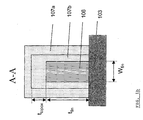
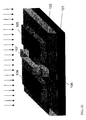
- Figure 1 shows (a) a isometric view of a prior art FinFET device formed in an SOI layer and (b) a cross-section A-A of the fin along the gate.
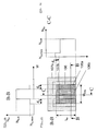
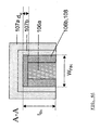
- Figure 2 shows a schematic cross section (b) of a dual gate illustrating the lowly doped and highly doped regions while (a) shows the dopant profile along line B-B.
- Figure 3 shows a schematic cross section (b) of a triple gate semiconductor device illustrating the lowly doped and highly doped regions while (a) shows the dopant profile along line B-B and (c) shows the dopant profile along line C-C.
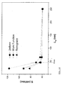
- Figure 4 shows a comparison between 3 alternative FinFET devices, each having a threshold voltage of 100mV the devices having (i) uniform doping of the fin, (ii) retrograde doping according to the present invention (according to the profile shown in Figure 4a), and (iii) work function engineering of the gate electrode material wherein (b) shows saturation current (linear scale) (c) shows saturation current (logarithmic scale) and (d) shows sub-threshold swing.
- Figure 5 shows a doping profile in the fin of a FinFET according to an embodiment of the invention.
- Figure 6 shows an alternative FinFET device according to an embodiment of the invention, wherein the device is illustrated in schematic cross-sections (a) showing a patterned fin with higher doped body, (b) showing the formation of the lowly doped surface layer enveloping at least the higher doped body of the device, (c) showing the doping of the source and drain while using the gate as a mask to protecting the channel (s) from the implantation, and (d) showing a cross-section A-A of the device.
- a semiconductor device comprising at least two gates.
- the body of this semiconductor device (e.g., the volume between these two gates) is non-uniformly doped. From the interface between the body and each gate towards the bulk of the body, the dopant concentration varies from a low value to a higher value.
- H.-S. Wong discloses various types of multi-gate devices. In figure 14, 15 and 17 of this paper, alternative orientations of such a double or triple gate device are depicted with the corresponding process sequences being detailed in pages 146 to 152. This paper is hereby incorporated by reference in its entirety.
- a FinFET device will be used to illustrate the various embodiments of the invention. However, the present invention is not limited to this type of multi-gate device.
- FIG. 1a shows a prior art FinFET device.
- a FinFET device In a semiconductor layer (102) on a substrate (101) a FinFET device, and optionally other semiconductor devices, is formed.
- the substrate itself can be a semiconductor substrate, e.g. silicon.
- An insulating layer (103) can be formed on top of this substrate (101) to insulate the semiconductor layer (102) from the substrate (101). This way e.g. a silicon-on-insulator (SOI) or a germanium-on-insulator (GeOI) substrate is formed.
- the FinFET device as shown in figure 1a comprises a source (104) and a drain (105) region connected by a fin (106), located in between this source and drain region.
- the fin (106) will constitute the body of this multi-gate device.
- the three elements (104, 105, 106) can be formed in a single layer of semiconductor material or in different layers of this semiconductor material.
- a channel of the FinFET will be that part of the fin (106) which is covered by and, depending on the thickness of the gate dielectric, under electrical control of the corresponding gate (107).
- FIG. 1b A cross-section along the gate (107) of the FinFET shown in figure 1a is given in figure 1b, illustrating the surrounding of the fin (106) at both sidewalls as well on the top by the gate (107), comprising a gate dielectric (107a) and a gate electrode layer (107b).
- a thick gate dielectric (t topox ) on top of the fin a double gate is obtained in which inversion occurs along the upstanding sidewalls of the fin (shown in figure 1b), while for a thin top gate dielectric inversion of the top channel can also occur in the top surface of the fin.
- Methods for forming FinFET devices are known in the art.
- the threshold voltage must be adjusted such that other device parameters, saturation current, leakage current, sub-threshold slope, threshold voltage roll-off are not degraded.
- Exemplary embodiments of the present invention propose to form a retrograde doped channel.
- retrograde is meant that the doping of the fin is low at the surface of the fin, but increases towards the bulk of the fin. This way a high surface mobility of the carriers can be obtained because ionized impurity scattering is reduced, while the higher bulk concentration offers a way to tune the threshold voltage of the device.
- polysilicon can still be used as gate material (107) as was the case for the classical MOS device, but also novel gate materials, such as metals, can be used. In the latter case, the bulk doping offers an additional degree of freedom for obtaining the desired threshold voltage next to the tuning of the work function of the gate electrode material.
- Figure 2 shows, for a schematic cross-section of the FinFET along line A-A (figure 2b), an example of such retrograde doping profile (figure 2a).
- the surface dopant level has a constant value N surface over a depth d w into the fin and a higher constant value N bulk in the bulk of the fin over a distance W fin -2 d w .
- N constant value
- W fin -2 d w constant value of the fin
- FIG 2b there exists a lowly doped region (106a) near the interface between the fin (106) and the gate dielectric (107b) along each of the sidewalls of the fin.
- the dopant concentration remains constant in a vertical direction, i.e., perpendicular to the substrate (101).
- a layer (109) is present on the top of the fin (106), which layer is used to prevent formation of the lowly doped region (106a) at the top of fin (106).
- FIG. 3b shows a schematic cross-section of such a triple gate FinFET device.
- Figure 3a shows the dopant profile in horizontal direction along the section B-B. This profile is similar to the dopant profile given in figure 2a.
- Figure 3c shows the dopant profile in the fin along the line C-C.
- a lowly doped region (106a) is present along a depth d w having a low concentration N surface and a higher constant value N bulk in the bulk of the fin over a distance t fin -2d w .
- Figures 4 a-d illustrate the advantages of the invention over the prior art.
- a FinFET device having a threshold voltage of 100mV is simulated using a uniform doping profile of 3e18 cm -3 throughout the fin using work function engineering, i.e. selecting the appropriate gate material (107a) and using a retrograde dopant profile as shown in figure 4a.
- Figure 4b shows on a logarithmic scale the saturation current as function of the gate voltage.
- the sub-threshold swing of the "retrograde profile” is as low as the sub-threshold swing of the "uniform profile", but with decreasing gate length the sub-threshold swing of the "retrograde profile” becomes the smallest of all three approaches, indicating it is more useable in down scaling devices.
- a box-like profile is shown, other profiles can be envisaged within the scope of this invention.
- the doping level can decrease in various ways: linear, exponential, etc.
- the doping level can vary between the two values, first and second doping level over the complete width d w of this region (106b).
- the doping concentration decreases from the first doping level at the border of the central portion (106a) to the second doping level within the outer region (106b) from whereon it will remain constant until the edge of the fin is reached.
- charge carriers will flow mainly in this constant portion of region (106b) the carriers will be less prone to impurity scattering and a larger drive current will be obtained.
- the width d i of this constant region corresponds to the width of the inversion layer region.
- the first doping level will be in the range of 1e18 to 1e20, preferably 1e19 cm -3 .
- the second doping level will be in the range of 1e15 to 1e17, preferably 1e16 cm -3 .
- the values of the first and second doping level will depend on the threshold voltage that needs to be obtained.
- the first doping level is of the order of 1e19 cm -3 and the second doping level is of the order of 1e16 cm -3 .
- the inversion layer thickness is less than a few nanometers.
- deposition techniques are employed to form a layer enveloping the body of the device resulting in a bi-layer structure, each layer, i.e. the body and the enveloping layer, of this belayed structure having a different dopant concentration.
- This enveloping layer is at least present at these surfaces of the body (106) where conduction is to take place and upon which gates (107) will be formed.
- CVD chemical vapor deposition
- a layer (108), preferably a conformal layer is formed, overlying the fin (106) of the device.
- This layer can be in-situ doped, i.e. dopants are added to the precursors of the gas mixture from which the conformal layer is to be formed. These dopants are then incorporated into the deposited layer (108). Hence the dopant concentration of this deposited layer can be different from the dopant concentration in the initial body or as-patterned fin of the device.
- the gate dielectric (106b) will be formed and the processing of the FinFET can continue.
- the layer (108) can be formed uniformly over the wafer or can be formed in a selective way, i.e.
- the published PCT application WO 01/15220 teaches the concept of using atomic layer deposition (ALD) for forming layers on selected surfaces only, hereby incorporated by reference in its enterity.
- ALD atomic layer deposition
- the selectivity can be obtained by using layers with different surface chemistry to form selected surfaces or by pre-treating selected surfaces to block the depositing of a layer on these pre-treated surfaces.
- epitaxial layer growth is used to create a dopant gradient in the body of the device.
- a process sequence is illustrated in figure 6.
- Figure 6a shows the device after patterning the fin (106) having a width W fin .
- source (104), drain (105) and fin (106) are patterned in the same semiconductor layer (102), however the invention is not limited thereto.
- the fin (106) is implanted to a first doping level N bulk selected for the bulk of the body. In an alternative sequence, this N bulk implantation is done prior to the step of patterning the fin (106). This implantation can be done in a masked way, i.e., only implanting the fin (106) or in an unmasked way also implanting the source (104) and drain (105) or the whole of the layer (102) in which source (104), drain (105) and fin (106) are formed.
- the higher junction doping of the source (104) and drain (105), given afterwards and which is of an opposite type, will compensate this lower N bulk in these source and drain regions.
- the fin will be p-type doped using dopants such as B, BF2, while the source and drain regions will be n-type doped using dopants such as P, As.
- a sacrificial oxide is grown and afterwards removed by a wet etch.
- This sacrificial oxide will remove all damage, e.g. resulting from the patterning step, at the exposed surfaces of the fin (106).
- a layer (108) is formed enveloping the fin (106) and the source (104), drain (105) areas as is shown in figure 6b.
- This layer (108) is in-situ doped to a second dopant level N surface , which is lower than the bulk concentration N bulk .
- An additional advantage of this embodiment is that the formation of an epitaxial layer on the fin will reduce the roughness of the interface between the fin and the epitaxial layer formed thereon and, hence, improve the performance of the final device even further.
- the gate (107) is formed and source (104), drain (105) regions are implanted.
- that part of the epitaxial layer (108) enveloping the source and drain will be compensated by this counter-doping of the source and drain, while that part of this layer (108) enveloping the fin (106) which corresponds to the channel will remain as-doped as it is masked by the gate (107).
- Other process steps known to a person skilled in the art are then executed the complete the processing of the device, e.g. forming insulating layers covering the device, forming electrical contacts to contact the terminals (104, 105, 106) of the device etc.
- Figure 6d shows the cross-section A-A of the device.
- the body (106) having a first dopant level is covered at the sidewalls and at this top with a layer (108), having a second dopant level lower than the first dopant level.
- This bilayer structure is covered by the gate (107), the overlay area between the bilayer structure and the gate (107) defining the channel length Lg.
- a blocking layer will be formed on the top of the fin (106).
- this blocking layer is formed over the unpatterned semiconductor layer (102) and subsequently patterned in a region, which corresponds to the top of the fin (106).
- the fin (106) and the source region (104) and drain region (105) are patterned in the semiconductor layer (102) aligned to the patterned blocking layer (109).
- the blocking layer is deposited uniformly over the unpatterned semiconductor layer (102). Both layers, the blocking layer and the semiconductor layer (102), are patterned during the same patterning step.
- the patterned blocking layer (109) will coincide with the pattern of the source (104), drain (105) and fin (106) formed in the semiconductor layer (102).
- selective depositing process such as epitaxial layer growth or atomic layer deposition (ALD) can be applied, in which case layer (108) is only formed on the exposed surfaces of the fin (106), i.e. at the sidewalls, and not on the patterned blocking layer (109) on top of the fin (106).
Abstract
A multi-gate device in accordance with an
embodiment of the present invention comprises at least
two gates. The dopant distribution in the semiconductor
body of the device varies from a low value near the
surface of the body towards a higher value inside the
body of the device.
Description
- The present invention is related to integrated circuits and methods for manufacturing such integrated circuits. More particularly, the present invention relates to semiconductor devices with multiple gates and non-uniform doping profiles in the channel region of those devices.
- Current state-of-the-art semiconductor chips feature technology with circuit feature sizes of 180 nanometers, with components manufactured with technologies having 130 nanometer feature sizes just beginning to reach the marketplace. Industry plans are to deliver 90 nanometer technologies in the year 2004, 65 nanometers in the year 2007, 45 nanometers in the year 2010, 32 nanometers in the year 2013 and 22 nanometers in the year 2016. This schedule was set forward in the International Technology Roadmap for Semiconductors (ITRS) defined by the Semiconductor Industry Association (SIA) in 2001. The schedule translates to smaller chip dimensions earlier in time than had been previously thought. Among the main transistor scaling issues to be solved is the need for thinner gate oxides that result in a higher on-current and hence increased switching speed in semiconductor devices, a smaller off-current and lower threshold voltage to allow such gate oxide scaling, and the use of lower supply voltages, a higher channel mobility and smaller series resistance of the source/drain regions. In order to meet these forecasted stringent scaling requirements, non-classical CMOS (Complementary Metal-Oxide-Semiconductor) devices and novel materials, such as metal gate materials and high-k gate dielectrics are currently under investigation.
- One of these non-classical CMOS devices is a so-called FinFET transistor. In a FinFET, the gate at least partially envelops the channel region, contrary to the classic planar device where the gate electrode is formed in one plane on top of the channel region, where the channel region is part of the substrate. Such substrates further comprise the source and drain regions adjacent to the channel region. The idea of making a double gate transistor by using the sidewalls of a dry-etched silicon (Si) fin as conducting channels was published in 1998 by D. Hisamoto et al. in "A folded-channel MOSFET for deep-sub-tenth Micron Era" in the IEDM Technical Digest 1998 pp 1032-1034. In a FinFET, a thin gate line straddles a thin silicon channel fin. Bin Yu et al, discusses in "FinFET scaling to 10nm Gate Length" IEDM Technical Digest 8-11 December, 2002 pp 251-254 an alternative process to manufacture a FinFET device. Polysilicon was used as a gate electrode material and the channel of the device was lightly doped.
- Although a FinFET can be manufactured in a near-planar, CMOS compatible way, various issues have to be addressed in order to improve the performance of such FinFET over its planar CMOS counterpart. This respective performance of such devices is indicated by various parameters such as the sub-threshold swing (S, mV/dec), which is the variation of drive current with gate voltage for gate voltages below the threshold voltage (Vt), the maximum or saturation drive current (Ion), the off state-current or leakage current Ioff), the threshold voltage roll-off (ΔVt) expressing the dependency of the threshold voltage on channel length (Lg) and drain voltage (Vds) .
- Two approaches are currently being employed to improve the FinFET device parameters. A first approach is to increase the dopant level (Nfin) of the fin. Although this approach yields a low sub-threshold slope and a controllable threshold voltage, as inversion will occur near the surface of the fin, the carrier mobility is degraded due to ionized impurity scattering. This scattering results in a lower saturation current, which slows down the device. Also the threshold voltage roll-off will be more pronounced, as the highly doped fin will not be fully depleted.
- A second approach involves lowering the fin doping and developing a tunable work-function gate technology. Yang-Kyu Choi et al in "FinFET Process Refinements for Improved Mobility and Gate Work Function Engineering" in IEDM 2002 Digest outline this approach. International, 8-11 Dec, 2002, p 259-262. Apart from forming a high quality interface between the fin and the gate dielectric, the mobility of the carriers can be improved by lowly doping the fin resulting in less ionized impurity scattering and hence in a larger saturation current. A lowly doped fin also offers the advantage of increasing the immunity of the threshold voltage to fluctuations in the dopant distribution profile. However, because of the low doping of the fin, the threshold voltage is determined by the work function of the gate electrode, which must then be carefully selected in order to obtain the desired threshold voltage for either n-type or p-type FinFETs. This approach is also cumbersome, as only a limited selection of materials is available, thereby still requiring additional efforts to tune the work function of these materials to the desired value. The introduction of such materials adds to the manufacturing process complexity. The low doping of the fin also results in a higher sub-threshold slope and consequently in a larger leakage current and a larger power consumption as is disclosed in "A Comprehensive Model Analytical Sub-threshold Swing (S) Model for Double-gate MOSFETs" by Qiang Chen et al, in IEEE Transactions on Electronic Devices, Vol. 49, No. 6, June 2002, p 1086.
- Therefore an aim of the present invention is to overcome the problems of the prior art and to achieve improved performance of a FinFET. Another aim of the present invention is to tune the threshold voltage of the FinFET without degrading other device parameters such as sub-threshold slope, saturation current, leakage current and threshold voltage roll-off.
- In a first aspect of the invention a multi-gate semiconductor device is disclosed comprising a source region and a drain region, a semiconductor body in-between which connects the source region and the drain region, a gate electrode at least at two sides of said body, wherein the semiconductor body comprises a first region having a first dopant level and a second region in-between the gate electrode and the first region, this second region having a second dopant level lower than the first doping level. This multi-gate semiconductor device may comprise a FinFET device wherein the body is the fin of the FinFET device. In certain embodiments, the first dopant level remains constant over the first region. In another embodiment, the second dopant level remains constant over the second region. In another embodiment, the dopant concentration in the second region decreases from the first dopant level to the second dopant level within the second region.
- In a second aspect of the invention a method is disclosed for manufacturing a retrograde doped multigate device according to the first aspect of the invention. In an exemplary embodiment a method for manufacturing a FinFET according to the present invention is disclosed. This method comprises providing a substrate, the substrate comprising a source, a drain and a fin connecting said source and said drain, said fin having a first dopant level, and forming a layer, at least at the exposed surfaces of the fin, said layer having a dopant level lower than said first dopant level.
- These as well as other aspects and advantages will become apparent to those of ordinary skill in the art by reading the following detailed description, with appropriate reference to the accompanying drawings.
- The appended drawings are intended to illustrate some aspects and embodiments of the present invention. Devices in the drawings are depicted in a simplified way for reason of clarity. Not all alternatives and options are shown and, therefore, the invention is not limited in scope by the drawings. It is noted that like reference numerals are employed to reference analogous parts of the various drawings, in which:
- Figure 1 shows (a) a isometric view of a prior art FinFET device formed in an SOI layer and (b) a cross-section A-A of the fin along the gate.
- Figure 2 shows a schematic cross section (b) of a dual gate illustrating the lowly doped and highly doped regions while (a) shows the dopant profile along line B-B.
- Figure 3 shows a schematic cross section (b) of a triple gate semiconductor device illustrating the lowly doped and highly doped regions while (a) shows the dopant profile along line B-B and (c) shows the dopant profile along line C-C.
- Figure 4 shows a comparison between 3 alternative FinFET devices, each having a threshold voltage of 100mV the devices having (i) uniform doping of the fin, (ii) retrograde doping according to the present invention (according to the profile shown in Figure 4a), and (iii) work function engineering of the gate electrode material wherein (b) shows saturation current (linear scale) (c) shows saturation current (logarithmic scale) and (d) shows sub-threshold swing.
- Figure 5 shows a doping profile in the fin of a FinFET according to an embodiment of the invention.
- Figure 6 shows an alternative FinFET device according to an embodiment of the invention, wherein the device is illustrated in schematic cross-sections (a) showing a patterned fin with higher doped body, (b) showing the formation of the lowly doped surface layer enveloping at least the higher doped body of the device, (c) showing the doping of the source and drain while using the gate as a mask to protecting the channel (s) from the implantation, and (d) showing a cross-section A-A of the device.
- In relation to the drawings, the present invention is described in detail in the following detailed description. It will be apparent, however, to a person skilled in the art that numerous other equivalent embodiments or other ways of practicing the present invention exist.
- In a first aspect of the invention, a semiconductor device comprising at least two gates is disclosed. The body of this semiconductor device (e.g., the volume between these two gates) is non-uniformly doped. From the interface between the body and each gate towards the bulk of the body, the dopant concentration varies from a low value to a higher value. In his article "Beyond the Conventional Transistor", published in IBM Journal of Research & Development, Vol. 46, No. 23 2002, H.-S. Wong discloses various types of multi-gate devices. In figure 14, 15 and 17 of this paper, alternative orientations of such a double or triple gate device are depicted with the corresponding process sequences being detailed in pages 146 to 152. This paper is hereby incorporated by reference in its entirety. For the purpose of teaching the invention, a FinFET device will be used to illustrate the various embodiments of the invention. However, the present invention is not limited to this type of multi-gate device.
- Figure 1a shows a prior art FinFET device. In a semiconductor layer (102) on a substrate (101) a FinFET device, and optionally other semiconductor devices, is formed. The substrate itself can be a semiconductor substrate, e.g. silicon. An insulating layer (103) can be formed on top of this substrate (101) to insulate the semiconductor layer (102) from the substrate (101). This way e.g. a silicon-on-insulator (SOI) or a germanium-on-insulator (GeOI) substrate is formed. The FinFET device as shown in figure 1a comprises a source (104) and a drain (105) region connected by a fin (106), located in between this source and drain region. The fin (106) will constitute the body of this multi-gate device. Depending on the process flow, the three elements (104, 105, 106) can be formed in a single layer of semiconductor material or in different layers of this semiconductor material. A gate (107), comprising a gate dielectric and a gate electrode layer, is formed as to overly the fin (106) at three sides: the top surface and the two sides. A channel of the FinFET will be that part of the fin (106) which is covered by and, depending on the thickness of the gate dielectric, under electrical control of the corresponding gate (107).
- A cross-section along the gate (107) of the FinFET shown in figure 1a is given in figure 1b, illustrating the surrounding of the fin (106) at both sidewalls as well on the top by the gate (107), comprising a gate dielectric (107a) and a gate electrode layer (107b). In case of a thick gate dielectric (ttopox) on top of the fin, a double gate is obtained in which inversion occurs along the upstanding sidewalls of the fin (shown in figure 1b), while for a thin top gate dielectric inversion of the top channel can also occur in the top surface of the fin. Methods for forming FinFET devices are known in the art. An example is disclosed in "High-Performance Symmetric-Gate and CMOS Compatible Vt Asymmetric-Gate FinFET devices" in IEDM Technical Digest 2001 pp 437-440, by J. Kedzierski et al. wherein the source/drain regions or pads, as they are labeled there, are formed together with the fin channel in the SOI layer using optical lithography and a hard mask trimming technique.
- To achieve optimum performance from the device, the threshold voltage must be adjusted such that other device parameters, saturation current, leakage current, sub-threshold slope, threshold voltage roll-off are not degraded. Exemplary embodiments of the present invention propose to form a retrograde doped channel. With retrograde is meant that the doping of the fin is low at the surface of the fin, but increases towards the bulk of the fin. This way a high surface mobility of the carriers can be obtained because ionized impurity scattering is reduced, while the higher bulk concentration offers a way to tune the threshold voltage of the device. In this respect, polysilicon can still be used as gate material (107) as was the case for the classical MOS device, but also novel gate materials, such as metals, can be used. In the latter case, the bulk doping offers an additional degree of freedom for obtaining the desired threshold voltage next to the tuning of the work function of the gate electrode material.
- Figure 2 shows, for a schematic cross-section of the FinFET along line A-A (figure 2b), an example of such retrograde doping profile (figure 2a). In this example, the surface dopant level has a constant value Nsurface over a depth dw into the fin and a higher constant value Nbulk in the bulk of the fin over a distance Wfin-2 dw. In case of a double gate FinFET, it might be sufficient to only have a dopant gradient in the fin along the horizontal direction. As shown in figure 2b, there exists a lowly doped region (106a) near the interface between the fin (106) and the gate dielectric (107b) along each of the sidewalls of the fin. In this example, the dopant concentration remains constant in a vertical direction, i.e., perpendicular to the substrate (101). Optionally a layer (109) is present on the top of the fin (106), which layer is used to prevent formation of the lowly doped region (106a) at the top of fin (106).
- In case a triple gate FinFET is formed, i.e. by having a thin dielectric on top of the fin, then preferably also a dopant gradient is formed in the vertical direction. Figure 3b shows a schematic cross-section of such a triple gate FinFET device. Figure 3a shows the dopant profile in horizontal direction along the section B-B. This profile is similar to the dopant profile given in figure 2a. In a triple gate device, conduction will not only occur along the sidewalls of the fin, but also at the top surface of the fin parallel with the substrate (101). Figure 3c shows the dopant profile in the fin along the line C-C. From the interface between the fin and the gate dielectric, a lowly doped region (106a) is present along a depth dw having a low concentration Nsurface and a higher constant value Nbulk in the bulk of the fin over a distance tfin-2dw. Figures 4 a-d illustrate the advantages of the invention over the prior art. A FinFET device having a threshold voltage of 100mV is simulated using a uniform doping profile of 3e18 cm-3 throughout the fin using work function engineering, i.e. selecting the appropriate gate material (107a) and using a retrograde dopant profile as shown in figure 4a. Figure 4b shows on a logarithmic scale the saturation current as function of the gate voltage. At zero gate voltage, the leakage current in saturation region for each alternative can be seen. The "work function" alternative has the largest leakage current, while the "retrograde profile" performs as well as the "uniform profile". Figure 4c shows the saturation current as function of the gate voltage. At maximum gate voltage the drive current for each alternative can be seen. The "uniform profile" alternative has the lowest drive current, while the "retrograde profile" performs as well as the "work function" alternative. In figure 4d the sub-threshold swing as function of the gate length Lg is given for the three approaches. For a gate length of 45 nm, which is the device used in figure 4b and 4c, having a threshold voltage of 100 mV, the sub-threshold swing of the "retrograde profile" is as low as the sub-threshold swing of the "uniform profile", but with decreasing gate length the sub-threshold swing of the "retrograde profile" becomes the smallest of all three approaches, indicating it is more useable in down scaling devices.
- Whereas in figures 2a, 3a and 3c a box-like profile is shown, other profiles can be envisaged within the scope of this invention. One could use a profile with a central portion (106b) of the fin having a first constant doping level, and a outer portion (106b) of the fin wherein the doping level decreases to a second doping level, being less than the first doping level. Within this border region (106b), the doping level can decrease in various ways: linear, exponential, etc. The doping level can vary between the two values, first and second doping level over the complete width dw of this region (106b). In a preferred embodiment, illustrated in figure 5, the doping concentration decreases from the first doping level at the border of the central portion (106a) to the second doping level within the outer region (106b) from whereon it will remain constant until the edge of the fin is reached. As during operation charge carriers will flow mainly in this constant portion of region (106b) the carriers will be less prone to impurity scattering and a larger drive current will be obtained. Preferably the width di of this constant region corresponds to the width of the inversion layer region. Typically the first doping level will be in the range of 1e18 to 1e20, preferably 1e19 cm-3. The second doping level will be in the range of 1e15 to 1e17, preferably 1e16 cm-3. The values of the first and second doping level will depend on the threshold voltage that needs to be obtained. In a preferred embodiment of the invention, the first doping level is of the order of 1e19 cm-3 and the second doping level is of the order of 1e16 cm-3. The fin has a total thickness of about Wfin = 45nm, with a central portion (106a) of about 25nm and an outer region (106b) of about dw = 10nm per side. Typically, the inversion layer thickness is less than a few nanometers.
- In a second aspect of the invention, methods are disclosed to manufacture such a multi-gate device comprising an increasing dopant profile from each gate on towards the bulk of the device.
- In one embodiment of the second aspect layer, deposition techniques are employed to form a layer enveloping the body of the device resulting in a bi-layer structure, each layer, i.e. the body and the enveloping layer, of this belayed structure having a different dopant concentration. This enveloping layer is at least present at these surfaces of the body (106) where conduction is to take place and upon which gates (107) will be formed. Various techniques exist in semiconductor technology to deposit layers. One of these techniques is chemical vapor deposition (CVD), which covers a wide range of processes: epitaxial layer growth, atomic layer CVD, plasma enhanced CVD, all of which are known by a person skilled in the art. Prior to the step of depositing the gate dielectric (106b), a layer (108), preferably a conformal layer is formed, overlying the fin (106) of the device. This layer can be in-situ doped, i.e. dopants are added to the precursors of the gas mixture from which the conformal layer is to be formed. These dopants are then incorporated into the deposited layer (108). Hence the dopant concentration of this deposited layer can be different from the dopant concentration in the initial body or as-patterned fin of the device. On top of this deposited layer the gate dielectric (106b) will be formed and the processing of the FinFET can continue. The layer (108) can be formed uniformly over the wafer or can be formed in a selective way, i.e. only on the exposed surfaces of the fin (106), as the top surface of the fin (106) might optionally by covered with a layer or treated as to not react with the species of the deposition atmosphere. This selective deposition can be obtained by using epitaxial layer growth or selective ALD, both techniques are known by a person skilled in the art. Wolf and Tauber teaches in "silicon processing for the VLSI era, volume I - Process Technology", 2nd Edition, Lattice Press, on page 225-226 the concept of epitaxial growth, on page 236 the concept of in-situ doping such layers (section 7.4.3) and in section 7.7 on page 245-247 the concept of selective epitaxial growth. The published PCT application WO 01/15220 teaches the concept of using atomic layer deposition (ALD) for forming layers on selected surfaces only, hereby incorporated by reference in its enterity. The selectivity can be obtained by using layers with different surface chemistry to form selected surfaces or by pre-treating selected surfaces to block the depositing of a layer on these pre-treated surfaces.
- In a preferred embodiment of this second aspect, epitaxial layer growth is used to create a dopant gradient in the body of the device. A process sequence is illustrated in figure 6.
- Figure 6a shows the device after patterning the fin (106) having a width Wfin. In this example, source (104), drain (105) and fin (106) are patterned in the same semiconductor layer (102), however the invention is not limited thereto. The fin (106) is implanted to a first doping level Nbulk selected for the bulk of the body. In an alternative sequence, this Nbulk implantation is done prior to the step of patterning the fin (106). This implantation can be done in a masked way, i.e., only implanting the fin (106) or in an unmasked way also implanting the source (104) and drain (105) or the whole of the layer (102) in which source (104), drain (105) and fin (106) are formed. In the latter case, the higher junction doping of the source (104) and drain (105), given afterwards and which is of an opposite type, will compensate this lower Nbulk in these source and drain regions. In case electrons are to be used as carriers, the fin will be p-type doped using dopants such as B, BF2, while the source and drain regions will be n-type doped using dopants such as P, As.
- Preferably a sacrificial oxide is grown and afterwards removed by a wet etch. This sacrificial oxide will remove all damage, e.g. resulting from the patterning step, at the exposed surfaces of the fin (106). Using epitaxial layer growth, a layer (108) is formed enveloping the fin (106) and the source (104), drain (105) areas as is shown in figure 6b. This layer (108) is in-situ doped to a second dopant level Nsurface, which is lower than the bulk concentration Nbulk. An additional advantage of this embodiment is that the formation of an epitaxial layer on the fin will reduce the roughness of the interface between the fin and the epitaxial layer formed thereon and, hence, improve the performance of the final device even further.
- As shown in figure 6c, the gate (107) is formed and source (104), drain (105) regions are implanted. As explained above, that part of the epitaxial layer (108) enveloping the source and drain will be compensated by this counter-doping of the source and drain, while that part of this layer (108) enveloping the fin (106) which corresponds to the channel will remain as-doped as it is masked by the gate (107). Other process steps known to a person skilled in the art are then executed the complete the processing of the device, e.g. forming insulating layers covering the device, forming electrical contacts to contact the terminals (104, 105, 106) of the device etc.
- Figure 6d shows the cross-section A-A of the device. The body (106) having a first dopant level is covered at the sidewalls and at this top with a layer (108), having a second dopant level lower than the first dopant level. This bilayer structure is covered by the gate (107), the overlay area between the bilayer structure and the gate (107) defining the channel length Lg.
- In case a double gate is to be formed as shown in figure 2b, the above process only need some minor modifications. Prior to the step of forming the layer (108), as illustrated in figure 6b, a blocking layer will be formed on the top of the fin (106). A person skilled in the art will appreciate that this blocking layer is formed over the unpatterned semiconductor layer (102) and subsequently patterned in a region, which corresponds to the top of the fin (106). Afterwards the fin (106) and the source region (104) and drain region (105) are patterned in the semiconductor layer (102) aligned to the patterned blocking layer (109). In an alternative method the blocking layer is deposited uniformly over the unpatterned semiconductor layer (102). Both layers, the blocking layer and the semiconductor layer (102), are patterned during the same patterning step. In this case the patterned blocking layer (109) will coincide with the pattern of the source (104), drain (105) and fin (106) formed in the semiconductor layer (102). As discussed above selective depositing process, such as epitaxial layer growth or atomic layer deposition (ALD) can be applied, in which case layer (108) is only formed on the exposed surfaces of the fin (106), i.e. at the sidewalls, and not on the patterned blocking layer (109) on top of the fin (106).
- Exemplary embodiments of the present invention have thus been illustrated and described. It will be understood, however, that changes and modifications may be made to the invention as described without deviating from the spirit and scope of the invention, as defined by the following claims.
Claims (8)
- A multi-gate semiconductor device comprising:characterized in thata source region (104) ;a drain region (105);a semiconductor body (106) in-between said source region (104) and drain region (105), and connecting said source region (104) and said drain region (105); anda gate structure (107) formed at at least two sides of said body (106) ;
said semiconductor body (106) comprises a first region (106b) having a first dopant level and a second region (106a), in-between said gate structure (107) and said first region (106b), having a second dopant level lower than said first doping level. - The device of claim 1 wherein said multi-gate semiconductor device is a FinFET device and said semiconductor body (106) comprises the fin of said FinFET device.
- The device of claim 1 or 2 wherein said first dopant level remains constant over said first region (106b) .
- The device of any foregoing claim wherein said second dopant level remains constant over said second region (106a).
- The device of claim 1, 2 or 3 wherein the dopant concentration in said second region (106b) decreases from said first dopant level to said second dopant level within said second region.
- A method for manufacturing a retrograde FinFET, comprising:characterized in thatproviding a substrate (101), wherein the substrate comprises:a source (104);a drain (105); anda fin (106) connecting said source (104) and said drain (105), wherein said fin (106) has a first dopant level; and
it further comprises forming a layer (108), at least on the exposed surfaces of the fin (106), said layer having a dopant level lower than said first dopant level. - A method as claimed in claim 6 wherein the step of forming a layer (108) includes in-situ doping of the layer (108).
- A method as recited in claim 6 or 7 wherein said said layer (108) is formed using epitaxial layer growth.
Priority Applications (4)
| Application Number | Priority Date | Filing Date | Title |
|---|---|---|---|
| EP03447238A EP1519421A1 (en) | 2003-09-25 | 2003-09-25 | Multiple gate semiconductor device and method for forming same |
| EP04447178.7A EP1498958B1 (en) | 2003-07-18 | 2004-07-16 | Method for forming a mutiple gate semiconductor device |
| US10/893,185 US7202517B2 (en) | 2003-07-18 | 2004-07-16 | Multiple gate semiconductor device and method for forming same |
| JP2004210161A JP2005045245A (en) | 2003-07-18 | 2004-07-16 | Multiple gate semiconductor device and method of forming the same |
Applications Claiming Priority (1)
| Application Number | Priority Date | Filing Date | Title |
|---|---|---|---|
| EP03447238A EP1519421A1 (en) | 2003-09-25 | 2003-09-25 | Multiple gate semiconductor device and method for forming same |
Publications (1)
| Publication Number | Publication Date |
|---|---|
| EP1519421A1 true EP1519421A1 (en) | 2005-03-30 |
Family
ID=34178727
Family Applications (1)
| Application Number | Title | Priority Date | Filing Date |
|---|---|---|---|
| EP03447238A Withdrawn EP1519421A1 (en) | 2003-07-18 | 2003-09-25 | Multiple gate semiconductor device and method for forming same |
Country Status (2)
| Country | Link |
|---|---|
| US (1) | US7202517B2 (en) |
| EP (1) | EP1519421A1 (en) |
Cited By (2)
| Publication number | Priority date | Publication date | Assignee | Title |
|---|---|---|---|---|
| US7419866B2 (en) | 2006-03-15 | 2008-09-02 | Freescale Semiconductor, Inc. | Process of forming an electronic device including a semiconductor island over an insulating layer |
| US7456055B2 (en) | 2006-03-15 | 2008-11-25 | Freescale Semiconductor, Inc. | Process for forming an electronic device including semiconductor fins |
Families Citing this family (105)
| Publication number | Priority date | Publication date | Assignee | Title |
|---|---|---|---|---|
| US6946377B2 (en) | 2003-10-29 | 2005-09-20 | Texas Instruments Incorporated | Multiple-gate MOSFET device with lithography independent silicon body thickness and methods for fabricating the same |
| US7091566B2 (en) * | 2003-11-20 | 2006-08-15 | International Business Machines Corp. | Dual gate FinFet |
| US7253043B2 (en) * | 2005-06-14 | 2007-08-07 | Texas Instruments Incorporated | Short channel semiconductor device fabrication |
| US20070090408A1 (en) * | 2005-09-29 | 2007-04-26 | Amlan Majumdar | Narrow-body multiple-gate FET with dominant body transistor for high performance |
| US7446352B2 (en) | 2006-03-09 | 2008-11-04 | Tela Innovations, Inc. | Dynamic array architecture |
| US7908578B2 (en) | 2007-08-02 | 2011-03-15 | Tela Innovations, Inc. | Methods for designing semiconductor device with dynamic array section |
| US9035359B2 (en) | 2006-03-09 | 2015-05-19 | Tela Innovations, Inc. | Semiconductor chip including region including linear-shaped conductive structures forming gate electrodes and having electrical connection areas arranged relative to inner region between transistors of different types and associated methods |
| US8839175B2 (en) | 2006-03-09 | 2014-09-16 | Tela Innovations, Inc. | Scalable meta-data objects |
| US9009641B2 (en) | 2006-03-09 | 2015-04-14 | Tela Innovations, Inc. | Circuits with linear finfet structures |
| US7956421B2 (en) | 2008-03-13 | 2011-06-07 | Tela Innovations, Inc. | Cross-coupled transistor layouts in restricted gate level layout architecture |
| US8245180B2 (en) | 2006-03-09 | 2012-08-14 | Tela Innovations, Inc. | Methods for defining and using co-optimized nanopatterns for integrated circuit design and apparatus implementing same |
| US9563733B2 (en) | 2009-05-06 | 2017-02-07 | Tela Innovations, Inc. | Cell circuit and layout with linear finfet structures |
| US7763534B2 (en) | 2007-10-26 | 2010-07-27 | Tela Innovations, Inc. | Methods, structures and designs for self-aligning local interconnects used in integrated circuits |
| US8653857B2 (en) | 2006-03-09 | 2014-02-18 | Tela Innovations, Inc. | Circuitry and layouts for XOR and XNOR logic |
| US8225239B2 (en) | 2006-03-09 | 2012-07-17 | Tela Innovations, Inc. | Methods for defining and utilizing sub-resolution features in linear topology |
| US8247846B2 (en) | 2006-03-09 | 2012-08-21 | Tela Innovations, Inc. | Oversized contacts and vias in semiconductor chip defined by linearly constrained topology |
| US9230910B2 (en) | 2006-03-09 | 2016-01-05 | Tela Innovations, Inc. | Oversized contacts and vias in layout defined by linearly constrained topology |
| US8658542B2 (en) | 2006-03-09 | 2014-02-25 | Tela Innovations, Inc. | Coarse grid design methods and structures |
| US8225261B2 (en) | 2006-03-09 | 2012-07-17 | Tela Innovations, Inc. | Methods for defining contact grid in dynamic array architecture |
| US8541879B2 (en) | 2007-12-13 | 2013-09-24 | Tela Innovations, Inc. | Super-self-aligned contacts and method for making the same |
| US8214778B2 (en) | 2007-08-02 | 2012-07-03 | Tela Innovations, Inc. | Methods for cell phasing and placement in dynamic array architecture and implementation of the same |
| US8448102B2 (en) | 2006-03-09 | 2013-05-21 | Tela Innovations, Inc. | Optimizing layout of irregular structures in regular layout context |
| US7646071B2 (en) | 2006-05-31 | 2010-01-12 | Intel Corporation | Asymmetric channel doping for improved memory operation for floating body cell (FBC) memory |
| US20080111185A1 (en) * | 2006-11-13 | 2008-05-15 | International Business Machines Corporation | Asymmetric multi-gated transistor and method for forming |
| US8286107B2 (en) | 2007-02-20 | 2012-10-09 | Tela Innovations, Inc. | Methods and systems for process compensation technique acceleration |
| US8667443B2 (en) | 2007-03-05 | 2014-03-04 | Tela Innovations, Inc. | Integrated circuit cell library for multiple patterning |
| US8453094B2 (en) | 2008-01-31 | 2013-05-28 | Tela Innovations, Inc. | Enforcement of semiconductor structure regularity for localized transistors and interconnect |
| US7939443B2 (en) | 2008-03-27 | 2011-05-10 | Tela Innovations, Inc. | Methods for multi-wire routing and apparatus implementing same |
| DE102008030853B4 (en) * | 2008-06-30 | 2014-04-30 | Globalfoundries Dresden Module One Limited Liability Company & Co. Kg | Three-dimensional transistor with a dual-channel configuration |
| US9122832B2 (en) | 2008-08-01 | 2015-09-01 | Tela Innovations, Inc. | Methods for controlling microloading variation in semiconductor wafer layout and fabrication |
| US9054194B2 (en) | 2009-04-29 | 2015-06-09 | Taiwan Semiconductor Manufactruing Company, Ltd. | Non-planar transistors and methods of fabrication thereof |
| US7999332B2 (en) * | 2009-05-14 | 2011-08-16 | International Business Machines Corporation | Asymmetric semiconductor devices and method of fabricating |
| US8421162B2 (en) | 2009-09-30 | 2013-04-16 | Suvolta, Inc. | Advanced transistors with punch through suppression |
| US8273617B2 (en) | 2009-09-30 | 2012-09-25 | Suvolta, Inc. | Electronic devices and systems, and methods for making and using the same |
| US8661392B2 (en) | 2009-10-13 | 2014-02-25 | Tela Innovations, Inc. | Methods for cell boundary encroachment and layouts implementing the Same |
| US8530286B2 (en) | 2010-04-12 | 2013-09-10 | Suvolta, Inc. | Low power semiconductor transistor structure and method of fabrication thereof |
| US8569128B2 (en) | 2010-06-21 | 2013-10-29 | Suvolta, Inc. | Semiconductor structure and method of fabrication thereof with mixed metal types |
| US8759872B2 (en) | 2010-06-22 | 2014-06-24 | Suvolta, Inc. | Transistor with threshold voltage set notch and method of fabrication thereof |
| US8816392B2 (en) * | 2010-07-01 | 2014-08-26 | Institute of Microelectronics, Chinese Academy of Sciences | Semiconductor device having gate structures to reduce the short channel effects |
| US8377783B2 (en) | 2010-09-30 | 2013-02-19 | Suvolta, Inc. | Method for reducing punch-through in a transistor device |
| US9159627B2 (en) | 2010-11-12 | 2015-10-13 | Tela Innovations, Inc. | Methods for linewidth modification and apparatus implementing the same |
| US8404551B2 (en) | 2010-12-03 | 2013-03-26 | Suvolta, Inc. | Source/drain extension control for advanced transistors |
| US9385050B2 (en) | 2011-01-06 | 2016-07-05 | Globalfoundries Inc. | Structure and method to fabricate resistor on finFET processes |
| US8461875B1 (en) | 2011-02-18 | 2013-06-11 | Suvolta, Inc. | Digital circuits having improved transistors, and methods therefor |
| US8525271B2 (en) | 2011-03-03 | 2013-09-03 | Suvolta, Inc. | Semiconductor structure with improved channel stack and method for fabrication thereof |
| US8400219B2 (en) | 2011-03-24 | 2013-03-19 | Suvolta, Inc. | Analog circuits having improved transistors, and methods therefor |
| US8748270B1 (en) | 2011-03-30 | 2014-06-10 | Suvolta, Inc. | Process for manufacturing an improved analog transistor |
| US8999861B1 (en) | 2011-05-11 | 2015-04-07 | Suvolta, Inc. | Semiconductor structure with substitutional boron and method for fabrication thereof |
| US8796048B1 (en) | 2011-05-11 | 2014-08-05 | Suvolta, Inc. | Monitoring and measurement of thin film layers |
| US8811068B1 (en) | 2011-05-13 | 2014-08-19 | Suvolta, Inc. | Integrated circuit devices and methods |
| US8569156B1 (en) | 2011-05-16 | 2013-10-29 | Suvolta, Inc. | Reducing or eliminating pre-amorphization in transistor manufacture |
| US8735987B1 (en) | 2011-06-06 | 2014-05-27 | Suvolta, Inc. | CMOS gate stack structures and processes |
| US8995204B2 (en) | 2011-06-23 | 2015-03-31 | Suvolta, Inc. | Circuit devices and methods having adjustable transistor body bias |
| US8629016B1 (en) | 2011-07-26 | 2014-01-14 | Suvolta, Inc. | Multiple transistor types formed in a common epitaxial layer by differential out-diffusion from a doped underlayer |
| US8748986B1 (en) | 2011-08-05 | 2014-06-10 | Suvolta, Inc. | Electronic device with controlled threshold voltage |
| KR101891373B1 (en) | 2011-08-05 | 2018-08-24 | 엠아이이 후지쯔 세미컨덕터 리미티드 | Semiconductor devices having fin structures and fabrication methods thereof |
| US8614128B1 (en) | 2011-08-23 | 2013-12-24 | Suvolta, Inc. | CMOS structures and processes based on selective thinning |
| US8645878B1 (en) | 2011-08-23 | 2014-02-04 | Suvolta, Inc. | Porting a circuit design from a first semiconductor process to a second semiconductor process |
| US8890207B2 (en) * | 2011-09-06 | 2014-11-18 | Taiwan Semiconductor Manufacturing Company, Ltd. | FinFET design controlling channel thickness |
| US8713511B1 (en) | 2011-09-16 | 2014-04-29 | Suvolta, Inc. | Tools and methods for yield-aware semiconductor manufacturing process target generation |
| US9236466B1 (en) | 2011-10-07 | 2016-01-12 | Mie Fujitsu Semiconductor Limited | Analog circuits having improved insulated gate transistors, and methods therefor |
| US8772149B2 (en) | 2011-10-19 | 2014-07-08 | International Business Machines Corporation | FinFET structure and method to adjust threshold voltage in a FinFET structure |
| US9040399B2 (en) * | 2011-10-27 | 2015-05-26 | International Business Machines Corporation | Threshold voltage adjustment for thin body MOSFETs |
| US8895327B1 (en) | 2011-12-09 | 2014-11-25 | Suvolta, Inc. | Tipless transistors, short-tip transistors, and methods and circuits therefor |
| US8819603B1 (en) | 2011-12-15 | 2014-08-26 | Suvolta, Inc. | Memory circuits and methods of making and designing the same |
| US8883600B1 (en) | 2011-12-22 | 2014-11-11 | Suvolta, Inc. | Transistor having reduced junction leakage and methods of forming thereof |
| US8599623B1 (en) | 2011-12-23 | 2013-12-03 | Suvolta, Inc. | Circuits and methods for measuring circuit elements in an integrated circuit device |
| US8970289B1 (en) | 2012-01-23 | 2015-03-03 | Suvolta, Inc. | Circuits and devices for generating bi-directional body bias voltages, and methods therefor |
| US8877619B1 (en) | 2012-01-23 | 2014-11-04 | Suvolta, Inc. | Process for manufacture of integrated circuits with different channel doping transistor architectures and devices therefrom |
| US9093550B1 (en) | 2012-01-31 | 2015-07-28 | Mie Fujitsu Semiconductor Limited | Integrated circuits having a plurality of high-K metal gate FETs with various combinations of channel foundation structure and gate stack structure and methods of making same |
| US9406567B1 (en) | 2012-02-28 | 2016-08-02 | Mie Fujitsu Semiconductor Limited | Method for fabricating multiple transistor devices on a substrate with varying threshold voltages |
| KR101894221B1 (en) * | 2012-03-21 | 2018-10-04 | 삼성전자주식회사 | Field effect transistor and semiconductor device including the same |
| CN103325833B (en) * | 2012-03-21 | 2018-08-07 | 三星电子株式会社 | Field-effect transistor and semiconductor devices and integrated circuit device including it |
| US8863064B1 (en) | 2012-03-23 | 2014-10-14 | Suvolta, Inc. | SRAM cell layout structure and devices therefrom |
| US8802535B2 (en) | 2012-05-02 | 2014-08-12 | International Business Machines Corporation | Doped core trigate FET structure and method |
| US9299698B2 (en) | 2012-06-27 | 2016-03-29 | Mie Fujitsu Semiconductor Limited | Semiconductor structure with multiple transistors having various threshold voltages |
| US8673731B2 (en) | 2012-08-20 | 2014-03-18 | International Business Machines Corporation | Techniques for gate workfunction engineering to reduce short channel effects in planar CMOS devices |
| US8669167B1 (en) * | 2012-08-28 | 2014-03-11 | International Business Machines Corporation | Techniques for metal gate workfunction engineering to enable multiple threshold voltage FINFET devices |
| US8637955B1 (en) | 2012-08-31 | 2014-01-28 | Suvolta, Inc. | Semiconductor structure with reduced junction leakage and method of fabrication thereof |
| US9112057B1 (en) | 2012-09-18 | 2015-08-18 | Mie Fujitsu Semiconductor Limited | Semiconductor devices with dopant migration suppression and method of fabrication thereof |
| US9041126B2 (en) | 2012-09-21 | 2015-05-26 | Mie Fujitsu Semiconductor Limited | Deeply depleted MOS transistors having a screening layer and methods thereof |
| US20140103437A1 (en) * | 2012-10-15 | 2014-04-17 | Gold Standard Simulations Ltd. | Random Doping Fluctuation Resistant FinFET |
| US9177820B2 (en) * | 2012-10-24 | 2015-11-03 | Globalfoundries U.S. 2 Llc | Sub-lithographic semiconductor structures with non-constant pitch |
| CN104854698A (en) | 2012-10-31 | 2015-08-19 | 三重富士通半导体有限责任公司 | Dram-type device with low variation transistor peripheral circuits, and related methods |
| US8816754B1 (en) | 2012-11-02 | 2014-08-26 | Suvolta, Inc. | Body bias circuits and methods |
| US9093997B1 (en) | 2012-11-15 | 2015-07-28 | Mie Fujitsu Semiconductor Limited | Slew based process and bias monitors and related methods |
| US9070477B1 (en) | 2012-12-12 | 2015-06-30 | Mie Fujitsu Semiconductor Limited | Bit interleaved low voltage static random access memory (SRAM) and related methods |
| US8847324B2 (en) * | 2012-12-17 | 2014-09-30 | Synopsys, Inc. | Increasing ION /IOFF ratio in FinFETs and nano-wires |
| US9112484B1 (en) | 2012-12-20 | 2015-08-18 | Mie Fujitsu Semiconductor Limited | Integrated circuit process and bias monitors and related methods |
| US9268885B1 (en) | 2013-02-28 | 2016-02-23 | Mie Fujitsu Semiconductor Limited | Integrated circuit device methods and models with predicted device metric variations |
| US8994415B1 (en) | 2013-03-01 | 2015-03-31 | Suvolta, Inc. | Multiple VDD clock buffer |
| US8988153B1 (en) | 2013-03-09 | 2015-03-24 | Suvolta, Inc. | Ring oscillator with NMOS or PMOS variation insensitivity |
| US9299801B1 (en) | 2013-03-14 | 2016-03-29 | Mie Fujitsu Semiconductor Limited | Method for fabricating a transistor device with a tuned dopant profile |
| US9449967B1 (en) | 2013-03-15 | 2016-09-20 | Fujitsu Semiconductor Limited | Transistor array structure |
| US9112495B1 (en) | 2013-03-15 | 2015-08-18 | Mie Fujitsu Semiconductor Limited | Integrated circuit device body bias circuits and methods |
| US9478571B1 (en) | 2013-05-24 | 2016-10-25 | Mie Fujitsu Semiconductor Limited | Buried channel deeply depleted channel transistor |
| US9000536B2 (en) * | 2013-06-28 | 2015-04-07 | Taiwan Semiconductor Manufacturing Co., Ltd. | Fin field effect transistor having a highly doped region |
| US9847404B2 (en) * | 2013-07-06 | 2017-12-19 | Semiwise Limited | Fluctuation resistant FinFET |
| US8976575B1 (en) | 2013-08-29 | 2015-03-10 | Suvolta, Inc. | SRAM performance monitor |
| KR102224525B1 (en) * | 2014-02-03 | 2021-03-08 | 삼성전자주식회사 | Layout design system, semiconductor device fabricated by using the system and method for fabricating the semiconductor device |
| JP2015177094A (en) * | 2014-03-17 | 2015-10-05 | 株式会社東芝 | semiconductor device |
| US9224736B1 (en) * | 2014-06-27 | 2015-12-29 | Taiwan Semicondcutor Manufacturing Company, Ltd. | Structure and method for SRAM FinFET device |
| US9710006B2 (en) | 2014-07-25 | 2017-07-18 | Mie Fujitsu Semiconductor Limited | Power up body bias circuits and methods |
| US9319013B2 (en) | 2014-08-19 | 2016-04-19 | Mie Fujitsu Semiconductor Limited | Operational amplifier input offset correction with transistor threshold voltage adjustment |
| US9735275B2 (en) | 2015-12-18 | 2017-08-15 | International Business Machines Corporation | Channel replacement and bimodal doping scheme for bulk finFET threshold voltage modulation with reduced performance penalty |
Citations (6)
| Publication number | Priority date | Publication date | Assignee | Title |
|---|---|---|---|---|
| EP0304811A1 (en) * | 1987-08-24 | 1989-03-01 | Asea Brown Boveri Ab | MOS transistor |
| EP0623963A1 (en) * | 1993-05-06 | 1994-11-09 | Siemens Aktiengesellschaft | MOSFET on SOI substrate |
| US20020011612A1 (en) * | 2000-07-31 | 2002-01-31 | Kabushiki Kaisha Toshiba | Semiconductor device and method for manufacturing the same |
| US6372582B1 (en) * | 1999-08-18 | 2002-04-16 | Advanced Micro Devices, Inc. | Indium retrograde channel doping for improved gate oxide reliability |
| US6383876B1 (en) * | 1997-05-06 | 2002-05-07 | Lg Semicon Co., Ltd. | MOS device having non-uniform dopant concentration and method for fabricating the same |
| US20030141569A1 (en) * | 2002-01-28 | 2003-07-31 | Fried David M. | Fin-type resistors |
Family Cites Families (9)
| Publication number | Priority date | Publication date | Assignee | Title |
|---|---|---|---|---|
| US6391785B1 (en) | 1999-08-24 | 2002-05-21 | Interuniversitair Microelektronica Centrum (Imec) | Method for bottomless deposition of barrier layers in integrated circuit metallization schemes |
| JP4044276B2 (en) * | 2000-09-28 | 2008-02-06 | 株式会社東芝 | Semiconductor device and manufacturing method thereof |
| US6475869B1 (en) | 2001-02-26 | 2002-11-05 | Advanced Micro Devices, Inc. | Method of forming a double gate transistor having an epitaxial silicon/germanium channel region |
| US6717213B2 (en) | 2001-06-29 | 2004-04-06 | Intel Corporation | Creation of high mobility channels in thin-body SOI devices |
| JP3647777B2 (en) | 2001-07-06 | 2005-05-18 | 株式会社東芝 | Method of manufacturing field effect transistor and integrated circuit element |
| US6800910B2 (en) | 2002-09-30 | 2004-10-05 | Advanced Micro Devices, Inc. | FinFET device incorporating strained silicon in the channel region |
| US7074656B2 (en) * | 2003-04-29 | 2006-07-11 | Taiwan Semiconductor Manufacturing Company, Ltd. | Doping of semiconductor fin devices |
| US7045401B2 (en) * | 2003-06-23 | 2006-05-16 | Sharp Laboratories Of America, Inc. | Strained silicon finFET device |
| US6909151B2 (en) * | 2003-06-27 | 2005-06-21 | Intel Corporation | Nonplanar device with stress incorporation layer and method of fabrication |
-
2003
- 2003-09-25 EP EP03447238A patent/EP1519421A1/en not_active Withdrawn
-
2004
- 2004-07-16 US US10/893,185 patent/US7202517B2/en active Active
Patent Citations (6)
| Publication number | Priority date | Publication date | Assignee | Title |
|---|---|---|---|---|
| EP0304811A1 (en) * | 1987-08-24 | 1989-03-01 | Asea Brown Boveri Ab | MOS transistor |
| EP0623963A1 (en) * | 1993-05-06 | 1994-11-09 | Siemens Aktiengesellschaft | MOSFET on SOI substrate |
| US6383876B1 (en) * | 1997-05-06 | 2002-05-07 | Lg Semicon Co., Ltd. | MOS device having non-uniform dopant concentration and method for fabricating the same |
| US6372582B1 (en) * | 1999-08-18 | 2002-04-16 | Advanced Micro Devices, Inc. | Indium retrograde channel doping for improved gate oxide reliability |
| US20020011612A1 (en) * | 2000-07-31 | 2002-01-31 | Kabushiki Kaisha Toshiba | Semiconductor device and method for manufacturing the same |
| US20030141569A1 (en) * | 2002-01-28 | 2003-07-31 | Fried David M. | Fin-type resistors |
Cited By (2)
| Publication number | Priority date | Publication date | Assignee | Title |
|---|---|---|---|---|
| US7419866B2 (en) | 2006-03-15 | 2008-09-02 | Freescale Semiconductor, Inc. | Process of forming an electronic device including a semiconductor island over an insulating layer |
| US7456055B2 (en) | 2006-03-15 | 2008-11-25 | Freescale Semiconductor, Inc. | Process for forming an electronic device including semiconductor fins |
Also Published As
| Publication number | Publication date |
|---|---|
| US7202517B2 (en) | 2007-04-10 |
| US20050051812A1 (en) | 2005-03-10 |
Similar Documents
| Publication | Publication Date | Title |
|---|---|---|
| EP1519421A1 (en) | Multiple gate semiconductor device and method for forming same | |
| JP6211673B2 (en) | Trigate device and manufacturing method | |
| US6432829B2 (en) | Process for making planarized silicon fin device | |
| US7045401B2 (en) | Strained silicon finFET device | |
| US7494861B2 (en) | Method for metal gated ultra short MOSFET devices | |
| US6660605B1 (en) | Method to fabricate optimal HDD with dual diffusion process to optimize transistor drive current junction capacitance, tunneling current and channel dopant loss | |
| EP1639652B1 (en) | Nonplanar device with stress incorporation layer and method of fabrication | |
| US7863674B2 (en) | Multiple-gate transistors formed on bulk substrates | |
| US7172943B2 (en) | Multiple-gate transistors formed on bulk substrates | |
| US7910413B2 (en) | Structure and method of fabricating FinFET with buried channel | |
| US6849884B2 (en) | Strained Fin FETs structure and method | |
| US6432754B1 (en) | Double SOI device with recess etch and epitaxy | |
| US7176092B2 (en) | Gate electrode for a semiconductor fin device | |
| US7824969B2 (en) | Finfet devices and methods for manufacturing the same | |
| JP2780670B2 (en) | Manufacturing method of epitaxial channel MOS transistor | |
| JP2005045245A (en) | Multiple gate semiconductor device and method of forming the same | |
| EP1498958B1 (en) | Method for forming a mutiple gate semiconductor device | |
| JP2002246601A (en) | Semiconductor device and its manufacturing method | |
| CN100578812C (en) | Semiconductor device and method for manufacturing the same | |
| TW202404086A (en) | Transistor structure | |
| JPS62104169A (en) | Manufacture of semiconductor device |
Legal Events
| Date | Code | Title | Description |
|---|---|---|---|
| PUAI | Public reference made under article 153(3) epc to a published international application that has entered the european phase |
Free format text: ORIGINAL CODE: 0009012 |
|
| AK | Designated contracting states |
Kind code of ref document: A1 Designated state(s): AT BE BG CH CY CZ DE DK EE ES FI FR GB GR HU IE IT LI LU MC NL PT RO SE SI SK TR |
|
| AX | Request for extension of the european patent |
Extension state: AL LT LV MK |
|
| AKX | Designation fees paid | ||
| REG | Reference to a national code |
Ref country code: DE Ref legal event code: 8566 |
|
| STAA | Information on the status of an ep patent application or granted ep patent |
Free format text: STATUS: THE APPLICATION IS DEEMED TO BE WITHDRAWN |
|
| 18D | Application deemed to be withdrawn |
Effective date: 20051001 |