EP1367413A1 - Reflector and linear illumination device - Google Patents
Reflector and linear illumination device Download PDFInfo
- Publication number
- EP1367413A1 EP1367413A1 EP03253313A EP03253313A EP1367413A1 EP 1367413 A1 EP1367413 A1 EP 1367413A1 EP 03253313 A EP03253313 A EP 03253313A EP 03253313 A EP03253313 A EP 03253313A EP 1367413 A1 EP1367413 A1 EP 1367413A1
- Authority
- EP
- European Patent Office
- Prior art keywords
- optical element
- illumination
- light
- focus
- illumination apparatus
- Prior art date
- Legal status (The legal status is an assumption and is not a legal conclusion. Google has not performed a legal analysis and makes no representation as to the accuracy of the status listed.)
- Withdrawn
Links
Images


Classifications
-
- H—ELECTRICITY
- H04—ELECTRIC COMMUNICATION TECHNIQUE
- H04N—PICTORIAL COMMUNICATION, e.g. TELEVISION
- H04N1/00—Scanning, transmission or reproduction of documents or the like, e.g. facsimile transmission; Details thereof
- H04N1/024—Details of scanning heads ; Means for illuminating the original
- H04N1/028—Details of scanning heads ; Means for illuminating the original for picture information pick-up
- H04N1/02815—Means for illuminating the original, not specific to a particular type of pick-up head
- H04N1/0282—Using a single or a few point light sources, e.g. a laser diode
- H04N1/02825—Using a single or a few point light sources, e.g. a laser diode in combination with at least one reflector which is fixed in relation to the light source
-
- G—PHYSICS
- G02—OPTICS
- G02B—OPTICAL ELEMENTS, SYSTEMS OR APPARATUS
- G02B5/00—Optical elements other than lenses
- G02B5/08—Mirrors
- G02B5/10—Mirrors with curved faces
-
- H—ELECTRICITY
- H04—ELECTRIC COMMUNICATION TECHNIQUE
- H04N—PICTORIAL COMMUNICATION, e.g. TELEVISION
- H04N1/00—Scanning, transmission or reproduction of documents or the like, e.g. facsimile transmission; Details thereof
- H04N1/024—Details of scanning heads ; Means for illuminating the original
- H04N1/028—Details of scanning heads ; Means for illuminating the original for picture information pick-up
- H04N1/02815—Means for illuminating the original, not specific to a particular type of pick-up head
- H04N1/02845—Means for illuminating the original, not specific to a particular type of pick-up head using an elongated light source, e.g. tubular lamp, LED array
- H04N1/0285—Means for illuminating the original, not specific to a particular type of pick-up head using an elongated light source, e.g. tubular lamp, LED array in combination with at least one reflector which is in fixed relation to the light source
-
- H—ELECTRICITY
- H04—ELECTRIC COMMUNICATION TECHNIQUE
- H04N—PICTORIAL COMMUNICATION, e.g. TELEVISION
- H04N1/00—Scanning, transmission or reproduction of documents or the like, e.g. facsimile transmission; Details thereof
- H04N1/024—Details of scanning heads ; Means for illuminating the original
- H04N1/028—Details of scanning heads ; Means for illuminating the original for picture information pick-up
- H04N1/02815—Means for illuminating the original, not specific to a particular type of pick-up head
- H04N1/02845—Means for illuminating the original, not specific to a particular type of pick-up head using an elongated light source, e.g. tubular lamp, LED array
- H04N1/02865—Means for illuminating the original, not specific to a particular type of pick-up head using an elongated light source, e.g. tubular lamp, LED array using an array of light sources or a combination of such arrays, e.g. an LED bar
-
- H—ELECTRICITY
- H01—ELECTRIC ELEMENTS
- H01L—SEMICONDUCTOR DEVICES NOT COVERED BY CLASS H10
- H01L33/00—Semiconductor devices with at least one potential-jump barrier or surface barrier specially adapted for light emission; Processes or apparatus specially adapted for the manufacture or treatment thereof or of parts thereof; Details thereof
- H01L33/48—Semiconductor devices with at least one potential-jump barrier or surface barrier specially adapted for light emission; Processes or apparatus specially adapted for the manufacture or treatment thereof or of parts thereof; Details thereof characterised by the semiconductor body packages
- H01L33/58—Optical field-shaping elements
- H01L33/60—Reflective elements
Definitions
- the present invention relates to an optical element and an illumination apparatus having the same. More specifically, the present invention relates to an optical element or an illumination apparatus having an optical element in which a light flux emitted from light source means is shaped so that line illumination would be efficiently effected.
- the optical element and the illumination apparatus according to the present invention would be preferably used in an image reading apparatus that utilizes a one-dimensional line sensor.
- various illumination apparatus that uses a light source (a point source) composed of a semiconductor device and effectively converges a light flux emitted from the light source onto the surface of an original to be illuminated.
- the light source composed of a semiconductor device is adopted in view of its advantages that its power consumption and heat generation are little and it does not require any particular lighting device.
- An embodiment of the invention seeks to provide an optical element and an illumination apparatus using the same that can efficiently shape a light flux emitted from a light source into a linear light flux and that can be generally used irrespective of the original size.
- an optical element having a reflecting surface in the form of an inner side of a curved surface that is formed by rotating a parabola about a rotation axis including the focus of the parabola.
- the curved surface may have a shape that is formed when the parabola is rotated about the rotation axis through the angular range of ⁇ 45° to ⁇ 90° from a reference position.
- the optical element may have a member used for assembling that is provided on a surface other than the reflecting surface.
- the optical member may have a transparent member provided in a part of a space to which the reflecting surface is opposed.
- an illumination apparatus comprising one or more illumination units each of which includes the optical element according to the first aspect of the invention or one of its modifications described above and light source means having a light emission point disposed at one focal point of the optical element, wherein said illumination apparatus illuminates a surface to be illuminated with a light flux from the light emission point via the optical element.
- an optical element having a reflecting surface in the form of an inner side of a curved surface that is formed by rotating an ellipse about a rotation axis including one of the focuses of the ellipse while changing the shape of the ellipse depending on a rotation angle of the ellipse about said rotation axis.
- the curved surface may have a shape in which the other focus of the ellipse for forming the curved surface is on a first virtual straight line.
- the curved surface may have a shape that is formed when the ellipse is rotated about the rotation axis through the angular range of ⁇ 45° to ⁇ 90° from a reference position.
- the optical element may have a member used for assembling that is provided on a surface other than the reflecting surface.
- the optical member may have a transparent member provided in a part of a space to which the reflecting surface is opposed.
- an illumination apparatus comprising one or more illumination units each of which includes an optical element according to the third aspect of the present invention or one of its modifications described above and light source means having a light emission point disposed at one focal point of said optical element, wherein the illumination apparatus illuminates a surface to be illuminated with a light flux from the light emission point via the optical element.
- the transparent member may have an exit end surface of a substantially concentric circular arc shape with a center positioned on the rotation axis.
- This illumination apparatus may be designed in such a way that the exit end surface of the transparent member does not have a curvature in the direction parallel to said rotation axis.
- this illumination apparatus may be designed in such a way that the exit end surface of the transparent member has a curvature in the direction parallel to the rotation axis, the curvature varying in such a way that the power gradually decreases as the position shifts away from the first virtual straight line of the focus, the shape of the curved surface is such that the trajectory of the synthesized focus position determine taking into account the curvature imparted to the exit end surface corresponds to a second virtual straight line.
- the image position of the light emission point may be on the first virtual straight line.
- the curved surface may image a light flux emitted from said light emission point to form a focal line in a one-dimensional direction.
- the illumination apparatus may have a multiple number of said illumination units, and the multiple illumination units are disposed on a first virtual straight line that is formed by the curved surface of the light emission point.
- an image reading apparatus for reading image information using on of the last two illumination apparatus described just above, or one of the illumination apparatus according to the second and fourth aspects of the present invention and imaging means for imaging image information that is linearly illuminated by the illumination apparatus onto a one-dimensional line sensor.
- Fig. 1 is a perspective view showing the principal part of an illumination apparatus using an optical element embodying the present invention.
- Fig. 2 is a cross sectional view (a vertical cross section) taken at Y-Z plane in Fig. 1.
- Fig. 3 is a cross sectional view (a horizontal cross section) taken at X-Y plane in Fig. 1.
- reference numeral 1 designates light source means composed of a light source (a point source) that is arranged in such a way that a light emission point (i.e. a chip) 1a is positioned at or in the vicinity of one of the focuses of the reflective curved surface that forms an optical element 3 (described later).
- the light source 1 is bonded on a substrate 2 at a predetermined position.
- the light source 1 comprises a semiconductor device that emits light from a light emission point 1a upon application of a voltage.
- the light source 1 is designed in such a way as to have such a light distribution characteristic in which the emitted light damps in a cosine pattern in the perpendicular direction (i.e. Z-direction) from the light emission point 1a.
- Z-direction the perpendicular direction
- the optical element 3 is composed of a reflecting member having a curved surface shape for collecting a part of the light flux that would otherwise be ineffectively used.
- the reflecting member 3 has a reflective surface 3a that is a part of the inner side of a curved surface formed by rotating a parabola about a rotation axis Ls that intersects the focus of the parabola or a point in the vicinity of that focus.
- This curved surface has a surface shape that is formed when the parabola is rotated about the rotation axis through the angular range, from a reference position, of ⁇ 45° to ⁇ 90°.
- the optical element 3 and the constituents of the light source means 1 are parts of an illumination unit (i.e. an illumination apparatus) 11.
- the reflecting member 3 is made of a transparent medium such as a plastic or glass material.
- positioning pins 4 serving as assembling members. These pins 4 are fitted into positioning holes 2a that are formed on the substrate 2 in advance.
- a frame member 5 for attaching the reflecting member 3 is provided and the positioning pins 4 are formed thereon in order for the assembling operation to be effected by a single step, but the reflecting member 3 may be divided into two parts having the same shape. In that case, the cost required for a mold can be reduced.
- a straight line Lm is defined as a line passing through the light source 1 and parallel to a reading line (the X-direction), and a straight line Ls is defined as a line orthogonal to the line Lm.
- an arbitral plane including the straight line Ls i.e. such a plane that would be formed when a horizontal plane including the line Ls is rotated about the straight line Ls as the rotation axis
- intersection lines La and Lb which are parts of a quadratic curve L1, ... , or Ln (see Fig. 4).
- the focus F1 of the quadratic curve L1 is at the position of the light source 1 or in the vicinity of the light source 1 within the range of a manufacturing error.
- the rotation axis Ls may be any line (for example, the rotation axis Ls1 shown by a broken line in Fig. 4) as long as it includes the focus F1 or a point in the vicinity of the focus F1.
- the optical element has the reflecting surface(s) 3a in the form of the inner side of a curved surface that is formed when the parabola is rotated about the rotation axis Ls.
- the reflecting member 3 has a reflecting surface Rm that is formed above the substrate 2 by rotating a predetermined parabola L1 having the focus positioned at the light source 1 about the straight line Ls as the rotation axis.
- the reflecting surface Rm is formed by the rotation angle of 180° (180 degrees)
- the reflecting surface would be preferably formed by the rotation angle of 90° to 180° in view of its light distribution.
- a light flux emitted from the light emission point 1a may be directed downward to the transparent substrate, and the reflecting surface Rm may be arranged in conformity with the arrangement of such a light flux.
- Fig. 2 is a vertical cross sectional view showing the substrate 2 under the state in which the reflecting member 3 is fitted into the substrate 2, taken at the plane including the line Ls.
- the quadratic curve L1 is a parabola having the focus at the position of the light source.
- the quadratic curve L1 is composed of curves L11 illustrated by solid lines existing above the substrate 2 and a curve L12 illustrated by a broken line beneath the substrate 2.
- a divergent light flux emitted from the light source 1 is reflected by the reflecting surface 3a of the reflecting member 3 so as to be converted into a parallel light flux, which is to be effectively used for illuminating the surface of an original (not shown).
- Fig. 3 is a horizontal cross sectional view showing the substrate 2 under the state in which the reflecting member 3 is fitted into the substrate 2, taken at the plane including the line Ls.
- the quadratic curve L1 is a parabola having the focus at the position of the light source.
- the quadratic curve L1 is composed of curves L11 illustrated by solid lines existing above the substrate 2 and a curve L12 illustrated by a broken line beneath the substrate 2.
- a divergent light flux emitted from the light source 1 is, in Fig. 3 also, reflected by the reflecting surface 3a of the reflecting member 3 so as to be converted into a parallel light flux. In other words, the light flux emitted from the light emission point 1a would be focused at infinity.
- the angle of the sector through which the reflecting surface Rm is formed be equal to or more than 90 degrees. If the angle is less than 90 degrees the directivity of the light fluxes emergent from the reflecting surface Rm becomes too sharp, so that ripple in the illumination intensity (i.e. unevenness in illumination) would tend to occur at the overlapping portions of the illumination areas. This might invite deterioration of image quality of the image reading apparatus especially when a positional displacement in the up and down direction of an original occurs.
- each reflecting surface 3a of the reflecting member 3 is of a form of a curved surface that is formed by rotating a parabola about a rotation axis Ls that includes the focus of the parabola or a point in the vicinity of the focus.
- a light flux traveling away from the reading line direction is collected or converged appropriately, so that uniform line illumination can be realized.
- effective line illumination can be realized by setting the number and density of the illumination units 11 having the light sources 1 (or light emission points 1a) and the optical elements 3 appropriately in accordance with the size of the original and the required light quantity.
- each reflecting surface 3a is formed to have a rotated parabola shape, the shape is not complex and the invention can be realized using the same shape that is symmetry with respect to the rotation axis Ls.
- the reflecting surfaces 3a are formed as portions of the inner side of a curved surface that is formed by rotating a parabola as a quadratic curve about a rotation axis including its focus or a point in the vicinity of the focus, and two reflecting curved surfaces thus formed that are of the same shape and symmetrical with each other have been described in the foregoing.
- the two reflecting surfaces may be asymmetrical, or the illuminating directions for the two curved surfaces may be set independently from each other in accordance with the area to be illuminated.
- the purpose of the reflecting curved surface is attained only if a reflected light flux is delivered to a predetermined area to be illuminated. Therefore, it would also be effective to form a microstructure on the reflecting surface to impart a diffusing property having a reflection directivity to the surface in order to reduce requirements for its manufacturing or assembling accuracy.
- the curved surface shape may be formed by approximation with a polyhedral shape that behaves in substantially the same manner as a curved surface.
- Fig. 5 is a perspective view showing the principal part of an illumination apparatus as a second embodiment of the present invention.
- Fig. 6 is a diagram illustrating how portions of an ellipse are used as reflecting surfaces.
- elements that are the same as those shown in Fig. 1 are designated with the same reference numerals.
- a reflecting surface(s) 51b is formed as a portion(s) of the inner side of a curved surface that is formed by rotating an ellipse 51 about a rotation axis Ls that includes one of the focuses of the ellipse 51 or a point 51a near the focus while changing the shape of the ellipse 51 in accordance with rotational angle about the rotation axis Ls.
- the shape of the ellipse is varied in accordance with the rotational angle about the rotation axis Ls in such a way that the other focus of the ellipse or a point 51c near the other focus is positioned on a virtual line that is parallel to an image reading line Lr.
- the above-mentioned curved surfaces has a surface shape that is formed when the ellipse is rotated about the rotation axis Ls through the angular range, from a reference position, of ⁇ 45° to ⁇ 90°.
- Fig. 7 is a cross sectional side view taken at X-Z plane of Fig. 5.
- Fig. 7 illustrates the principle for defining the shape of the reflecting surface Rm of the reflecting member 3.
- reference sign GB designates a transparent medium (e.g. a plastic or glass) that is disposed in a space to which the reflecting surface Rm is opposed.
- the medium GB covers the light source 1.
- the reflecting member 3 is disposed on the medium GB.
- a semiconductor light emitting device i.e. the light source
- the reflecting surface Rm whose line of intersection with a plane including the straight line Ls constitutes an ellipse having a focus at the light emission point 1a is provided on a part of a lens hood portion of the semiconductor light emitting device 1 having electrically conductive leads for wiring provided in advance.
- the optical element 3 is mounted on the substrate 2 with positioning pins (i.e. assembling members) formed on the bottom, the electrically conductive leads are soldered.
- Fig.7 is a side view showing this state, wherein straight line Lr is a virtual line along which reading of an image is assumed to be performed.
- straight line Lr is a virtual line along which reading of an image is assumed to be performed.
- a description will be made of how the shape of the reflecting surface(s) Rm is determined.
- the line of intersection 3P of the plane Dm that includes point pn and the straight line Ls and the reflecting surface Rm of the reflecting member 3 has one of the focuses at the position of the light source 1.
- the reflecting surface Rm is so determined that all of the above conditions are met.
- the reflecting surface (curved surface) Rm images the light flux emitted from the light emission point 1a to form a focal line in a one-dimensional direction.
- a light flux incident on a hatched portion 13 in Fig. 7 is adapted to be reflected by a reflecting surface 6, so that the light is efficiently used.
- the shape of the reflecting surface 6 may be a fine cylindrical surface or a Fresnel reflective surface.
- Fig. 8 is a cross sectional view taken at Y-Z plane of Fig. 5, which corresponds to an arbitrary cross section including the straight line Ls.
- a light flux emitted from the light emission point 1a provided at one of the focuses F1 is reflected by the reflecting surface Rm of the optical element 3 and then converged at the other focus F2.
- the light converging point F2 is arranged at a position on the light source 1 side with respect to the reading line Lr, in order to enhance illumination efficiency.
- the light exit end surface 7 of the medium GB is designed to be a circular shape, a toric shape or a cylindrical shape. Therefore, the light flux emergent from the medium GB is substantially perpendicular to that surface 7.
- the light exit end surface 7 is designed to have a predetermined power in the direction of line Ls.
- the light exit end surface 7 may be a flat plane.
- the above-mentioned predetermined power is determined in such a way that a diverging light flux directly comes from the light source is converged outside the reading line Lr so as to realize a limited width of illumination on the reading line Lr and the light reflected by the reflecting surface Rm is converged inside the reading line so as to realize an illumination width substantially the same as said limited width on the reading line Lr.
- the power of the light exit end surface is so arranged that the power gradually decreases as the position shifts from P1 to Pn in Fig. 7, conjugate relationship between the points P1' to Pn' and the light source 1a can be preserved.
- the points P1' to Pn' are arranged on a straight line, it is possible to form a focal line with a high degree of uniformity.
- the surface shape of the reflecting curved surface 3 should be changed in such a way that the synthetic focus position follows a linear trajectory, taking into account the above-mentioned power of the light exit end surface.
- the shape of the reflecting curved surface 3 would be obtained by cutting elliptic cylinder in a circular arc manner with the light source being the center. Therefore, its manufacturing process can be greatly simplified. While in the foregoing, various combinations have been described, the combination may freely be made, and it is apparent that they may be adopted separately or in combination without any problem.
- the reflecting surfaces 3a are formed as portions of the inner surface that is formed by rotating an ellipse as a quadratic curve about a rotation axis including its focus or a point in the vicinity of the focus, and two reflecting curved surfaces thus formed that are of the same shape and symmetrical with each other have been described in the foregoing.
- the two reflecting surfaces may be asymmetrical, or the positions of the focuses of the two curved surfaces may be set independently from each other in accordance with the area to be illuminated, or the shape of one of the curved surfaces may be such a shape that has multiple focuses.
- the purpose of the reflecting curved surface is attained only if a reflected light flux is delivered to a predetermined area to be illuminated. Therefore, it would also be effective to form a microstructure on the reflecting surface to impart a diffusing property having a reflection directivity to the surface in order to reduce requirements for its manufacturing or assembling accuracy.
- the curved surface shape may be formed by approximation with a polyhedral shape that behaves substantially the same as a curved surface.
- the illumination units 11 In the case of the illumination apparatus that uses multiple illumination units 11 having optical elements 3 and the light sources 1 to illuminate a surface to be illuminated (i.e. the surface of an original) with light fluxes from light emission points via the optical elements, the illumination units 11 should be arranged in parallel with the direction of the reading line Lr (i.e. X-direction).
- manufacturers of image reading apparatus purchase such light sources from manufacturers of the light sources and use (i.e. assemble) them in image reading apparatus.
- the user manufacturer of the light sources use them in various apparatus, and the optimal form of the light sources varies depending on the apparatus in which they are used. Therefore, from the standpoint of the manufacturer of the light sources, it is efficient to manufacture light sources that are as versatile (or general) as possible.
- a ready-made LED provided with a dome-like resin cover (an LED having a dome-like lens) is well known.
- Japanese Utility Model Application Laid-Open No. 6-44267 discloses assembling that type of LEDs in a line and adjusting them in the optical axis direction to reduce the degree of unevenness of light quantity.
- dome-like resin cover requires high accuracy in positional relationship between the dome-like lens (collector lens) and the light emission point.
- the conventional dome-like shape is not optimal for use in an apparatus for providing line illumination.
- a light source apparatus i.e. an illumination system
- a combination of an optical element that is optimal for line illumination and a light source has been proposed.
- the shape of the optical element used in this light source apparatus is optimized for use in an individual type of the light source apparatus.
- a resin cover manufactured with the shape optimized for the above-mentioned apparatus has low versatility, since the optimal shape varies depending on its application. Therefore, the optimized shape suffers from a problem in its application.
- An embodiment of the present invention seeks to provide a light source apparatus and an illumination apparatus using the light source apparatus that uses a general light source such as an LED manufactured by a light source manufacturer without any modification, while illuminating a required illumination area efficiently and realizing sufficient accuracy required by users.
- a general light source such as an LED manufactured by a light source manufacturer
- Fig. 13 is a cross sectional view of the principal portion of an illumination apparatus as a third embodiment of the present invention.
- Fig. 14 is a cross sectional view of the principal portion, in which an optical element 101 and a light source portion 102, which are separated in Fig. 13, are connected together.
- reference numeral 111 designates a light source device having the optical element 101 and the light source portion (a light source) 102 composed of an LED having a dome-like lens.
- the light source portion 102 has a light emitting portion 102a, a ready-made transparent member (i.e. a dome-like lens) 102b having a light-collecting function on the light emission side of the light emitting portion.
- a ready-made transparent member i.e. a dome-like lens
- the optical element 101 is made of a material that is transparent to the light emitted from the light emitting portion 102a.
- the optical element 101 has a fitting portion 101a having a shape compliant with the shape of the light emitting surface 102c of the ready-made transparent member, and a light emitting surface 101b that changes the state of the light flux that has entered the optical element 101 from the fitting portion 101a to emit it.
- transparent should be interpreted in relation to the principal wavelength of the light emitted from the light emitting portion, and it does not necessarily mean transparent to the visible light range.
- the word “transparent” means that absorption is low.
- a surface of each portion may have a diffusing property in order to reduce sensitivity in positional accuracy.
- the ready-made transparent member 102b of the light source portion 102 is fitted into and secured to the fitting portion 101a of the optical element 101 so that the light flux emitted from the light emitting portion 102a would be delivered to a predetermined illumination area via the light emitting surface 101b of the optical element.
- the fitting portion 101a and the ready-made transparent member 102b are secured together after they are so aligned that illumination distribution in the above-mentioned predetermined illumination area is adjust to be in a predetermined range.
- the optical element 101 has a fitting portion into which the ready-made transparent member 102b can be fitted. When they are fitted and secured together without a space therebetween, the state shown in Fig. 14 is realized. Since in this fitted and secured state, the accuracy of the position of the light emitting portion 102a is determined by the accuracy of the position of the light source portion 102, it is superior in productivity in the case in which the designed shape of the optical element 101 is not sensitive to (i.e. easily influenced by) the position of the light source portion 102. In addition, it is possible to reduce cost by virtue of its simple structure.
- the fitting portion 101a into which the ready-made transparent member 102b that is generally manufactured by a light source manufacturer can be fitted is provided on the optical element 101 made of a material transparent to the light emitted from the light emitting portion, and the optical element 101 and the light source portion 102 are joined together.
- the user manufacturer can optimally use light sources while preserving versatility of the light sources supplied by light source manufacturers.
- Fig. 15 is a cross sectional view of the principal portion of an illumination apparatus as a fourth embodiment of the present invention.
- the elements the same as those shown in Fig. 13 are designated with the same reference signs.
- This fourth embodiment differs from the above-described third embodiment in that a space 105 is formed between a fitting portion 101a of an optical element 101 and a ready-made transparent member 102b of a light source portion 102, and the space 105 is filled with transparent adhesive so that the optical element 101 and the light source portion 102 are attached.
- the structure and the optical functions of the fourth embodiment other than the above are the same as those of the third embodiment, and therefore the same advantageous effects can be carried out in this fourth embodiment too.
- the typical degree of manufacturing precision of light sources generally available in the market does not meet the requirement for accuracy in the position of the optical element relative to the light emitting portion 102a.
- the size of the fitting portion 101a is designed to be a little larger than the size of the ready-made transparent member 102b of the light source portion 102, and the space 105 formed between them is filled with a transparent adhesive 103, so that the light source portion 102 is shifted in the fitting portion 101a.
- the position adjustment such as an adjustment of the optical axis is effected, and then the adhesive 103 is cured so that the optical element 101 and the light source portion 102 are joined.
- the position adjustment may be carried out while observing outputs of multiple light receiving sensors 104 disposed in the illumination area.
- the light receiving sensors 104 may be PIN photo diodes, and the adjustment may be performed while measuring symmetry in the light quantity distribution, or alternatively, the luminance distribution itself may be measured by means of a certain element such as a CCD to perform the position adjustment with a higher degree of accuracy.
- the above-mentioned curing may be performed naturally, but use of a heat curing adhesive or a UV curing adhesive would be more desirable in order to increase productivity.
- a heating effect or light emission of the light source itself may serve as a heat source for provisional curing or a UV light source with its heat generation or light emission, if the type of the light source is suitable for those purposes.
- a space 105 is formed between the fitting portion 101a of the optical element 101 and the ready-made transparent member 102b of the light source portion 102, and the space 105 is filled with the adhesive 103.
- the optical element 101 and the adhesive 103 have a refractive index substantially the same as that of the resin of the ready-made transparent member (or dome-like lens), the influence of refraction at the joining portion can be suppressed.
- the transparent adhesive refers to an adhesive that does not positively absorb the light emitted from the light source. There is no problem if the transparent adhesive has a diffusing property after it is cured. Furthermore, this would be rather preferable, since this might reduce the sensitivity to accuracy in the position of the light source.
- fitting and securing of the light source portion 102 to the optical element 101 may be performed by lightly pressing the ready-made transparent member 102b of the light source portion 102 into the fitting portion, which has a shape corresponding to the shape of the transparent member 102b, to partially deform the optical element.
- the descriptions have been made in connection with such a light source portion that has an LED with a dome-like lens.
- the form of the light source portion is not limited to this, but light source portions having other various shapes such as a rectangular parallelepiped or a circular cylinder may also be used in a similar manner.
- the shape of the optical element is not limited to the dome-like shape indicated in the third and fourth embodiments, but the present invention is applicable to optical elements formed with fitting portions 101a that have other shapes in accordance with light source devices used for various applications.
- a light source apparatus having a light source portion and an optical element for causing a light flux from the light source portion to be incident on a predetermined illumination area
- the light source portion has a transparent member having a function of collecting light on the light emission side (or emergence side) of its light emitting portion
- the optical element has a fitting portion having a shape corresponding to the shape of the light emergence surface of the transparent member and a light emergence surface which changes the state of the light flux from the fitting portion when the light flux is emitted from it, and the transparent member of the optical element is fitted and secured to the fitting portion of the optical element.
- the light source apparatus according to mode 1, wherein the transparent member of the light source portion is fitted and secured to the fitting portion of the optical element by weak press fitting.
- An illumination apparatus provided with one or more light source apparatus according to either one of the above-described modes 1 to 4, to illuminate a surface to be illuminated.
- An image reading apparatus that read image information using the illumination apparatus described in mode 5 and imaging means for imaging the image information illuminated by the illumination apparatus onto a one-dimensional line sensor.
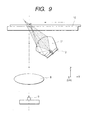
- Fig. 9 is a cross sectional view schematically showing the principal portion of an image reading apparatus in which an illumination apparatus according to any one of the first to fourth embodiments is used.
- the image reading apparatus shown in Fig. 9 uses multiple illumination units 11 arranged in the direction of line Lm (i.e. X-direction) to illuminate a reflective original 10 at high efficiency.
- the illumination units 11 positioned on a substrate 2 forms a uniform focal lines that do not have directivity with respect to the direction of straight line Lm on a reading line Lr of the reflective original 10, and the focal lines are synthesized smoothly.
- an efficient line illumination is realized.
- an image of the reflective original illuminated by the light flux emitted from the illumination units 11 is formed (or imaged) on a one-dimensional line sensor (a CCD) 9 by an imaging lens 8 serving as imaging means.
- the reflective original 10 is shifted in the direction perpendicular to the one-dimensional line sensor 9, so that image information of the reflective original 10 is read.
- Fig. 10 is a cross sectional view schematically showing the principal portion of an image reading apparatus in which an illumination apparatus according to any one of the first to fourth embodiments is used.
- the image reading apparatus shown in Fig. 10 uses a single illumination unit 11.
- the light flux emitted from the illumination unit 11 is deflected by an optical element 12 such as a Fresnel lens to the direction toward entrance pupil of an imaging lens 8 so as to be delivered to a one-dimensional line sensor (a CCD) 9, wherein the system functions as a Koehler illumination system.
- This light flux is first imaged in air after it has passed through an optical element 12. Then an image of a reflective original disposed near the focal line is formed (or imaged) on the one-dimensional line sensor (CCD) 9 by the imaging lens 8.
- the reflective original 10 is shifted in the direction perpendicular to the plane of the drawing sheet of Fig. 10, so that image information of the reflective original 10 is read.
- Fig. 11 is a cross sectional view schematically showing the principal portion of an image reading apparatus of a 1:2-scanning type in which an illumination apparatus according to any one of the first to fourth embodiments is used.
- an original 61 is illuminated by the light flux emitted from an illumination unit 11, and the light path of the light flux reflected from the original is bent by first, second and third reflecting mirrors 65, 66 and 67 within the body of the apparatus, so that an image is formed on a one-dimensional line sensor (a CCD) 69 by an imaging lens 68 serving as imaging means.
- the first, second and third reflecting mirrors 65, 66 and 67 are moved for scanning in the sub-scanning direction while scanning in the main-scanning direction is performed electrically so that image information of the original would be read.
- the shift amount of the second and third reflecting mirrors 66 and 67 are adapted to be half the shift amount of the first reflecting mirror 65, in order to maintain the distance between the original and the one-dimensional line sensor constant.
- Fig. 11 is a cross sectional view schematically showing the principal portion of an image reading apparatus having an integrated carriage in which an illumination apparatus according to any one of the first to fourth embodiments is used.
- an original 81 is illuminated by the light flux emitted from an illumination unit 11, and the light path of the light flux reflected from the original is bent by first, second and third reflecting mirrors 85, 86 and 87 within the carriage 91, so that an image is formed on a one-dimensional line sensor (a CCD) 90 by an imaging lens 89 serving as imaging means.
- Image information of the original 81 is read while the carriage 91 is moved in the direction of arrow C shown in Fig. 12 (i.e. the sub-scanning direction) by a sub-scanning motor (not shown).
- an optical element having a reflecting surface composed as a portion of the inner side of a curved surface and a light source are used with 1 to 1 relationship.
- the structure of the optical element can be simplified and the size of the optical element can be reduced, while uniform line illumination is realized.
- adjustment for making the line illumination uniform can be additionally performed at the time of assembling.
- a versatile optical element and an illumination apparatus having such an optical element can be realized only by adjusting the number and the degree of density of the illumination units in accordance with the size of an original and specifications of the apparatus.
- the reflecting surface could have a shape formed by rotating a hyperbola about a rotation axis including its focus (strictly speaking, rotating one branch of a hyperbola about a rotation axis including the focus within the curve of that branch).
- This is less preferred, because it does not concentrate the light as much as a parabola or an ellipse, and the reflected light is still divergent. Nevertheless, some improvement in illumination distribution is obtained.
- the shape (i.e. the eccentricity) of the hyperbola changes with angle of rotation, preferably so that the locus of the focus within the other branch is a straight line parallel to the reading line Lr (see Fig. 7).
- the straight line will be the other side of the light source from the reading line Lr (i.e. below the light source in Fig. 7), rather than on the same side of the light source as in the case of line Lp for the ellipse.
- the axis of rotation should pass through (or near) the focus of the curve. It should not be parallel to the axis of the curve. It may be perpendicular to the axis of the curve, and will normally be generally transverse to the axis of the curve, e.g. within 5° to 10° of perpendicular to the curve axis.
Abstract
An embodiment of the present invention efficiently
shapes a light flux emitted from a light source into a
linear shape, and provides an
optical element having high versatility that can be widely used irrespective of the original sizes and to provide an illumination apparatus having such an illumination apparatus. The optical element has a reflection surface (3a) in the form of an inner side of a curved surface that is formed by rotating a parabola about a rotation axis (Ls) including the focus of the parabola or a point near the focus of the parabola.
optical element having high versatility that can be widely used irrespective of the original sizes and to provide an illumination apparatus having such an illumination apparatus. The optical element has a reflection surface (3a) in the form of an inner side of a curved surface that is formed by rotating a parabola about a rotation axis (Ls) including the focus of the parabola or a point near the focus of the parabola.
Description
- The present invention relates to an optical element and an illumination apparatus having the same. More specifically, the present invention relates to an optical element or an illumination apparatus having an optical element in which a light flux emitted from light source means is shaped so that line illumination would be efficiently effected. The optical element and the illumination apparatus according to the present invention would be preferably used in an image reading apparatus that utilizes a one-dimensional line sensor.
- Recently, as an apparatus for providing a line illumination for an image reading apparatus, there have been proposed various illumination apparatus that uses a light source (a point source) composed of a semiconductor device and effectively converges a light flux emitted from the light source onto the surface of an original to be illuminated. The light source composed of a semiconductor device is adopted in view of its advantages that its power consumption and heat generation are little and it does not require any particular lighting device.
- In this type of illumination apparatus, multiple light sources composed of semiconductor devices are arranged in the direction parallel to the line direction of the one-dimensional line sensor, and light fluxes emitted from the multiple light sources are converged onto the surface of an original by means of a single elongated reflecting member (or an optical element). Such an illumination apparatus was proposed by Japanese Patent Application Laid-Open No. 11-52136.
- However, efficient light conversion is highly sensitive to manufacturing error, and therefore, a high accuracy in its shape and its maintenance is required. This causes the following problems.
- (1) Since the size of the reflecting member is large, the mold used for manufacturing the same becomes large and its cost is very high.
- (2) Since the size of the reflecting member is large, it would deform after detached from the mold due to residual stress applied during the molding.
- (3) The relative positional relationship between the light source and the reflecting member is sensitive, and therefore curvature cannot be corrected satisfactorily.
- (4) Since the reflecting member is designed in conformity with the size of the original, it lacks versatility.
-
- An embodiment of the invention seeks to provide an optical element and an illumination apparatus using the same that can efficiently shape a light flux emitted from a light source into a linear light flux and that can be generally used irrespective of the original size.
- According to a first aspect of the present invention, there is provided an optical element having a reflecting surface in the form of an inner side of a curved surface that is formed by rotating a parabola about a rotation axis including the focus of the parabola.
- In the optical element according to the first aspect of the invention, the curved surface may have a shape that is formed when the parabola is rotated about the rotation axis through the angular range of ±45° to ±90° from a reference position.
- In the optical element according to the first aspect of the invention, the optical element may have a member used for assembling that is provided on a surface other than the reflecting surface.
- In the optical element according to the first aspect of the invention, the optical member may have a transparent member provided in a part of a space to which the reflecting surface is opposed.
- According to a second aspect of the present invention, there is provided an illumination apparatus comprising one or more illumination units each of which includes the optical element according to the first aspect of the invention or one of its modifications described above and light source means having a light emission point disposed at one focal point of the optical element, wherein said illumination apparatus illuminates a surface to be illuminated with a light flux from the light emission point via the optical element.
- According to a third · aspect of the present invention, there is provided an optical element having a reflecting surface in the form of an inner side of a curved surface that is formed by rotating an ellipse about a rotation axis including one of the focuses of the ellipse while changing the shape of the ellipse depending on a rotation angle of the ellipse about said rotation axis.
- In the optical element according to the third aspect of the invention, the curved surface may have a shape in which the other focus of the ellipse for forming the curved surface is on a first virtual straight line.
- In the optical element according to the third aspect of the invention, the curved surface may have a shape that is formed when the ellipse is rotated about the rotation axis through the angular range of ±45° to ±90° from a reference position.
- In the optical element according to the third aspect of the invention, the optical element may have a member used for assembling that is provided on a surface other than the reflecting surface.
- In the optical element according to the third aspect of the present invention, the optical member may have a transparent member provided in a part of a space to which the reflecting surface is opposed.
- According to a fourth aspect of the invention there is provided an illumination apparatus comprising one or more illumination units each of which includes an optical element according to the third aspect of the present invention or one of its modifications described above and light source means having a light emission point disposed at one focal point of said optical element, wherein the illumination apparatus illuminates a surface to be illuminated with a light flux from the light emission point via the optical element.
- In the illumination apparatus according to the fourth aspect of the invention, the transparent member may have an exit end surface of a substantially concentric circular arc shape with a center positioned on the rotation axis.
- This illumination apparatus may be designed in such a way that the exit end surface of the transparent member does not have a curvature in the direction parallel to said rotation axis.
- Alternatively, this illumination apparatus may be designed in such a way that the exit end surface of the transparent member has a curvature in the direction parallel to the rotation axis, the curvature varying in such a way that the power gradually decreases as the position shifts away from the first virtual straight line of the focus, the shape of the curved surface is such that the trajectory of the synthesized focus position determine taking into account the curvature imparted to the exit end surface corresponds to a second virtual straight line.
- In the illumination apparatus described just above, with the curvature varying in such a way that the power gradually decreases as the position shifts away from the first virtual straight line of the focus, the image position of the light emission point may be on the first virtual straight line.
- In the illumination apparatus according to the fourth aspect of the present invention, the curved surface may image a light flux emitted from said light emission point to form a focal line in a one-dimensional direction.
- In this illumination apparatus or in the illumination apparatus according to the second or fourth aspect of the present invention, the illumination apparatus may have a multiple number of said illumination units, and the multiple illumination units are disposed on a first virtual straight line that is formed by the curved surface of the light emission point.
- According to a fifth aspect of the present invention, there is provided an image reading apparatus for reading image information using on of the last two illumination apparatus described just above, or one of the illumination apparatus according to the second and fourth aspects of the present invention and imaging means for imaging image information that is linearly illuminated by the illumination apparatus onto a one-dimensional line sensor.
-
- Fig. 1 is a perspective view schematically showing the principal portion of an illumination unit according to the first embodiment of the present invention.
- Fig. 2 is a cross sectional view taken at Y-Z plane in Fig. 1 (i.e. vertical cross sectional view).
- Fig. 3 is a cross sectional view taken at X-Y plane in Fig. 1 (i.e. horizontal cross sectional view).
- Fig. 4 is a drawing illustrating how a portion of a quadratic curve forms a reflecting surface.
- Fig. 5 is a perspective view schematically showing the principal portion of a second embodiment of the present invention.
- Fig. 6 is a drawing illustrating how a portion of an ellipse forms a reflecting surface.
- Fig. 7 is a cross sectional view taken at X-Z plane in Fig. 5 (i.e. a side view).
- Fig. 8 is a cross sectional view taken at Y-Z plane in Fig. 5 (i.e. a vertical cross sectional view).
- Fig. 9 is a cross sectional view schematically showing the principal portion of an image reading apparatus provided with an illumination apparatus embodying the present invention.
- Fig. 10 is a cross sectional view schematically showing the principal portion of an image reading apparatus provided with an illumination apparatus embodying the present invention.
- Fig. 11 is a cross sectional view schematically showing the principal portion of an image reading apparatus provided with an illumination apparatus embodying the present invention.
- Fig. 12 is a cross sectional view schematically showing the principal portion of an image reading apparatus provided with an illumination apparatus embodying the present invention.
- Fig. 13 is a cross sectional view schematically showing the principal portion of a third embodiment of the present invention.
- Fig. 14 is a cross sectional view schematically showing the principal portion of the third embodiment of the present invention.
- Fig. 15 is a cross sectional view schematically showing the principal portion of a fourth embodiment of the present invention.
- Fig. 16 is a cross sectional view schematically showing the principal portion of a modification according to the present invention.
-
- Fig. 1 is a perspective view showing the principal part of an illumination apparatus using an optical element embodying the present invention. Fig. 2 is a cross sectional view (a vertical cross section) taken at Y-Z plane in Fig. 1. Fig. 3 is a cross sectional view (a horizontal cross section) taken at X-Y plane in Fig. 1.
- In Fig. 1,
reference numeral 1 designates light source means composed of a light source (a point source) that is arranged in such a way that a light emission point (i.e. a chip) 1a is positioned at or in the vicinity of one of the focuses of the reflective curved surface that forms an optical element 3 (described later). Thelight source 1 is bonded on asubstrate 2 at a predetermined position. Thelight source 1 comprises a semiconductor device that emits light from alight emission point 1a upon application of a voltage. Generally, thelight source 1 is designed in such a way as to have such a light distribution characteristic in which the emitted light damps in a cosine pattern in the perpendicular direction (i.e. Z-direction) from thelight emission point 1a. However, only a little part of the emitted light is effectively used for illuminating the original in the line direction (i.e. X-direction). - The
optical element 3 is composed of a reflecting member having a curved surface shape for collecting a part of the light flux that would otherwise be ineffectively used. The reflectingmember 3 has areflective surface 3a that is a part of the inner side of a curved surface formed by rotating a parabola about a rotation axis Ls that intersects the focus of the parabola or a point in the vicinity of that focus. This curved surface has a surface shape that is formed when the parabola is rotated about the rotation axis through the angular range, from a reference position, of ±45° to ±90°. In this connection, theoptical element 3 and the constituents of the light source means 1 are parts of an illumination unit (i.e. an illumination apparatus) 11. - The reflecting
member 3 is made of a transparent medium such as a plastic or glass material. - On the non-reflective bottom surface that is different from the reflecting surface of the reflecting
member 3, there is integrally formedpositioning pins 4 serving as assembling members. Thesepins 4 are fitted intopositioning holes 2a that are formed on thesubstrate 2 in advance. In the structure shown in Fig. 1, aframe member 5 for attaching the reflectingmember 3 is provided and the positioning pins 4 are formed thereon in order for the assembling operation to be effected by a single step, but the reflectingmember 3 may be divided into two parts having the same shape. In that case, the cost required for a mold can be reduced. - In the plane of
substrate 2, a straight line Lm is defined as a line passing through thelight source 1 and parallel to a reading line (the X-direction), and a straight line Ls is defined as a line orthogonal to the line Lm. Under the fitted state, an arbitral plane including the straight line Ls (i.e. such a plane that would be formed when a horizontal plane including the line Ls is rotated about the straight line Ls as the rotation axis) intersects the reflectingmember 3 to form intersection lines La and Lb, which are parts of a quadratic curve L1, ... , or Ln (see Fig. 4). In connection with this, the focus F1 of the quadratic curve L1 is at the position of thelight source 1 or in the vicinity of thelight source 1 within the range of a manufacturing error. - The rotation axis Ls may be any line (for example, the rotation axis Ls1 shown by a broken line in Fig. 4) as long as it includes the focus F1 or a point in the vicinity of the focus F1. The optical element has the reflecting surface(s) 3a in the form of the inner side of a curved surface that is formed when the parabola is rotated about the rotation axis Ls. In other words, the reflecting
member 3 has a reflecting surface Rm that is formed above thesubstrate 2 by rotating a predetermined parabola L1 having the focus positioned at thelight source 1 about the straight line Ls as the rotation axis. - While in this embodiment, the reflecting surface Rm is formed by the rotation angle of 180° (180 degrees), the reflecting surface would be preferably formed by the rotation angle of 90° to 180° in view of its light distribution. A light flux emitted from the
light emission point 1a may be directed downward to the transparent substrate, and the reflecting surface Rm may be arranged in conformity with the arrangement of such a light flux. - Fig. 2 is a vertical cross sectional view showing the
substrate 2 under the state in which the reflectingmember 3 is fitted into thesubstrate 2, taken at the plane including the line Ls. The quadratic curve L1 is a parabola having the focus at the position of the light source. The quadratic curve L1 is composed of curves L11 illustrated by solid lines existing above thesubstrate 2 and a curve L12 illustrated by a broken line beneath thesubstrate 2. A divergent light flux emitted from thelight source 1 is reflected by the reflectingsurface 3a of the reflectingmember 3 so as to be converted into a parallel light flux, which is to be effectively used for illuminating the surface of an original (not shown). - Fig. 3 is a horizontal cross sectional view showing the
substrate 2 under the state in which the reflectingmember 3 is fitted into thesubstrate 2, taken at the plane including the line Ls. The quadratic curve L1 is a parabola having the focus at the position of the light source. The quadratic curve L1 is composed of curves L11 illustrated by solid lines existing above thesubstrate 2 and a curve L12 illustrated by a broken line beneath thesubstrate 2. A divergent light flux emitted from thelight source 1 is, in Fig. 3 also, reflected by the reflectingsurface 3a of the reflectingmember 3 so as to be converted into a parallel light flux. In other words, the light flux emitted from thelight emission point 1a would be focused at infinity. - In practice, this light flux is rarely delivered to the surface of the original (not shown). However, since every intermediate cross sectional shape between those shown in Fig. 2 and Fig. 3 converts, with its portion of reflecting
surfaces 3a, a portion of the light flux into a parallel light flux and emits it, line illumination that is uniform along the reading line direction is realized, so that even if a plurality ofillumination units 11 is arranged in the X-direction, the light fluxes emitted from the illumination apparatus can be mixed uniformly without ripple. - In order to preserve such uniformity, it is desirable that the angle of the sector through which the reflecting surface Rm is formed be equal to or more than 90 degrees. If the angle is less than 90 degrees the directivity of the light fluxes emergent from the reflecting surface Rm becomes too sharp, so that ripple in the illumination intensity (i.e. unevenness in illumination) would tend to occur at the overlapping portions of the illumination areas. This might invite deterioration of image quality of the image reading apparatus especially when a positional displacement in the up and down direction of an original occurs.
- As per the above, in this embodiment, each reflecting
surface 3a of the reflectingmember 3 is of a form of a curved surface that is formed by rotating a parabola about a rotation axis Ls that includes the focus of the parabola or a point in the vicinity of the focus. With this feature, a light flux traveling away from the reading line direction is collected or converged appropriately, so that uniform line illumination can be realized. In addition, effective line illumination can be realized by setting the number and density of theillumination units 11 having the light sources 1 (orlight emission points 1a) and theoptical elements 3 appropriately in accordance with the size of the original and the required light quantity. Furthermore, since each reflectingsurface 3a is formed to have a rotated parabola shape, the shape is not complex and the invention can be realized using the same shape that is symmetry with respect to the rotation axis Ls. - In this embodiment, the reflecting
surfaces 3a are formed as portions of the inner side of a curved surface that is formed by rotating a parabola as a quadratic curve about a rotation axis including its focus or a point in the vicinity of the focus, and two reflecting curved surfaces thus formed that are of the same shape and symmetrical with each other have been described in the foregoing. In practice, however, the two reflecting surfaces may be asymmetrical, or the illuminating directions for the two curved surfaces may be set independently from each other in accordance with the area to be illuminated. - It should be noted that the purpose of the reflecting curved surface is attained only if a reflected light flux is delivered to a predetermined area to be illuminated. Therefore, it would also be effective to form a microstructure on the reflecting surface to impart a diffusing property having a reflection directivity to the surface in order to reduce requirements for its manufacturing or assembling accuracy. Alternatively, the curved surface shape may be formed by approximation with a polyhedral shape that behaves in substantially the same manner as a curved surface.
- Fig. 5 is a perspective view showing the principal part of an illumination apparatus as a second embodiment of the present invention. Fig. 6 is a diagram illustrating how portions of an ellipse are used as reflecting surfaces. In Fig. 5, elements that are the same as those shown in Fig. 1 are designated with the same reference numerals.
- In this embodiment, a reflecting surface(s) 51b is formed as a portion(s) of the inner side of a curved surface that is formed by rotating an
ellipse 51 about a rotation axis Ls that includes one of the focuses of theellipse 51 or apoint 51a near the focus while changing the shape of theellipse 51 in accordance with rotational angle about the rotation axis Ls. - Specifically, when the shape of the curved surface is formed, the shape of the ellipse is varied in accordance with the rotational angle about the rotation axis Ls in such a way that the other focus of the ellipse or a
point 51c near the other focus is positioned on a virtual line that is parallel to an image reading line Lr. - The above-mentioned curved surfaces has a surface shape that is formed when the ellipse is rotated about the rotation axis Ls through the angular range, from a reference position, of ±45° to ±90°.
- Fig. 7 is a cross sectional side view taken at X-Z plane of Fig. 5. Fig. 7 illustrates the principle for defining the shape of the reflecting surface Rm of the reflecting
member 3. - In Fig. 7, reference sign GB designates a transparent medium (e.g. a plastic or glass) that is disposed in a space to which the reflecting surface Rm is opposed. The medium GB covers the
light source 1. The reflectingmember 3 is disposed on the medium GB. - In Fig. 5, there is illustrated a semiconductor light emitting device (i.e. the light source) 1 generally having a lens hood. The reflecting surface Rm whose line of intersection with a plane including the straight line Ls constitutes an ellipse having a focus at the
light emission point 1a is provided on a part of a lens hood portion of the semiconductorlight emitting device 1 having electrically conductive leads for wiring provided in advance. After theoptical element 3 is mounted on thesubstrate 2 with positioning pins (i.e. assembling members) formed on the bottom, the electrically conductive leads are soldered. - Fig.7 is a side view showing this state, wherein straight line Lr is a virtual line along which reading of an image is assumed to be performed. Here, a description will be made of how the shape of the reflecting surface(s) Rm is determined. When reading points p1, p2, p3, p4, ..., and pn on the image reading line Lr are arbitrary designated, the line of
intersection 3P of the plane Dm that includes point pn and the straight line Ls and the reflecting surface Rm of the reflectingmember 3 has one of the focuses at the position of thelight source 1. The other focus pn' (which focus pn' is determined taking into account the difference in media) is present on the straight line including thelight source 1 and the point pn, and the straight line Lp including points pn' (n=1, 2, 3, ...) is parallel to the reading line Lr. The reflecting surface Rm is so determined that all of the above conditions are met. - As per the above, the reflecting surface (curved surface) Rm images the light flux emitted from the
light emission point 1a to form a focal line in a one-dimensional direction. - With the above-described arrangement, a light flux emitted from the light source is reflected by the reflecting surfaces Rm so that a smooth focal line is formed in parallel with the reading line Lr. The intensity of this line illumination becomes low as the position changes from its center to the periphery. Therefore, a plurality of such line illumination structures are used in an overlapping manner to attain effective line illumination.
- In addition, in order to enhance efficiency of illumination, a light flux incident on a hatched
portion 13 in Fig. 7 is adapted to be reflected by a reflectingsurface 6, so that the light is efficiently used. For example, if the hatchedportion 13 is formed as a shape of paraboloid, the shape of the reflectingsurface 6 may be a fine cylindrical surface or a Fresnel reflective surface. - Fig. 8 is a cross sectional view taken at Y-Z plane of Fig. 5, which corresponds to an arbitrary cross section including the straight line Ls.
- In Fig. 8, a light flux emitted from the
light emission point 1a provided at one of the focuses F1 is reflected by the reflecting surface Rm of theoptical element 3 and then converged at the other focus F2. In connection with this, the light converging point F2 is arranged at a position on thelight source 1 side with respect to the reading line Lr, in order to enhance illumination efficiency. - In order for illumination with a practically usable width to be provided efficiently, the light
exit end surface 7 of the medium GB is designed to be a circular shape, a toric shape or a cylindrical shape. Therefore, the light flux emergent from the medium GB is substantially perpendicular to thatsurface 7. - The light
exit end surface 7 is designed to have a predetermined power in the direction of line Ls. Alternatively, the lightexit end surface 7 may be a flat plane. - The above-mentioned predetermined power is determined in such a way that a diverging light flux directly comes from the light source is converged outside the reading line Lr so as to realize a limited width of illumination on the reading line Lr and the light reflected by the reflecting surface Rm is converged inside the reading line so as to realize an illumination width substantially the same as said limited width on the reading line Lr.
- More specifically, if the power of the light exit end surface is so arranged that the power gradually decreases as the position shifts from P1 to Pn in Fig. 7, conjugate relationship between the points P1' to Pn' and the
light source 1a can be preserved. In addition, since the points P1' to Pn' are arranged on a straight line, it is possible to form a focal line with a high degree of uniformity. In other words, it is possible to form a focal line with a high degree of uniformity even for light fluxes that do not pass through the reflectingcurved surface 3. In this case, the surface shape of the reflectingcurved surface 3 should be changed in such a way that the synthetic focus position follows a linear trajectory, taking into account the above-mentioned power of the light exit end surface. In this case, it would be also effective to design the shape of the lightexit end surface 7 in such a way that it has a little diverging property in order to enhance the degree of uniformity of the illumination area. - When the light
exit end surface 7 is designed to be a cylindrical surface without said power being imparted, the shape of the reflectingcurved surface 3 would be obtained by cutting elliptic cylinder in a circular arc manner with the light source being the center. Therefore, its manufacturing process can be greatly simplified. While in the foregoing, various combinations have been described, the combination may freely be made, and it is apparent that they may be adopted separately or in combination without any problem. - In this embodiment, the reflecting
surfaces 3a are formed as portions of the inner surface that is formed by rotating an ellipse as a quadratic curve about a rotation axis including its focus or a point in the vicinity of the focus, and two reflecting curved surfaces thus formed that are of the same shape and symmetrical with each other have been described in the foregoing. In practice, however, the two reflecting surfaces may be asymmetrical, or the positions of the focuses of the two curved surfaces may be set independently from each other in accordance with the area to be illuminated, or the shape of one of the curved surfaces may be such a shape that has multiple focuses. - It should be noted that the purpose of the reflecting curved surface is attained only if a reflected light flux is delivered to a predetermined area to be illuminated. Therefore, it would also be effective to form a microstructure on the reflecting surface to impart a diffusing property having a reflection directivity to the surface in order to reduce requirements for its manufacturing or assembling accuracy. Alternatively, the curved surface shape may be formed by approximation with a polyhedral shape that behaves substantially the same as a curved surface.
- In the case of the illumination apparatus that uses
multiple illumination units 11 havingoptical elements 3 and thelight sources 1 to illuminate a surface to be illuminated (i.e. the surface of an original) with light fluxes from light emission points via the optical elements, theillumination units 11 should be arranged in parallel with the direction of the reading line Lr (i.e. X-direction). - Various light sources have been used in image reading apparatus such as facsimile machines or image scanners for illuminating originals. As such a light source, an LED has been attracting attention, since it is advantageous for its low energy consumption and its high efficiency.
- In most cases, manufacturers of image reading apparatus purchase such light sources from manufacturers of the light sources and use (i.e. assemble) them in image reading apparatus. In other words, the user manufacturer of the light sources use them in various apparatus, and the optimal form of the light sources varies depending on the apparatus in which they are used. Therefore, from the standpoint of the manufacturer of the light sources, it is efficient to manufacture light sources that are as versatile (or general) as possible.
- In the case of LED light sources for example, a ready-made LED provided with a dome-like resin cover (an LED having a dome-like lens) is well known.
- For example, Japanese Utility Model Application Laid-Open No. 6-44267 discloses assembling that type of LEDs in a line and adjusting them in the optical axis direction to reduce the degree of unevenness of light quantity.
- However, such a light source provided with a dome-like resin cover requires high accuracy in positional relationship between the dome-like lens (collector lens) and the light emission point. In addition, the conventional dome-like shape is not optimal for use in an apparatus for providing line illumination.
- In view of the above situation, a light source apparatus (i.e. an illumination system) using a combination of an optical element that is optimal for line illumination and a light source has been proposed. However, the shape of the optical element used in this light source apparatus is optimized for use in an individual type of the light source apparatus. Viewed from the standpoint of a manufacturer of light sources, a resin cover manufactured with the shape optimized for the above-mentioned apparatus has low versatility, since the optimal shape varies depending on its application. Therefore, the optimized shape suffers from a problem in its application.
- An embodiment of the present invention seeks to provide a light source apparatus and an illumination apparatus using the light source apparatus that uses a general light source such as an LED manufactured by a light source manufacturer without any modification, while illuminating a required illumination area efficiently and realizing sufficient accuracy required by users.
- Fig. 13 is a cross sectional view of the principal portion of an illumination apparatus as a third embodiment of the present invention. Fig. 14 is a cross sectional view of the principal portion, in which an
optical element 101 and alight source portion 102, which are separated in Fig. 13, are connected together. - In Figs. 13 and 14,
reference numeral 111 designates a light source device having theoptical element 101 and the light source portion (a light source) 102 composed of an LED having a dome-like lens. - The
light source portion 102 has alight emitting portion 102a, a ready-made transparent member (i.e. a dome-like lens) 102b having a light-collecting function on the light emission side of the light emitting portion. - The
optical element 101 is made of a material that is transparent to the light emitted from thelight emitting portion 102a. Theoptical element 101 has afitting portion 101a having a shape compliant with the shape of thelight emitting surface 102c of the ready-made transparent member, and alight emitting surface 101b that changes the state of the light flux that has entered theoptical element 101 from thefitting portion 101a to emit it. Here, the word "transparent" should be interpreted in relation to the principal wavelength of the light emitted from the light emitting portion, and it does not necessarily mean transparent to the visible light range. Furthermore, the word "transparent" means that absorption is low. In addition, a surface of each portion may have a diffusing property in order to reduce sensitivity in positional accuracy. - The ready-made
transparent member 102b of thelight source portion 102 is fitted into and secured to thefitting portion 101a of theoptical element 101 so that the light flux emitted from thelight emitting portion 102a would be delivered to a predetermined illumination area via thelight emitting surface 101b of the optical element. In other words, thefitting portion 101a and the ready-madetransparent member 102b are secured together after they are so aligned that illumination distribution in the above-mentioned predetermined illumination area is adjust to be in a predetermined range. - As described above, the
optical element 101 has a fitting portion into which the ready-madetransparent member 102b can be fitted. When they are fitted and secured together without a space therebetween, the state shown in Fig. 14 is realized. Since in this fitted and secured state, the accuracy of the position of thelight emitting portion 102a is determined by the accuracy of the position of thelight source portion 102, it is superior in productivity in the case in which the designed shape of theoptical element 101 is not sensitive to (i.e. easily influenced by) the position of thelight source portion 102. In addition, it is possible to reduce cost by virtue of its simple structure. - As per the above, in this embodiment the
fitting portion 101a into which the ready-madetransparent member 102b that is generally manufactured by a light source manufacturer can be fitted is provided on theoptical element 101 made of a material transparent to the light emitted from the light emitting portion, and theoptical element 101 and thelight source portion 102 are joined together. Thus, the user manufacturer can optimally use light sources while preserving versatility of the light sources supplied by light source manufacturers. - Fig. 15 is a cross sectional view of the principal portion of an illumination apparatus as a fourth embodiment of the present invention. In Fig. 13, the elements the same as those shown in Fig. 13 are designated with the same reference signs.
- This fourth embodiment differs from the above-described third embodiment in that a
space 105 is formed between afitting portion 101a of anoptical element 101 and a ready-madetransparent member 102b of alight source portion 102, and thespace 105 is filled with transparent adhesive so that theoptical element 101 and thelight source portion 102 are attached. The structure and the optical functions of the fourth embodiment other than the above are the same as those of the third embodiment, and therefore the same advantageous effects can be carried out in this fourth embodiment too. - When illumination efficiency of the light source apparatus (i.e. an illumination system) is increased, the typical degree of manufacturing precision of light sources generally available in the market does not meet the requirement for accuracy in the position of the optical element relative to the
light emitting portion 102a. - In view of this fact, in this embodiment, the size of the
fitting portion 101a is designed to be a little larger than the size of the ready-madetransparent member 102b of thelight source portion 102, and thespace 105 formed between them is filled with atransparent adhesive 103, so that thelight source portion 102 is shifted in thefitting portion 101a. Thus, the position adjustment such as an adjustment of the optical axis is effected, and then the adhesive 103 is cured so that theoptical element 101 and thelight source portion 102 are joined. In connection with this, the position adjustment may be carried out while observing outputs of multiplelight receiving sensors 104 disposed in the illumination area. Thelight receiving sensors 104 may be PIN photo diodes, and the adjustment may be performed while measuring symmetry in the light quantity distribution, or alternatively, the luminance distribution itself may be measured by means of a certain element such as a CCD to perform the position adjustment with a higher degree of accuracy. - The above-mentioned curing may be performed naturally, but use of a heat curing adhesive or a UV curing adhesive would be more desirable in order to increase productivity. In the example shown in Fig. 15, UV light is externally radiated for curing, a heating effect or light emission of the light source itself may serve as a heat source for provisional curing or a UV light source with its heat generation or light emission, if the type of the light source is suitable for those purposes.
- As per the above, in this embodiment a
space 105 is formed between thefitting portion 101a of theoptical element 101 and the ready-madetransparent member 102b of thelight source portion 102, and thespace 105 is filled with the adhesive 103. Thus, by the same token as the third embodiment, the user manufacturer can optimally use light sources while preserving versatility of the light sources supplied by light source manufacturers. - In this embodiment, if the
optical element 101 and the adhesive 103 have a refractive index substantially the same as that of the resin of the ready-made transparent member (or dome-like lens), the influence of refraction at the joining portion can be suppressed. This makes designing of the apparatus easy. In addition, it is also possible to enhance efficiency in taking out a light flux that would be otherwise totally reflected at the surface of the ready-madetransparent member 102b. - Furthermore, if the coefficient of thermal expansion of the
optical element 101, that of the ready-madetransparent member 102b and that of thetransparent adhesive 103 after cured are the same, distortion of their shapes caused by environmental changes during the light emission can be suppressed. Here, the transparent adhesive refers to an adhesive that does not positively absorb the light emitted from the light source. There is no problem if the transparent adhesive has a diffusing property after it is cured. Furthermore, this would be rather preferable, since this might reduce the sensitivity to accuracy in the position of the light source. (Modifications) - In the following, modifications of the
embodiments - As shown in Fig. 16, fitting and securing of the
light source portion 102 to theoptical element 101 may be performed by lightly pressing the ready-madetransparent member 102b of thelight source portion 102 into the fitting portion, which has a shape corresponding to the shape of thetransparent member 102b, to partially deform the optical element. - In the above-described third and fourth embodiments described above, the descriptions have been made in connection with such a light source portion that has an LED with a dome-like lens. However, the form of the light source portion is not limited to this, but light source portions having other various shapes such as a rectangular parallelepiped or a circular cylinder may also be used in a similar manner.
- The shape of the optical element is not limited to the dome-like shape indicated in the third and fourth embodiments, but the present invention is applicable to optical elements formed with
fitting portions 101a that have other shapes in accordance with light source devices used for various applications. - While various examples and embodiments of the present invention have been described, a person skilled in the art would understand that the concept and scope of the invention are not limited to the specific descriptions and drawings made in the specification but cover various modifications and changes.
- In the following, some mode in accordance with the third and fourth embodiments of the present invention will be mentioned.
- A light source apparatus having a light source portion and an optical element for causing a light flux from the light source portion to be incident on a predetermined illumination area, wherein the light source portion has a transparent member having a function of collecting light on the light emission side (or emergence side) of its light emitting portion, the optical element has a fitting portion having a shape corresponding to the shape of the light emergence surface of the transparent member and a light emergence surface which changes the state of the light flux from the fitting portion when the light flux is emitted from it, and the transparent member of the optical element is fitted and secured to the fitting portion of the optical element.
- The light source apparatus according to
mode 1, wherein the transparent member of the light source portion is fitted and secured to the fitting portion of the optical element by weak press fitting. - The light source apparatus according to
mode 1, wherein a space is formed between the fitting portion of the optical element and the transparent member of the light source portion and said space is filled with a transparent adhesive. - The light source apparatus according to
mode 1, wherein the fitting portion of the optical element and the transparent member of the light source portion are secured after they are positioned in such a way that the luminance distribution in said predetermined illumination area is in a predetermined range. - An illumination apparatus provided with one or more light source apparatus according to either one of the above-described
modes 1 to 4, to illuminate a surface to be illuminated. - An image reading apparatus that read image information using the illumination apparatus described in
mode 5 and imaging means for imaging the image information illuminated by the illumination apparatus onto a one-dimensional line sensor. - Fig. 9 is a cross sectional view schematically showing the principal portion of an image reading apparatus in which an illumination apparatus according to any one of the first to fourth embodiments is used. The image reading apparatus shown in Fig. 9 uses
multiple illumination units 11 arranged in the direction of line Lm (i.e. X-direction) to illuminate a reflective original 10 at high efficiency. - In the apparatus shown in Fig. 9, the
illumination units 11 positioned on asubstrate 2 forms a uniform focal lines that do not have directivity with respect to the direction of straight line Lm on a reading line Lr of the reflective original 10, and the focal lines are synthesized smoothly. Thus, an efficient line illumination is realized. - In the apparatus shown in Fig. 9, an image of the reflective original illuminated by the light flux emitted from the
illumination units 11 is formed (or imaged) on a one-dimensional line sensor (a CCD) 9 by animaging lens 8 serving as imaging means. The reflective original 10 is shifted in the direction perpendicular to the one-dimensional line sensor 9, so that image information of the reflective original 10 is read. - Fig. 10 is a cross sectional view schematically showing the principal portion of an image reading apparatus in which an illumination apparatus according to any one of the first to fourth embodiments is used. The image reading apparatus shown in Fig. 10 uses a
single illumination unit 11. - In the image reading apparatus shown in Fig. 9, the light flux emitted from the
illumination unit 11 is deflected by anoptical element 12 such as a Fresnel lens to the direction toward entrance pupil of animaging lens 8 so as to be delivered to a one-dimensional line sensor (a CCD) 9, wherein the system functions as a Koehler illumination system. This light flux is first imaged in air after it has passed through anoptical element 12. Then an image of a reflective original disposed near the focal line is formed (or imaged) on the one-dimensional line sensor (CCD) 9 by theimaging lens 8. The reflective original 10 is shifted in the direction perpendicular to the plane of the drawing sheet of Fig. 10, so that image information of the reflective original 10 is read. - Fig. 11 is a cross sectional view schematically showing the principal portion of an image reading apparatus of a 1:2-scanning type in which an illumination apparatus according to any one of the first to fourth embodiments is used.
- In the image reading apparatus shown in Fig. 11, an original 61 is illuminated by the light flux emitted from an
illumination unit 11, and the light path of the light flux reflected from the original is bent by first, second and third reflectingmirrors imaging lens 68 serving as imaging means. In this process, the first, second and third reflectingmirrors mirrors mirror 65, in order to maintain the distance between the original and the one-dimensional line sensor constant. - Fig. 11 is a cross sectional view schematically showing the principal portion of an image reading apparatus having an integrated carriage in which an illumination apparatus according to any one of the first to fourth embodiments is used.
- In the image reading apparatus shown in Fig. 12, an original 81 is illuminated by the light flux emitted from an
illumination unit 11, and the light path of the light flux reflected from the original is bent by first, second and third reflectingmirrors carriage 91, so that an image is formed on a one-dimensional line sensor (a CCD) 90 by animaging lens 89 serving as imaging means. Image information of the original 81 is read while thecarriage 91 is moved in the direction of arrow C shown in Fig. 12 (i.e. the sub-scanning direction) by a sub-scanning motor (not shown). - The above-described examples may be applied to various color image reading apparatus such as digital color copying machines and color image scanners.
- As has been described in the foregoing, in the embodiments, an optical element having a reflecting surface composed as a portion of the inner side of a curved surface and a light source are used with 1 to 1 relationship. With this structure, the structure of the optical element can be simplified and the size of the optical element can be reduced, while uniform line illumination is realized. In addition, adjustment for making the line illumination uniform can be additionally performed at the time of assembling. Thus, a versatile optical element and an illumination apparatus having such an optical element can be realized only by adjusting the number and the degree of density of the illumination units in accordance with the size of an original and specifications of the apparatus.
- As an alternative, the reflecting surface could have a shape formed by rotating a hyperbola about a rotation axis including its focus (strictly speaking, rotating one branch of a hyperbola about a rotation axis including the focus within the curve of that branch). This is less preferred, because it does not concentrate the light as much as a parabola or an ellipse, and the reflected light is still divergent. Nevertheless, some improvement in illumination distribution is obtained. As in the case of an ellipse, it is preferred that the shape (i.e. the eccentricity) of the hyperbola changes with angle of rotation, preferably so that the locus of the focus within the other branch is a straight line parallel to the reading line Lr (see Fig. 7). However, in this case the straight line will be the other side of the light source from the reading line Lr (i.e. below the light source in Fig. 7), rather than on the same side of the light source as in the case of line Lp for the ellipse.
- The axis of rotation should pass through (or near) the focus of the curve. It should not be parallel to the axis of the curve. It may be perpendicular to the axis of the curve, and will normally be generally transverse to the axis of the curve, e.g. within 5° to 10° of perpendicular to the curve axis.
Claims (22)
- An optical element having a reflecting surface in the form of an inner side of a curved surface that is formed by rotating a parabola about a rotation axis including the focus of the parabola.
- An optical element according to claim 1, wherein said curved surface has a shape that is formed when the parabola is rotated about said rotation axis through the angular range of ±45° to ±90° from a reference position.
- An optical element according to claim 1 or 2, wherein said optical element has a member used for assembling that is provided on a surface other than said reflecting surface.
- An optical element according to any one of claims 1 to 3, wherein said optical member has a transparent member provided in a part of a space to which said reflecting surface is opposed.
- An illumination apparatus comprising one or more illumination units each of which includes an optical element according to any one of claims 1 to 4 and light source means having a light emission point disposed at one focal point of said optical element, wherein said illumination apparatus illuminates a surface to be illuminated with a light flux from said light emission point via said optical element.
- An optical element having a reflecting surface in the form of an inner side of a curved surface that is formed by rotating an ellipse about a rotation axis including one of the focuses of the ellipse while changing the shape of the ellipse depending on a rotation angle of the ellipse about said rotation axis.
- An optical element according to claim 6, wherein said curved surface has a shape in which the other focus of the ellipse for forming said curved surface is on a first virtual straight line.
- An optical element according to claim 6 or 7, wherein said curved surface has a shape that is formed when the ellipse is rotated about said rotation axis through the angular range of ±45° to ±90° from a reference position.
- An optical element according to any one of claims 6 to 8, wherein said optical element has a member used for assembling that is provided on a surface other than said reflecting surface.
- An optical element according to any one of claims 6 to 9, wherein said optical member has a transparent member provided in a part of a space to which said reflecting surface is opposed.
- An illumination apparatus comprising one or more illumination units each of which includes an optical element according to any one of claims 6 to 10 and light source means having a light emission point disposed at one focal point of said optical element, wherein said illumination apparatus illuminates a surface to be illuminated with a light flux from said light emission point via said optical element.
- An illumination apparatus according to claim 11, wherein said transparent member has an exit end surface of a substantially concentric circular arc shape with a center positioned on said rotation axis.
- An illumination apparatus according to claim 12, wherein the exit end surface of said transparent member does not have a curvature in the direction parallel to said rotation axis.
- An illumination apparatus according to claim 11 or 12, wherein the exit end surface of said transparent member has a curvature in the direction parallel to said rotation axis, the curvature varying in such a way that the power gradually decreases as the position shifts away from said first virtual straight line of the focus, the shape of said curved surface is such that the trajectory of the synthesized focus position determine taking into account the curvature imparted to said exit end surface corresponds to a second virtual straight line.
- An illumination apparatus according to claim 14, wherein with said curvature varying in such a way that the power gradually decreases as the position shifts away from said first virtual straight line of the focus, the image position of said light emission point is on the first virtual straight line.
- An illumination apparatus according to claim 11, wherein said curved surface images a light flux emitted from said light emission point to form a focal line in a one-dimensional direction.
- An illumination apparatus according to claim 5, 11 or 16, wherein said illumination apparatus has a multiple number of said illumination units, and said multiple illumination units are disposed on a first virtual straight line that is formed by said curved surface of said light emission point.
- An image reading apparatus for reading image formation using an illumination apparatus according to claims 5, 11, 16 or 17 and imaging means for imaging image information that is linearly illuminated by said illumination apparatus onto a one-dimensional line sensor.
- An optical element having a reflecting surface having the shape formed by rotating a curve having at least one focus about an axis of rotation passing through the focus, or one of the foci, the axis of rotation not being parallel to the axis of the curve.
- An optical element according to claim 19 in which the eccentricity of the curve varies with its angle of rotation about the axis of rotation.
- An optical element according to claim 20 in which the curve has, or is associated with, first and second foci, the axis of rotation passes through the first focus, and the eccentricity varies such that the locus of the second focus, as the curve rotates about the axis of rotation, is substantially a straight line.
- An illumination unit comprising an optical element according to any one of claims 19 to 21 and a light source substantially at the focus through which the axis of rotation passes.
Applications Claiming Priority (4)
| Application Number | Priority Date | Filing Date | Title |
|---|---|---|---|
| JP2002152210 | 2002-05-27 | ||
| JP2002152210A JP2003344958A (en) | 2002-05-27 | 2002-05-27 | Optical element and illuminating device having the same |
| JP2002192064A JP2004039334A (en) | 2002-07-01 | 2002-07-01 | Light source device, and lighting system using it |
| JP2002192064 | 2002-07-01 |
Publications (1)
| Publication Number | Publication Date |
|---|---|
| EP1367413A1 true EP1367413A1 (en) | 2003-12-03 |
Family
ID=29422452
Family Applications (1)
| Application Number | Title | Priority Date | Filing Date |
|---|---|---|---|
| EP03253313A Withdrawn EP1367413A1 (en) | 2002-05-27 | 2003-05-27 | Reflector and linear illumination device |
Country Status (3)
| Country | Link |
|---|---|
| US (1) | US7336403B2 (en) |
| EP (1) | EP1367413A1 (en) |
| CN (1) | CN1229654C (en) |
Cited By (3)
| Publication number | Priority date | Publication date | Assignee | Title |
|---|---|---|---|---|
| US8227821B2 (en) | 2004-09-22 | 2012-07-24 | Osram Opto Semiconductors Gmbh | Housing for an optoelectronic component, optoelectronic component and method for the production of an optoelectronic component |
| US8446004B2 (en) | 2004-06-04 | 2013-05-21 | Cree, Inc. | Power light emitting die package with reflecting lens and the method of making the same |
| DK201370715A1 (en) * | 2013-11-21 | 2015-06-01 | Martin Professional Aps | Illumination system comprising an optical light mixing rod |
Families Citing this family (7)
| Publication number | Priority date | Publication date | Assignee | Title |
|---|---|---|---|---|
| US20060152805A1 (en) * | 2003-06-25 | 2006-07-13 | Makoto Ikeda | Light guide and line illuminator |
| TWI465147B (en) * | 2006-07-31 | 2014-12-11 | 3M Innovative Properties Co | Led source with hollow collection lens |
| WO2011096411A1 (en) * | 2010-02-05 | 2011-08-11 | 株式会社 東芝 | Illumination device and image-reading device provided with illumination device |
| CN106218456A (en) * | 2016-09-13 | 2016-12-14 | 吴耀南 | A kind of portable child seat |
| CN106274568A (en) * | 2016-09-13 | 2017-01-04 | 吴耀南 | A kind of foldable child safety seat |
| CN108429869B (en) * | 2018-03-22 | 2024-02-06 | 威海华菱光电股份有限公司 | Image reading apparatus |
| CN115824047B (en) * | 2022-12-06 | 2023-12-08 | 国网四川省电力公司映秀湾水力发电总厂 | Alignment method for geometrical center position of unit component |
Citations (5)
| Publication number | Priority date | Publication date | Assignee | Title |
|---|---|---|---|---|
| WO1998020365A1 (en) * | 1996-11-05 | 1998-05-14 | Corrosion Consultants, Inc. | Ultraviolet light illumination and viewing system and method for fluorescent dye leak detection |
| US5764783A (en) * | 1996-01-16 | 1998-06-09 | Technology Licensing Company | Variable beamwidth transducer |
| US6072171A (en) * | 1995-08-24 | 2000-06-06 | Matsushita Electric Industrial Co., Ltd. | Linear illumination device |
| US20020006039A1 (en) * | 2000-07-14 | 2002-01-17 | Kyoto Denkiki Co., Ltd. | Linear lighting system |
| US6355946B1 (en) * | 1998-12-16 | 2002-03-12 | Rohm Co., Ltd. | Semiconductor device with reflector |
Family Cites Families (18)
| Publication number | Priority date | Publication date | Assignee | Title |
|---|---|---|---|---|
| US3982824A (en) * | 1971-12-01 | 1976-09-28 | Raytheon Company | Catoptric lens arrangement |
| US3871751A (en) * | 1973-07-02 | 1975-03-18 | Raytheon Co | Catoptric lens arrangement |
| US4751427A (en) * | 1984-03-12 | 1988-06-14 | Planar Systems, Inc. | Thin-film electroluminescent device |
| US4794427A (en) * | 1986-05-15 | 1988-12-27 | Canon Kabushiki Kaisha | Image scanning apparatus |
| JPS6314136A (en) * | 1986-07-07 | 1988-01-21 | Canon Inc | Reader/printer for microfilm |
| US5037191A (en) * | 1989-12-21 | 1991-08-06 | Cheng Dah Y | Orthogonal parabolic reflector systems |
| US5235470A (en) * | 1989-12-21 | 1993-08-10 | Cheng Dah Y | Orthogonal parabolic reflector systems |
| US5287147A (en) * | 1991-01-25 | 1994-02-15 | Canon Kabushiki Kaisha | Original scanning apparatus with fixed light source |
| JPH0644267A (en) | 1992-07-27 | 1994-02-18 | Tokyo Electric Co Ltd | Article sales data processor |
| US5659409A (en) * | 1992-10-09 | 1997-08-19 | Ag Technology Co., Ltd. | Light source apparatus using a cone-like material and an applied apparatus thereof |
| US5475571A (en) * | 1994-03-30 | 1995-12-12 | Ford Motor Company | Ring Light collector |
| JP3256409B2 (en) * | 1995-04-28 | 2002-02-12 | キヤノン株式会社 | Document illumination device |
| JP3453492B2 (en) * | 1997-05-13 | 2003-10-06 | キヤノン株式会社 | Image forming apparatus and printer head |
| JP3936438B2 (en) | 1997-07-31 | 2007-06-27 | ローム株式会社 | Image reading device |
| US6259082B1 (en) * | 1997-07-31 | 2001-07-10 | Rohm Co., Ltd. | Image reading apparatus |
| US6123436A (en) * | 1997-08-05 | 2000-09-26 | Vari-Lite, Inc. | Optical device for modifying the angular and spatial distribution of illuminating energy |
| DE60037427T2 (en) | 1999-07-21 | 2009-02-05 | Chi Mei Optoelectronics Corp. | ILLUMINATION DEVICE |
| US6801298B2 (en) * | 2002-07-25 | 2004-10-05 | Intel Corporation | Light condenser |
-
2003
- 2003-05-16 US US10/439,239 patent/US7336403B2/en not_active Expired - Fee Related
- 2003-05-26 CN CN03138421.8A patent/CN1229654C/en not_active Expired - Fee Related
- 2003-05-27 EP EP03253313A patent/EP1367413A1/en not_active Withdrawn
Patent Citations (5)
| Publication number | Priority date | Publication date | Assignee | Title |
|---|---|---|---|---|
| US6072171A (en) * | 1995-08-24 | 2000-06-06 | Matsushita Electric Industrial Co., Ltd. | Linear illumination device |
| US5764783A (en) * | 1996-01-16 | 1998-06-09 | Technology Licensing Company | Variable beamwidth transducer |
| WO1998020365A1 (en) * | 1996-11-05 | 1998-05-14 | Corrosion Consultants, Inc. | Ultraviolet light illumination and viewing system and method for fluorescent dye leak detection |
| US6355946B1 (en) * | 1998-12-16 | 2002-03-12 | Rohm Co., Ltd. | Semiconductor device with reflector |
| US20020006039A1 (en) * | 2000-07-14 | 2002-01-17 | Kyoto Denkiki Co., Ltd. | Linear lighting system |
Cited By (8)
| Publication number | Priority date | Publication date | Assignee | Title |
|---|---|---|---|---|
| US8446004B2 (en) | 2004-06-04 | 2013-05-21 | Cree, Inc. | Power light emitting die package with reflecting lens and the method of making the same |
| US8932886B2 (en) | 2004-06-04 | 2015-01-13 | Cree, Inc. | Power light emitting die package with reflecting lens and the method of making the same |
| US8227821B2 (en) | 2004-09-22 | 2012-07-24 | Osram Opto Semiconductors Gmbh | Housing for an optoelectronic component, optoelectronic component and method for the production of an optoelectronic component |
| EP1792351B1 (en) * | 2004-09-22 | 2016-07-27 | OSRAM Opto Semiconductors GmbH | Housing for an optoelectronic component, optoelectronic component and method for the production of an optoelectronic component |
| DK201370715A1 (en) * | 2013-11-21 | 2015-06-01 | Martin Professional Aps | Illumination system comprising an optical light mixing rod |
| DK178386B1 (en) * | 2013-11-21 | 2016-01-25 | Martin Professional Aps | Illumination system comprising an optical light mixing rod |
| US9523806B2 (en) | 2013-11-21 | 2016-12-20 | Martin Professional Aps | Illumination system comprising an optical light mixing rod |
| US9612380B2 (en) | 2013-11-21 | 2017-04-04 | Martin Professional Aps | Illumination system comprising an optical light mixing rod and a pressure mechanism to apply a pressure force to the optical light mixing rod and to press an entrance surface and emitting window together |
Also Published As
| Publication number | Publication date |
|---|---|
| US7336403B2 (en) | 2008-02-26 |
| CN1469137A (en) | 2004-01-21 |
| US20030218811A1 (en) | 2003-11-27 |
| CN1229654C (en) | 2005-11-30 |
Similar Documents
| Publication | Publication Date | Title |
|---|---|---|
| US7085023B2 (en) | Image-reading apparatus | |
| US7431480B2 (en) | Optical element, compound optical element, and illuminating apparatus | |
| JP5654137B2 (en) | Illumination unit and image reading apparatus using the same | |
| US7953312B2 (en) | Light guiding member and bifurcated linear light source apparatus | |
| US9383501B2 (en) | Scanner module and image scanning apparatus employing the same | |
| JP5755753B2 (en) | Illumination unit and image reading apparatus using the same | |
| JPH09186824A (en) | Image reader | |
| US7336403B2 (en) | Optical element and illumination apparatus having same | |
| JP2001238048A (en) | Image reader and light guiding member used for the same | |
| JP2009053316A (en) | Lighting system, document reading apparatus, image reading device, image forming apparatus, and image transmitting/receiving device | |
| JP5018748B2 (en) | Contact image sensor | |
| US6160250A (en) | Integrated optical imaging assembly | |
| US7529445B2 (en) | Light guide and line illuminator | |
| JP5012790B2 (en) | Illumination device and image reading device using the same | |
| JP2010109652A (en) | Lighting equipment and image reader | |
| WO2005001529A1 (en) | Light guide and line illuminator | |
| JPH08172512A (en) | Lighting image-forming composite module and original reader using it | |
| JP2004039334A (en) | Light source device, and lighting system using it | |
| JP2003344958A (en) | Optical element and illuminating device having the same | |
| US7440151B2 (en) | Image reading apparatus | |
| JP2785758B2 (en) | Linear light source | |
| US7477424B2 (en) | Apparatus having a light source for a transparent sheet of a scanner | |
| JP5239232B2 (en) | Image reading apparatus and image forming apparatus | |
| JP2012059493A (en) | Light source device | |
| JP2000349971A (en) | Image reader and light guiding member used therefor |
Legal Events
| Date | Code | Title | Description |
|---|---|---|---|
| PUAI | Public reference made under article 153(3) epc to a published international application that has entered the european phase |
Free format text: ORIGINAL CODE: 0009012 |
|
| AK | Designated contracting states |
Kind code of ref document: A1 Designated state(s): AT BE BG CH CY CZ DE DK EE ES FI FR GB GR HU IE IT LI LU MC NL PT RO SE SI SK TR |
|
| AX | Request for extension of the european patent |
Extension state: AL LT LV MK |
|
| 17P | Request for examination filed |
Effective date: 20040426 |
|
| 17Q | First examination report despatched |
Effective date: 20040526 |
|
| AKX | Designation fees paid |
Designated state(s): DE FR GB IT NL SE |
|
| STAA | Information on the status of an ep patent application or granted ep patent |
Free format text: STATUS: THE APPLICATION HAS BEEN WITHDRAWN |
|
| 18W | Application withdrawn |
Effective date: 20060215 |