EP1174527A1 - Atomic layer deposition (ALD) film deposition equipment and cleaning method - Google Patents
Atomic layer deposition (ALD) film deposition equipment and cleaning method Download PDFInfo
- Publication number
- EP1174527A1 EP1174527A1 EP01304414A EP01304414A EP1174527A1 EP 1174527 A1 EP1174527 A1 EP 1174527A1 EP 01304414 A EP01304414 A EP 01304414A EP 01304414 A EP01304414 A EP 01304414A EP 1174527 A1 EP1174527 A1 EP 1174527A1
- Authority
- EP
- European Patent Office
- Prior art keywords
- gas
- reaction gas
- reactor
- cleaning
- thin film
- Prior art date
- Legal status (The legal status is an assumption and is not a legal conclusion. Google has not performed a legal analysis and makes no representation as to the accuracy of the status listed.)
- Withdrawn
Links
Images


Classifications
-
- H—ELECTRICITY
- H01—ELECTRIC ELEMENTS
- H01L—SEMICONDUCTOR DEVICES NOT COVERED BY CLASS H10
- H01L21/00—Processes or apparatus adapted for the manufacture or treatment of semiconductor or solid state devices or of parts thereof
- H01L21/02—Manufacture or treatment of semiconductor devices or of parts thereof
- H01L21/04—Manufacture or treatment of semiconductor devices or of parts thereof the devices having at least one potential-jump barrier or surface barrier, e.g. PN junction, depletion layer or carrier concentration layer
- H01L21/18—Manufacture or treatment of semiconductor devices or of parts thereof the devices having at least one potential-jump barrier or surface barrier, e.g. PN junction, depletion layer or carrier concentration layer the devices having semiconductor bodies comprising elements of Group IV of the Periodic System or AIIIBV compounds with or without impurities, e.g. doping materials
- H01L21/20—Deposition of semiconductor materials on a substrate, e.g. epitaxial growth solid phase epitaxy
-
- C—CHEMISTRY; METALLURGY
- C23—COATING METALLIC MATERIAL; COATING MATERIAL WITH METALLIC MATERIAL; CHEMICAL SURFACE TREATMENT; DIFFUSION TREATMENT OF METALLIC MATERIAL; COATING BY VACUUM EVAPORATION, BY SPUTTERING, BY ION IMPLANTATION OR BY CHEMICAL VAPOUR DEPOSITION, IN GENERAL; INHIBITING CORROSION OF METALLIC MATERIAL OR INCRUSTATION IN GENERAL
- C23C—COATING METALLIC MATERIAL; COATING MATERIAL WITH METALLIC MATERIAL; SURFACE TREATMENT OF METALLIC MATERIAL BY DIFFUSION INTO THE SURFACE, BY CHEMICAL CONVERSION OR SUBSTITUTION; COATING BY VACUUM EVAPORATION, BY SPUTTERING, BY ION IMPLANTATION OR BY CHEMICAL VAPOUR DEPOSITION, IN GENERAL
- C23C16/00—Chemical coating by decomposition of gaseous compounds, without leaving reaction products of surface material in the coating, i.e. chemical vapour deposition [CVD] processes
- C23C16/44—Chemical coating by decomposition of gaseous compounds, without leaving reaction products of surface material in the coating, i.e. chemical vapour deposition [CVD] processes characterised by the method of coating
- C23C16/455—Chemical coating by decomposition of gaseous compounds, without leaving reaction products of surface material in the coating, i.e. chemical vapour deposition [CVD] processes characterised by the method of coating characterised by the method used for introducing gases into reaction chamber or for modifying gas flows in reaction chamber
- C23C16/45563—Gas nozzles
- C23C16/45565—Shower nozzles
-
- C—CHEMISTRY; METALLURGY
- C23—COATING METALLIC MATERIAL; COATING MATERIAL WITH METALLIC MATERIAL; CHEMICAL SURFACE TREATMENT; DIFFUSION TREATMENT OF METALLIC MATERIAL; COATING BY VACUUM EVAPORATION, BY SPUTTERING, BY ION IMPLANTATION OR BY CHEMICAL VAPOUR DEPOSITION, IN GENERAL; INHIBITING CORROSION OF METALLIC MATERIAL OR INCRUSTATION IN GENERAL
- C23C—COATING METALLIC MATERIAL; COATING MATERIAL WITH METALLIC MATERIAL; SURFACE TREATMENT OF METALLIC MATERIAL BY DIFFUSION INTO THE SURFACE, BY CHEMICAL CONVERSION OR SUBSTITUTION; COATING BY VACUUM EVAPORATION, BY SPUTTERING, BY ION IMPLANTATION OR BY CHEMICAL VAPOUR DEPOSITION, IN GENERAL
- C23C16/00—Chemical coating by decomposition of gaseous compounds, without leaving reaction products of surface material in the coating, i.e. chemical vapour deposition [CVD] processes
- C23C16/44—Chemical coating by decomposition of gaseous compounds, without leaving reaction products of surface material in the coating, i.e. chemical vapour deposition [CVD] processes characterised by the method of coating
- C23C16/4401—Means for minimising impurities, e.g. dust, moisture or residual gas, in the reaction chamber
- C23C16/4405—Cleaning of reactor or parts inside the reactor by using reactive gases
-
- C—CHEMISTRY; METALLURGY
- C23—COATING METALLIC MATERIAL; COATING MATERIAL WITH METALLIC MATERIAL; CHEMICAL SURFACE TREATMENT; DIFFUSION TREATMENT OF METALLIC MATERIAL; COATING BY VACUUM EVAPORATION, BY SPUTTERING, BY ION IMPLANTATION OR BY CHEMICAL VAPOUR DEPOSITION, IN GENERAL; INHIBITING CORROSION OF METALLIC MATERIAL OR INCRUSTATION IN GENERAL
- C23C—COATING METALLIC MATERIAL; COATING MATERIAL WITH METALLIC MATERIAL; SURFACE TREATMENT OF METALLIC MATERIAL BY DIFFUSION INTO THE SURFACE, BY CHEMICAL CONVERSION OR SUBSTITUTION; COATING BY VACUUM EVAPORATION, BY SPUTTERING, BY ION IMPLANTATION OR BY CHEMICAL VAPOUR DEPOSITION, IN GENERAL
- C23C16/00—Chemical coating by decomposition of gaseous compounds, without leaving reaction products of surface material in the coating, i.e. chemical vapour deposition [CVD] processes
- C23C16/44—Chemical coating by decomposition of gaseous compounds, without leaving reaction products of surface material in the coating, i.e. chemical vapour deposition [CVD] processes characterised by the method of coating
- C23C16/455—Chemical coating by decomposition of gaseous compounds, without leaving reaction products of surface material in the coating, i.e. chemical vapour deposition [CVD] processes characterised by the method of coating characterised by the method used for introducing gases into reaction chamber or for modifying gas flows in reaction chamber
- C23C16/45519—Inert gas curtains
-
- C—CHEMISTRY; METALLURGY
- C23—COATING METALLIC MATERIAL; COATING MATERIAL WITH METALLIC MATERIAL; CHEMICAL SURFACE TREATMENT; DIFFUSION TREATMENT OF METALLIC MATERIAL; COATING BY VACUUM EVAPORATION, BY SPUTTERING, BY ION IMPLANTATION OR BY CHEMICAL VAPOUR DEPOSITION, IN GENERAL; INHIBITING CORROSION OF METALLIC MATERIAL OR INCRUSTATION IN GENERAL
- C23C—COATING METALLIC MATERIAL; COATING MATERIAL WITH METALLIC MATERIAL; SURFACE TREATMENT OF METALLIC MATERIAL BY DIFFUSION INTO THE SURFACE, BY CHEMICAL CONVERSION OR SUBSTITUTION; COATING BY VACUUM EVAPORATION, BY SPUTTERING, BY ION IMPLANTATION OR BY CHEMICAL VAPOUR DEPOSITION, IN GENERAL
- C23C16/00—Chemical coating by decomposition of gaseous compounds, without leaving reaction products of surface material in the coating, i.e. chemical vapour deposition [CVD] processes
- C23C16/44—Chemical coating by decomposition of gaseous compounds, without leaving reaction products of surface material in the coating, i.e. chemical vapour deposition [CVD] processes characterised by the method of coating
- C23C16/455—Chemical coating by decomposition of gaseous compounds, without leaving reaction products of surface material in the coating, i.e. chemical vapour deposition [CVD] processes characterised by the method of coating characterised by the method used for introducing gases into reaction chamber or for modifying gas flows in reaction chamber
- C23C16/45523—Pulsed gas flow or change of composition over time
- C23C16/45525—Atomic layer deposition [ALD]
- C23C16/45544—Atomic layer deposition [ALD] characterized by the apparatus
-
- C—CHEMISTRY; METALLURGY
- C23—COATING METALLIC MATERIAL; COATING MATERIAL WITH METALLIC MATERIAL; CHEMICAL SURFACE TREATMENT; DIFFUSION TREATMENT OF METALLIC MATERIAL; COATING BY VACUUM EVAPORATION, BY SPUTTERING, BY ION IMPLANTATION OR BY CHEMICAL VAPOUR DEPOSITION, IN GENERAL; INHIBITING CORROSION OF METALLIC MATERIAL OR INCRUSTATION IN GENERAL
- C23C—COATING METALLIC MATERIAL; COATING MATERIAL WITH METALLIC MATERIAL; SURFACE TREATMENT OF METALLIC MATERIAL BY DIFFUSION INTO THE SURFACE, BY CHEMICAL CONVERSION OR SUBSTITUTION; COATING BY VACUUM EVAPORATION, BY SPUTTERING, BY ION IMPLANTATION OR BY CHEMICAL VAPOUR DEPOSITION, IN GENERAL
- C23C16/00—Chemical coating by decomposition of gaseous compounds, without leaving reaction products of surface material in the coating, i.e. chemical vapour deposition [CVD] processes
- C23C16/44—Chemical coating by decomposition of gaseous compounds, without leaving reaction products of surface material in the coating, i.e. chemical vapour deposition [CVD] processes characterised by the method of coating
- C23C16/455—Chemical coating by decomposition of gaseous compounds, without leaving reaction products of surface material in the coating, i.e. chemical vapour deposition [CVD] processes characterised by the method of coating characterised by the method used for introducing gases into reaction chamber or for modifying gas flows in reaction chamber
- C23C16/45561—Gas plumbing upstream of the reaction chamber
-
- Y—GENERAL TAGGING OF NEW TECHNOLOGICAL DEVELOPMENTS; GENERAL TAGGING OF CROSS-SECTIONAL TECHNOLOGIES SPANNING OVER SEVERAL SECTIONS OF THE IPC; TECHNICAL SUBJECTS COVERED BY FORMER USPC CROSS-REFERENCE ART COLLECTIONS [XRACs] AND DIGESTS
- Y10—TECHNICAL SUBJECTS COVERED BY FORMER USPC
- Y10S—TECHNICAL SUBJECTS COVERED BY FORMER USPC CROSS-REFERENCE ART COLLECTIONS [XRACs] AND DIGESTS
- Y10S134/00—Cleaning and liquid contact with solids
- Y10S134/902—Semiconductor wafer
-
- Y—GENERAL TAGGING OF NEW TECHNOLOGICAL DEVELOPMENTS; GENERAL TAGGING OF CROSS-SECTIONAL TECHNOLOGIES SPANNING OVER SEVERAL SECTIONS OF THE IPC; TECHNICAL SUBJECTS COVERED BY FORMER USPC CROSS-REFERENCE ART COLLECTIONS [XRACs] AND DIGESTS
- Y10—TECHNICAL SUBJECTS COVERED BY FORMER USPC
- Y10S—TECHNICAL SUBJECTS COVERED BY FORMER USPC CROSS-REFERENCE ART COLLECTIONS [XRACs] AND DIGESTS
- Y10S438/00—Semiconductor device manufacturing: process
- Y10S438/905—Cleaning of reaction chamber
Definitions
- the present invention relates to atomic layer deposition (ALD) thin film deposition equipment, and more particularly, to ALD thin film deposition equipment employing a cleaning apparatus and a cleaning method.
- ALD atomic layer deposition
- Thin film deposition equipment forms a predetermined thin film on a wafer by supplying reaction gases to the wafer received within a reactor.
- This thin film deposition equipment includes chemical vapor deposition (CVD) thin film deposition equipment, atomic layer epitaxy (ALE) thin film deposition equipment, and others, and has been applied to various fields for manufacturing semiconductor devices.
- CVD chemical vapor deposition
- ALE atomic layer epitaxy
- a thin film is deposited not only on a wafer by an introduced reaction gas, but a thin film or process byproduct can also be deposited on the inner wall or component of a reactor, or on holes through which reaction gases are sprayed.
- a cleaning apparatus and method of effectively removing a thin film or a process byproduct deposited on the inner wall, components or holes of a reactor is required to effectively remove a thin film or a process byproduct deposited on the inner wall, components or holes of a reactor.
- An objective of the present invention is to provide an atomic layer deposition (ALD) thin film deposition equipment having a cleaning apparatus, and a cleaning method thereof, by which a thin film or process byproduct deposited within a reactor or on the surface of its component is effectively dry cleaned without opening the reactor, and then a thin film deposition process can be easily performed.
- ALD atomic layer deposition
- the present invention provides an atomic layer deposition (ALD) thin film deposition equipment having a cleaning apparatus, this equipment including: a reactor 100 in which a wafer is mounted and a thin film is deposited on the wafer; a first reaction gas supply portion 210 for supplying a first reaction gas to the reactor 100; a second reaction gas supply portion 230 for supplying a second reaction gas to the reactor 100; a first reaction gas supply line 220 for connecting the first reaction gas supply portion 210 to the reactor 100; a second reaction gas supply line 240 for connecting the second reaction gas supply portion 230 to the reactor 100; a first inert gas supply line 260 for supplying an inert gas from an inert gas supply source 250 to the first reaction gas supply line 220; a second inert gas supply line 270 for supplying an inert gas from the inert gas supply source 250 to the second reaction gas supply line 240; an exhaust line 400 for exhausting the gas within the rector 100 to the outside; and a cleaning gas supply line
- the cleaning gas supply line 340 includes: a cleaning gas mass flow controller (MFC) for controlling the flow of a supplied cleaning gas; and at least one valve for allowing or blocking the flow of the cleaning gas. Also, preferably, the cleaning gas supply line 340 further includes a filter for filtering out foreign materials existing within the cleaning gas.
- MFC cleaning gas mass flow controller
- the present invention provides a cleaning method for ALD thin film deposition equipment having a reactor 100 including a reactor block 110 on which a wafer is mounted, a wafer block 140 installed within the reactor block 110, on which the wafer w is seated, and a diffusion plate having a plurality of spray holes 131 formed over the wafer block 140 and a plurality of nozzles 133 slanted toward the inner sidewall of the reactor block 110 to spray a gas toward the edges of the wafer block 140.
- This cleaning method includes a main cleaning process performed in a state where no wafers are received within the reactor 100, for spraying a mixture of a cleaning gas and an inert gas onto the wafer w through the spray holes 131 and spraying an inert gas toward the edges of the wafer block 140 through the nozzles 133.
- this cleaning method further includes a sub cleaning process performed in a state where no wafers are received within the reactor, for pulse-introducing the cleaning gas into the reactor 100 to induce instantaneous diffusion due to a pressure fluctuation. Also, preferably, this cleaning method further includes a pre-coating process performed in a state where no wafers are received within the reactor, for adhering fine particles remaining within the reactor to the inside surface of the reactor.
- FIG. 1 shows atomic layer deposition (ALD) thin film deposition equipment having a cleaning apparatus, according to a first embodiment of the present invention.
- This ALD thin film deposition equipment can deposit a thin film, such as a TiN film or a TaN film, on a wafer. Deposition of a TiN thin film will now be described as an example.
- TiCl 4 is used as a first reaction gas
- NH 3 is used as a second reaction gas
- Ar is used as an inert gas.
- ALD thin film deposition equipment includes a reactor 100 for receiving a wafer and depositing a thin film on the wafer, a gas jungle (this term was made by the present inventor to describe complicatedly-connected lines) for supplying a reaction gas to the reactor 100, and an exhaust line 400 for exhausting the gas within the reactor 100 to the outside.
- FIG. 2 is an exploded perspective view of a reactor in the ALD thin film deposition equipment of FIG. 1.
- FIG. 3 is an exploded perspective view of the reactor of FIG. 2, in which a shower head plate is separated from a diffusion plate.
- FIG. 4 is a cross-sectional view of the reactor of FIG. 2, and
- FIG. 5 is a magnified cross-sectional view of the first mixing unit of the reactor of FIG. 4.
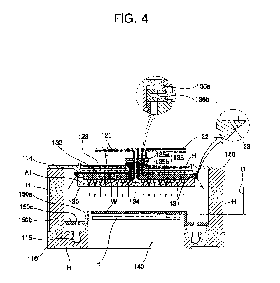
- the reactor 100 includes a reactor block 110 on which a wafer is placed, a shower head plate 120 coupled to the reactor block 110 using hinges 128 and 129, a diffusion plate 130 installed on the shower head plate 120 for spraying a reaction gas and/or inert gas, and a wafer block 140 installed within the reactor block 110, on which a wafer is seated.
- a first connection line 121 for transferring a supplied first reaction gas and/or inert gas, and a second connection line 122 for transferring a supplied second reaction gas and/or inert gas, are installed on the shower head plate 120.
- First and second connection pipes 111 and 112 are installed on the reactor block 110, and connected to first and second reaction gas supply lines 220 and 240, respectively, to be described later.
- the first and second connection pipes 111 and 112 are connected to the first and second connection lines 121 and 122 installed on the shower head plate 120 via a connecting portion 113 and an O-ring 113a so that they are sealed.
- At least two exhaust holes 117 and 118 for exhausting introduced inert gases and/or reaction gases are formed to be symmetrical to each other on the bottom of the reactor block 110.
- a main O-ring 114 is installed on the upper surface of the reactor block 110, so that the reactor block 110 and the shower head plate 120 are securely sealed when the shower head plate 120 is covered.
- the shower head plate 120 covers the reactor block 110, so that a predetermined pressure is constantly maintained within the reactor block 110. Also, the shower head plate 120 covers the reactor block 110 so that the diffusion plate 130 is placed within the reactor block 110.
- the diffusion plate 130 which sprays a gas during a thin film deposition process, has a plurality of spray holes 131, which are connected to the first connection line 121, and spray a first reaction gas and/or inert gas over the wafer block 140, and a plurality of nozzles 133, which are connected to a passage 132 leading to the second connection line 122 and face the inner sidewall of the reactor block 110 to spray a second reaction gas and/or inert gas onto the edges of the wafer block 140.
- a first mixing portion 134 for evenly mixing a first reaction gas and an inert gas and flowing the mixture to the spray hole 131 is formed at the center of the inside of the diffusion plate 130, as shown in FIGS. 4 and 5.
- the first reaction gas and the inert gas flowing via the connection line 121 are swirled and mixed, and then diffused and evenly sprayed onto the wafer via all of the spray holes 131.
- Spray holes 131 are not formed below the first mixing portion 134 in the diffusion plate 130.
- the entire area of the diffusion plate 130 having the spray holes 131 is larger than the area of a wafer w seated on the wafer block 140, so that a gas can be evenly spayed over the entire surface of the wafer.
- the nozzles 133 lead to the passages 132 radially formed from a second mixing portion 135, and are slanted toward the inner sidewall of the reactor block 110, as shown in FIG. 4.
- the second mixing portion 135 for evenly mixing a second reaction gas and an inert gas is formed between the second connection line 122 and the shower head plate 120, as shown in FIG. 4.
- the second mixing portion 135 has a structure in which a hole 135b is formed through a partition 135a.
- the wafer block 140 on which a wafer w is safely seated, has a heater H installed in the wafer block 140 to heat and maintain the wafer block 140 to a predetermined temperature during deposition.
- the interval (D) between the diffusion plate 130 and the wafer block 140 is in the range of 20mm to 50mm.
- FIG. 6 which is a graph showing the interval (D) and specific resistance during deposition of a thin film, it can be seen that the specific resistance is the lowest when the interval (D) between the diffusion plate 130 and the wafer block 140 is 30mm.
- specific resistance values were low at the intervals D within a range of about 20 to 50mm, and it can be concluded that the interval D is an important structural property in forming an excellent thin film.
- the interval within this range is compared to a conventional chemical vapor deposition (CVD) reactor in which the interval between a diffraction plate to which a reaction gas is sprayed and a wafer block on which a wafer is seated is about 50 to 100mm.
- CVD chemical vapor deposition
- the interval D is smaller than that in the prior art, a dense first reaction gas layer is formed on a wafer w by the pressure of a first reaction gas and/or inert gas sprayed from the spray holes 131.
- the first reaction gas layer reacts with a second reaction gas flowed in later, so that a thin film having a higher purity and an excellent electrical property can be formed.
- a pumping baffle 150 is installed around the wafer block 140.
- the pumping baffle 150 is made up of a sidewall 150a installed on the lateral side of the wafer block 140, and a bottom wall 150b through which symmetrical holes 150c are formed.
- a donut-shaped pumping pot 115 connected to an exhaust line is formed below the bottom wall 150b of the pumping baffle 150, that is, on the bottom of the reactor block 110.
- the sidewall 150a and the bottom wall 150b of the pumping baffle 150 provide a space in which a second reaction gas and/or inert gas sprayed toward the inner sidewall of the reactor block 110 can more evenly react to the first reaction gas layer formed on the wafer w seated on the wafer block 140.
- a process product generated during deposition of a thin film, and gases not used during deposition of a thin film are slipped through the hole 150c. These gases pass through the exhaust holes 117 and 118, and are exhausted via the pumping pot 115.
- the pressure within a reactor must be maintained to be 1 to 10 torr.
- a pressure measuring portion 160 must be installed within the reactor.
- the above-described thin film deposition reactor has heaters (H) formed inside and outside to heat the reactor when a thin film is deposited.
- H heaters
- the temperature of the inner surface of the reactor block 110 must be kept at about 120 to 200 °C, and the temperature of the diffusion plate 130 must be kept at about 150 to 260°C.
- the wafer block 140 must be kept at a temperature of about 425 to 650°C, and the pumping baffle 150 must be kept at a temperature of about 150 to 230°C.
- the temperature of a vat valve 101 between the reactor 100 and a transfer module 102 for supplying and transferring a wafer w must be maintained at about 140 to 170°C. Such a temperature setting can minimize formation of process byproducts.
- a coolant passage 123 for allowing a coolant, to flow is formed on the shower head plate 120.
- the temperature of the diffusion plate 130 can be lowered within a desired range by flowing a coolant such as oil, water or air through the coolant passage 123.
- the inside temperature of the reactor 100 is important.
- an excessive thin film or process byproduct is deposited on the surface of the diffusion plate 130.
- the temperature of the diffusion plate 130 is also an important variable, and this will now be described with reference to FIG. 7.
- FIG. 7 is a graph showing the relationship between the bottom temperature of the diffusion plate 130 and the speed of deposition of a TiN thin film, when a TiN film is deposited using a TiCl 4 gas and an NH 3 gas.
- T 2 is greater than T 1 .
- FIG. 7 is a graph showing the relationship between the bottom temperature of the diffusion plate 130 and the speed of deposition of a TiN thin film, when a TiN film is deposited using a TiCl 4 gas and an NH 3 gas.
- a thin film or process byproduct deposited on the bottom of a diffusion plate can be minimized by voluntarily increasing or decreasing the temperature of the diffusion plate 130.
- particles and undesired influences upon the process can be excluded, so finally a cleaning period can be increased, and a cleaning effect can be improved.
- the thin film deposition reactor having such a configuration is combined with a transfer module 102 for supplying and transferring a wafer w , having a vat valve 101 between them.
- the wafer w is transferred into the reactor 100 via a wafer transfer hole 116 using a robot arm (not shown) and seated on the wafer block 140, as shown in FIG. 8.
- the gas jungle includes a first reaction gas supply portion 210 for supplying a reaction gas to the reactor 100, and a second reaction gas supply portion 230 for supplying a second gas to the reaction gas 100.
- the first reaction gas supply portion 210 is connected to the reactor 100 via a first reaction gas supply line 220
- the second reaction gas supply portion 230 is connected to the reactor 100 via a second reaction gas supply line 240.
- a first inert gas supply line 260 through which an inert gas supplied from the inert gas supply source 250 is transferred is connected to the first reaction gas supply line 220
- a second inert gas supply line 270 through which an inert gas supplied from the inert gas supply source 250 is transferred is connected to the second reaction gas supply line 240.
- the first reaction gas supply portion 210 includes a bubbler 211 for gasifying a first reaction material, a first reaction gas mass flow controller (MFC) 212 for controlling the flow of a first reaction gas supplied from the bubbler 211, and first and second valves V1 and V2 installed on the line between the bubbler 211 and the first reaction gas MFC 212 for allowing or blocking the flow of a first reaction gas.
- a third valve V3 for allowing or blocking the flow of the first reaction gas controlled by the first reaction gas MFC 212 is installed on the first reaction gas supply line 220.
- the second reaction gas supply portion 230 includes a fourth valve V4 for allowing or blocking the flow of a second reaction gas, and a second reaction gas MFC 232 for controlling the flow of a second reaction gas passed through the fourth valve V4.
- a fifth valve V5 for allowing or blocking the flow of a second reaction gas controlled by the second reaction gas MFC 232 is installed on the second reaction gas supply line 240.
- a sixth valve V6 for allowing or blocking the flow of a supplied inert gas, a first inert gas MFC 262 for controlling the flow of an inert gas passed through the sixth valve V6, and a seventh valve V7 for allowing or blocking the flow of an inert gas controlled by the first inert gas MFC 262, are installed on the first inert gas supply line 260.
- An eighth valve V8 for allowing or blocking the flow of a supplied inert gas, a second inert gas MFC 272 for controlling the flow of an inert gas passed through the eighth valve V8, and a ninth valve V9 for allowing or blocking the flow of an inert gas controlled by the second inert gas MFC 272, are installed on the second inert gas supply line 270.
- the gas jungle includes a first bypass line 280 for allowing a first reaction gas and/or inert gas to flow directly to the exhaust line 400 without passing through the reactor 100, and a second bypass line 290 for allowing a second reaction gas and/or inert gas to flow directly to the exhaust line 400 without passing through the reactor 100.
- the first bypass line 280 has a tenth valve V10 connected to the line between the first reaction gas MFC 212 and the third valve V3 for allowing or blocking the flow of a first reaction gas to the exhaust line 400, and an eleventh valve V11 connected to the line between the first inert gas MFC 262 and the seventh valve V7 for allowing or blocking the flow of an inert gas to the exhaust line 400.
- the second bypass line 290 has a twelfth valve V12 connected to the line between the second reaction gas MFC 232 and the fifth valve V5 for allowing or blocking the flow of a second reaction gas to the exhaust line 400, and a thirteenth valve V13 connected to the line between the second inert gas MFC 272 and the ninth valve V9 for allowing or blocking the flow of an inert gas to the exhaust line 400.
- the first and second bypass lines 280 and 290 are adopted to purge the lines within the gas jungle, when a small amount of gas flowed in while a material of a first or second reaction gas or an inert gas is exchanged must flow directly to the exhaust line 400 without passing by the reactor 100, when a contaminating source is generated within the lines, or when a new gas jungle is replaced.
- first and second reaction gases, air or contaminating sources remaining within lines are purged directly to the exhaust line 400 via the first and second bypass lines 280 and 290 by an inert gas, so that the reactor 100 can be prevented from being contaminated.
- the first and second bypass lines 280 and 290 are not used in processes for depositing a thin film, but used only in specific cases.
- the gas jungle further includes a separate inert gas supply line 320 for supplying an inert gas from the inert gas supply source 310 in order to purge gases and/or contaminating sources remaining in the lines.
- the inert gas supply line 320 is organically connected to the first and second reaction gas supply portions 210 and 230, the first and second inert gas supply lines 260 and 270, the first and second bypass lines 280 and 290, and the exhaust line 400.
- the inert gas supply line 320 is connected to gas lines fundamentally required by a process, via a fourteenth valve V14 for allowing or blocking the flow of an inert gas to the first reaction gas supply portion 210, a fifteenth valve V15 for allowing or blocking the flow of an inert gas to the second reaction gas supply portion 230, a sixteenth valve V16 for allowing or blocking the flow of an inert gas to the first inert gas supply line 260, a seventeenth valve V17 for allowing or blocking the flow of an inert gas to the second inert gas supply line 270, an eighteenth valve V18 for allowing or blocking the flow of an inert gas to the first bypass line 280, and a nineteenth valve V19 for allowing or blocking the flow of an inert gas to the second bypass line 290.
- a fourteenth valve V14 for allowing or blocking the flow of an inert gas to the first reaction gas supply portion 210
- a fifteenth valve V15 for allowing or blocking the flow of an in
- the reactor 100, the first and second bypass lines 280 and 290 and a cleaning gas supply line 340 to be described later as a feature of the present invention are connected to the exhaust line 400.
- a throttle valve TV controlled by the internal pressure of the reactor 100 measured by the pressure measuring portion 160, for controlling the amount of an exhausted gas, is installed on the exhaust line 400.
- Twenty third, twenty fourth and twenty fifth valves V23, V24 and V25 for allowing or blocking the flow of an exhausted gas are also installed on the exhaust line 400.
- the first bypass line 280 is connected to the line between the twenty third and twenty fourth valves V23 and V24
- the second bypass line 290 is connected to the line between the twenty fifth valve V25 and the exhaust pump 410.
- a cold spot due to undesired condensation occurring when a reaction gas flows may be formed.
- heaters (not shown) for preventing generation of a cold spot are installed on the lines.
- the heaters are independently installed at as many areas as possible along lines, and a temperature gradient is formed along a line.
- the temperature gradient is established to be within a range of 40 to 200°C toward the reactor 100.
- the gas jungle further includes a cleaning gas supply line 340 for cleaning the reactor 100.
- the cleaning gas supply line 340 is connected to the first reaction gas supply line 220, and includes a cleaning gas supply portion 330 for supplying a cleaning gas, a twenty first valve V21 for allowing or blocking the flow of a supplied cleaning gas, a cleaning gas MFC 342 for controlling the flow of a cleaning gas which has passed through the twenty first valve V21, and a twenty second valve V22 for allowing or blocking the flow of a cleaning gas which has been controlled by the cleaning gas MFC 342.
- a filter 332 for filtering out foreign materials existing within a cleaning gas is installed on the line between the cleaning gas supply portion 330 and the twenty first valve V21.
- a CIF 3 gas can be used as a cleaning gas.
- the cleaning gas supply line 340 is connected to the twenty sixth valve V26 and the second bypass line 290 connected to the exhaust line 400, in order to allow a cleaning gas to flow directly to the exhaust line 400 without passing through the reactor 100.
- a cleaning gas introduced via the cleaning gas supply line 340 is exhausted to the outside via the second bypass line 290 and the exhaust line 400, when the twenty second valve V22 is closed and the twenty sixth valve V26 is opened.
- This embodiment refers to a structure for depositing a TiN thin film on a wafer.
- TiCl 4 is used as a first reaction gas
- NH 3 is used as a second reaction gas
- Ar is used as an inert gas.
- liquid TiCl 4 is contained in the bubbler 211.
- the wafer w is transferred into the reactor 100 via the wafer transfer hole 116 using the robot arm (not shown) of the transfer module 102, and seated on the wafer block 140.
- the temperature of the wafer block 140 increases within a range of 425 to 650°C, so that the temperature of the wafer w is increased to 400 to 600°C.
- the step of introducing a gas into the reactor 100 is performed.
- the gas introducing step starts by opening the first valve V1, the sixth valve V6, the eighth valve V8, and the fourth valve V4 for several seconds. Then, a bubbled TiCl 4 gas is filled up to the second valve V2, and Ar gas is filled up to the seventh and ninth valves V7 and V9 after its amount is appropriately controlled by the first and second inert gas MFCs 262 and 272. An NH 3 gas is filled up to the fifth valve V5 after its amount is appropriately controlled by the second reaction gas MFC 232.
- an Ar gas is flowed into the reactor 100 through the seventh and ninth valves V7 and V9.
- the internal pressure of the reactor 100 is kept at 10 - 4 ⁇ 5x10 -3 torr.
- the internal pressure of the reactor 100 is 1 to 10 torr. This pressure is obtained by the pressure measuring portion 160 installed in the reactor 100 appropriately opening the throttle valve TV of the exhaust line 400.
- the reason why the seventh and ninth valves V7 and V9 are opened after the sixth and eighth valves V6 and V8 are opened is that the gas within the reactor 100 may flow backward through the seventh and ninth valves V7 and V9 when they are suddenly opened.
- a TiN thin film is deposited on a wafer w by alternately introducing a TiCl 4 gas and an NH 3 gas into the reactor 100.
- a TiCl 4 gas is introduced first, a TiCl 4 gas and an Ar gas are first introduced into the reactor, in the first step. After a predetermined period of time, the TiCl 4 gas is excluded.
- a TiCl 4 layer is formed on the wafer w , and compressed by an Ar gas which is continuously introduced.
- an NH 3 gas and an Ar gas are introduced together.
- the supply of the NH 3 gas is blocked for a predetermined period of time.
- the NH 3 gas reacts to the TiCl 4 layer previously formed on the wafer w, thereby forming the TiN thin film on the wafer w. That is, a TiN + NH 3 layer is formed by the consecutive first and second steps.
- the first step is again performed to continuously grow a thin film on the TiN + NH 3 layer.
- the TiN + NH 3 layer is changed to a TiN+TiN+TiCl 4 layer.
- the second step is performed to form a TiN+TiN+TiN+NH 3 layer.
- a TiN thin film having a desired thickness can be obtained by repeating this process.
- This TiN thin film deposition process is performed by alternately opening and closing the third and fifth valves V3 and V5 in a state where the first and fourth valves V1 and V4 are always open, while an Ar gas is continuously introduced into the reactor 100 by opening the sixth, seventh, eighth and ninth valves V6, V7, V8 and V9.
- the second valve V2 is opened before the third valve V3, so that a TiCl 4 gas passes through the first reaction gas MFC 212 and is filled up to the third valve V3. Thereafter, when the third valve V3 is opened to send a first reaction gas to the reactor 100, the second valve V2 is closed. That is, the first reaction gas flows to the first reaction gas supply line 220 by sequentially passing through valves. A process byproduct gas generated during reaction is exhausted via the throttle valve TV of the exhaust line 400, and the twenty third, twenty fourth and twenty fifth valves V23, V24 and V25.
- a TiCl 4 gas flows to the first reaction gas supply line 220 via the third valve V3 after its flow is controlled by the first and second valves V1 and V2, and an Ar gas is controlled in its flow, passes through the seventh valve V7, is mixed with the TiCl 4 gas on the first reaction gas supply line 220, and flows to the reactor 100.
- a mixture of TiCl 4 and Ar pass through the first connection pipe 111 and the first connection line 121, is evenly mixed once more in the first mixing portion 134, and is evenly sprayed over the wafer w through the spray holes 131.
- An NH 3 reaction gas is controlled in its flow through the fourth valve V4, and then flows to the second reaction gas supply line 240 via the fifth valve V5.
- An Ar gas is controlled in its flow, passes through the ninth valve V9, is mixed with an NH 3 gas on the second reaction gas supply line 240, and then flows to the reactor 100.
- a mixture of NH 3 and Ar pass through the second connection pipe 112 and the second connection line 122, is evenly mixed once more in the second mixing portion 135, and is sprayed toward the inner sidewall of the reactor block 110 through the nozzles 133.
- the flow of a TiCl 4 gas is 1SCCM or more
- the flow of an Ar gas to be mixed with a TiCl 4 gas is 50SCCM or more
- the flow of NH 3 is 50SCCM or more
- the flow of an Ar gas to be mixed with an NH 3 gas is 60SCCM or more.
- This thin film deposition is achieved by consecutive gas spraying to the reactor 100, and the process pressure of the reactor is kept constant by an appropriate signal exchange and control between a pressure measuring portion and valves including a throttle valve. Therefore, the uniformity of a deposited thin film is improved.
- a TaN thin film can be deposited on a wafer by the method described above.
- an inert gas such as the Ar gas adequately dilutes the first and second reaction gases and smoothly sends the diluted gases to the reactor 100, so this acts as an important process variable. Also, the inert gas prevents a gas from flowing backward to a corresponding reaction gas supply line, since more than a predetermined amount of inert gas always flows to the first and second reaction gas supply lines 220 and 240 during, before and after a thin film is deposited on a wafer.
- the cleaning method includes a main cleaning process and a sub cleaning process for removing a thin film or process byproduct from the inner wall and components of the reactor 100 using a flowing cleaning gas and inert gas, and a pre-coating process for attaching particles remaining within the reactor 100 to the inner wall and components of the reactor.
- the main cleaning process which is performed in a state where no wafers w is received by the reactor 100, is performed in a predetermined cycle or when the number of particles produced by excessive deposition of a thin film or process byproduct (powder, a thin film containing impurities, etc.) on the inner wall of the reactor 100 or several components (for example, a wafer block, the sidewall 150a of a pumping baffle, etc.) exceeds a predetermined value.
- the cleaning cycle varies according to the type of a formed thin film. However, when a TiN, Ti or TiAlN thin film is deposited, the main cleaning process is performed after at least 500 wafers are deposited.
- a cleaning gas controlled in its flow by the cleaning gas MFC 342, and an inert gas controlled in its flow by the first inert gas MFC 262 are mixed in the first reaction gas supply lines 220, and sprayed onto the wafer block 140 through the spray holes 131 of the diffusion plate 130, and an inert gas controlled in its flow by the second inert gas MFC 272 is sprayed to the edges of the wafer block 140 through the second reaction gas supply line 240 and the nozzles 133 of the diffusion plate 130.
- a ClF 3 gas is used as a cleaning gas
- an Ar gas is used as an inert gas.
- a ClF 3 gas is nearly colorless transparent at room temperature, and has a boiling point of 11.75°C.
- the ClF 3 gas must not be liquefied until it is introduced into the reactor 100, and heaters must be installed along lines to apply an appropriate temperature to the gas.
- An Ar gas adequately dilutes a ClF 3 gas by allowing the ClF 3 gas to flow to the diffusion plate 130 via the first reaction gas supply line 220, and allows the ClF 3 gas to smoothly flow into the reactor 100.
- the inside of the reactor must be set to a temperature which prevents damage to the material of the reactor due to excessive etching.
- Most of the components of the reactor are stable to a ClF 3 gas when they have a surface temperature of 170°C or less, and it is proper that the temperature of an exhaust line is also 170°C or less. Accordingly, heaters are controlled so that the surface temperature of the components of the reactor 100 except for the wafer block 140 does not exceed 200°C, preferably, is at 170°C or less.
- the main cleaning process is performed when the thin film deposition process temperature (425 to 650°C) of the wafer block 140 is lowered to about 300°C.
- the flow of the ClF 3 gas is controlled to 50SCCM or greater
- the flow of an Ar gas, which is mixed with the ClF 3 gas, and flows to the spray holes 131 is controlled to 50SCCM or greater
- an Ar gas flowing to the nozzles 133 via the second reaction gas supply line 240 is controlled to 300SCCM or greater.
- the inside pressure of the reactor 100 is set to a range of 0.5 to 10 torr. This gas cleaning process requires about 50 to 90 minutes.
- the sub cleaning process which is performed in a state where the reactor 100 receives no wafers, is more simplified than the main cleaning process which is performed when the number of particles produced by local excessive deposition within the reactor 100 although a sufficient amount of process byproduct is not deposited within the reactor 100 exceeds a predetermined number.
- the sub cleaning process denotes pulse introduction in which a ClF 3 gas is introduced into the reactor 100 by periodically opening and closing the twenty second valve V22.
- a ClF 3 gas causes a pressure fluctuation within the reactor 100, and etches out a thin film or process byproducts excessively deposited on local areas within the reactor 100 while being instantaneously evenly diffused due to the pressure fluctuation when being introduced into the reactor.
- the flow rate of the ClF 3 gas is controlled to 50SCCM or higher
- the flow rate of an Ar gas, which is mixed with the ClF 3 gas and flows to the spray holes 131 is controlled to 50SCCM or higher
- the flow rate of an Ar gas, which is mixed with the ClF 3 gas in the second reaction gas supply line 240 and flows to the nozzles 133 is controlled to 300SCCM or higher.
- a ClF 3 gas is introduced into the reactor 100 by periodically opening/closing the twenty second valve V22.
- the opening/closing period of the twenty second valve V22 is set to be about 1 to 2 seconds, and the total pulse introducing time is set to be about 5 minutes or more.
- the inside pressure of the reactor 100 is set to be within a range of 0.5 to 10 torr.
- the temperature of the wafer block 140 is set to be about 400°C or less, and the temperatures of the components of the reactor 100 except for the wafer block 140 are set to be at most 200°C, preferably, at 170°C or less.
- the pre-coating process is performed in a state where the reactor 100 receives no wafers, and adheres fine particles, which remain within the reactor 100 after the main cleaning process using a ClF 3 gas, to the inside surface of the reactor 100. This process prevents particles from dropping over a wafer during depositing a thin film.
- the gases within the reactor 100 must be sufficiently exhausted before the pre-coating process is performed.
- pumping is performed as much as possible by 100% opening the throttle valve TV while introduction of all gases into the reactor 100 is stopped, thereby rapidly exhausting remaining ClF 3 gas and Ar gas within the reactor 100 and remaining process byproducts to the exhaust line 400.
- the temperature of the wafer block 140 which has dropped during the main cleaning process, starts being increased to the thin film deposition process temperature of about 425 to 650°C. While the temperature of the wafer block 140 is increased, flushing for introducing an Ar gas into the reactor 100 is performed at the same time. Flushing is performed by opening the sixth and seventh valves V6 and V7 to allow an Ar gas to flow into the reactor 100 via the first reaction gas supply line 220 and simultaneously opening the eighth and ninth valves V8 and V9 to allow an Ar gas to flow into the reactor 100 via the second reaction gas supply line 240.
- the temperature of the wafer block 140 increases up to the thin film deposition process temperature.
- the pre-coating process which is similar to the thin film deposition process, is performed.
- the pre-coating process is performed by mixing a flow-controlled TiCl 4 gas and an Ar gas and spraying onto the wafer block 140 through the spray holes 131, and mixing an NH 3 gas and a flow-controlled Ar gas and spraying toward the edges of the wafer block 140 through the nozzles 133.
- an NH 3 gas is introduced at least several seconds before a TiCl 4 gas is introduced into the reactor, since a TiCl 4 gas is strongly erosive. If a TiCl 4 gas is first introduced into the reactor 100, it instantaneously etches the internal components of the reactor to thus generate very tiny solid particles. Thus, an NH 3 gas is introduced at least several seconds before a TiCl 4 gas is introduced, in order to pre-exist an NH 3 gas layer on the inside surface of the reactor 100, so that a TiCl 4 gas introduced reacts to the NH 3 gas. Therefore, etching is minimized.
- the NH 3 gas is introduced at least several seconds before the first reaction gas is introduced into the reaction gas, in order to minimize generation of particles.
- the first step of mixing and introducing the TiCl 4 gas and an Ar gas into the reactor 100 and excluding the TiCl 4 gas for a predetermined period of time, and the second step of introducing an NH 3 gas and an Ar gas into the reactor 100 and excluding the NH 3 gas for a predetermined period of time, are alternately repeated.
- the first step of mixing and introducing a TiCl 4 gas and an Ar gas and excluding the TiCl 4 gas for a predetermined period of time, while the NH 3 gas and an inert gas are continuously introduced is repeated. In this way, the pre-coating process is achieved.
- the pre-coating process is very similar to a thin film deposition process, except that it is performed in a state where no wafers are mounted within the reactor 100. Also, the pre-coating process is very similar to a thin film deposition process in terms of deposition conditions. That is, as in a thin film deposition process, when a compound gas containing a transfer metal element such as Ti, Ta or W is used as a first reaction gas, and an NH 3 gas is used as a second reaction gas, the temperature of the wafer w during thin film deposition is maintained at 400 to 600°C, and the temperature of lines connected to the reactor 100 is maintained at 40 to 200°C.
- a compound gas containing a transfer metal element such as Ti, Ta or W
- an NH 3 gas is used as a second reaction gas
- FIG. 9 shows the number of particles detected within a reactor before and after a cleaning process.
- reference character A denotes the number of particles detected after thin films are deposited on 500 wafers
- reference character B denotes the number of particles detected after the main cleaning process
- reference character C denotes the number of particles detected after the pre-coating process.
- 28 particles were detected after thin films are continuously deposited on 500 wafers
- 275 particles were detected after a 60-minute cleaning process
- 15 particles were detected after a 10-minute pre-coating process.
- the detection of 275 particles after the cleaning process shows not that the inside of the reactor 100 is contaminated, but that cleaning process byproducts existing within a diffusion plate during cleaning remain by failing to slipping to an exhaust line and drop over the wafer w . Thereafter, if the pre-coating process is performed, the number of particles detected can be significantly reduced.
- the above-described cleaning process is different from a conventional wet cleaning process, which is performed in a state where a reactor is opened, and can minimize a time loss caused during the wet cleaning process.
- the cleaning process can be performed at least five to ten times in a cycle of about 500 wafers or more.
- a second embodiment of ALD thin film deposition equipment having a cleaning apparatus according to the present invention will now be described with reference to FIG. 10.
- the same reference numerals as those in FIG. 1 denote the same elements.
- a thin film such as a WN thin film can be formed in the second embodiment.
- the first reaction gas supply portion 210 in the first embodiment is replaced with a first reaction gas supply portion 510.
- the first reaction gas supply portion 510 includes a thirty first valve V31 of allowing or blocking the flow of a first reaction gas, and a first reaction gas MFC 512 for controlling the flow of a first reaction gas which has passed through the thirty first valve V31.
- the first reaction gas supply portion 510 is connected to the third valve V3.
- a third embodiment of ALD thin film deposition equipment having a cleaning apparatus according to the present invention will now be described with reference to FIG. 11.
- the same reference numerals as those in FIG. 1 denote the same elements.
- the third embodiment further includes a third reaction gas transfer line for transferring a third reaction gas TriMethylAluminum (TMA) and a fourth reaction gas transfer line for transferring a fourth reaction gas H 2 .
- TMA TriMethylAluminum
- a fourth reaction gas supply portion 610 includes a thirty second valve V32 for allowing or blocking the flow of supplied H2, a fourth reaction gas MFC 612 for controlling the flow of H2 which has passed through the thirty second valve V32, and a thirty third valve V33 for allowing or blocking the flow of H2 controlled by the fourth reaction gas MFC 612.
- a third reaction gas supply portion 620 includes a bubbler 621 for gasifying a third reaction material, a third reaction gas MFC 622 for controlling the flow of a third reaction gas, a thirty fourth valve V34 installed on the line between the bubbler 621 and the third reaction gas MFC 622 for allowing or blocking the flow of the third reaction gas, and a thirty fifth valve V35 for allowing or blocking the flow of the third reaction gas, which has been controlled by the third reaction gas MFC 622, to the second reaction gas supply line 240.
- a compound gas containing a transfer metal element Ti or Ta is used as a first reaction gas
- an Ar gas is used as an inert gas
- a compound gas containing N is used as a second gas
- a TMA gas is used as a third reaction gas
- an H 2 gas is used as a fourth reaction gas.
- the third embodiment of the thin film deposition apparatus having such a configuration is almost the same as the first embodiment, so it will not be described in detail.
- Ti, TiN, TiAlN, WN and TaN thin films are mentioned as an ALD thin film. These embodiments are representative of the present invention. Thus, the present invention can also be applied when an ALD thin film containing a transfer metal element such as WSIN, TiSiN or TaSiN is deposited using changed reaction gases.
- a transfer metal element such as WSIN, TiSiN or TaSiN
- a thin film or process byproducts deposited within a reactor or on the surfaces of components of the reactor are effectively dry-cleaned without opening the reactor.
- a thin film deposition process can be easily performed after cleaning.
- a thin film such as Ti, TiAlN, TiN, TaN, WN, WSIN, TiSiN or TaSiN thin film is formed, a thin film and process byproducts can be effectively removed from the inner wall or components of a reactor during a cleaning process, after a thin film deposition process.
Abstract
An ALD thin film deposition equipment
and cleaning method wherein the reactor comprises:
Description
- The present invention relates to atomic layer deposition (ALD) thin film deposition equipment, and more particularly, to ALD thin film deposition equipment employing a cleaning apparatus and a cleaning method.
- Thin film deposition equipment forms a predetermined thin film on a wafer by supplying reaction gases to the wafer received within a reactor. This thin film deposition equipment includes chemical vapor deposition (CVD) thin film deposition equipment, atomic layer epitaxy (ALE) thin film deposition equipment, and others, and has been applied to various fields for manufacturing semiconductor devices.
- In thin film deposition equipment, a thin film is deposited not only on a wafer by an introduced reaction gas, but a thin film or process byproduct can also be deposited on the inner wall or component of a reactor, or on holes through which reaction gases are sprayed. When particles separated from the thin film or process byproduct drop on a wafer, the characteristics of a thin film deposited on the wafer are deteriorated. This requires a cleaning apparatus and method of effectively removing a thin film or a process byproduct deposited on the inner wall, components or holes of a reactor.
- An objective of the present invention is to provide an atomic layer deposition (ALD) thin film deposition equipment having a cleaning apparatus, and a cleaning method thereof, by which a thin film or process byproduct deposited within a reactor or on the surface of its component is effectively dry cleaned without opening the reactor, and then a thin film deposition process can be easily performed.
- To achieve the above objective, the present invention provides an atomic layer deposition (ALD) thin film deposition equipment having a cleaning apparatus, this equipment including: a
reactor 100 in which a wafer is mounted and a thin film is deposited on the wafer; a first reactiongas supply portion 210 for supplying a first reaction gas to thereactor 100; a second reactiongas supply portion 230 for supplying a second reaction gas to thereactor 100; a first reactiongas supply line 220 for connecting the first reactiongas supply portion 210 to thereactor 100; a second reactiongas supply line 240 for connecting the second reactiongas supply portion 230 to thereactor 100; a first inertgas supply line 260 for supplying an inert gas from an inertgas supply source 250 to the first reactiongas supply line 220; a second inertgas supply line 270 for supplying an inert gas from the inertgas supply source 250 to the second reactiongas supply line 240; anexhaust line 400 for exhausting the gas within therector 100 to the outside; and a cleaninggas supply line 340 connected to the first reactiongas supply line 220 for supplying a cleaning gas for cleaning thereactor 100. Here, the cleaning gas is ClF3. - Preferably, the cleaning
gas supply line 340 includes: a cleaning gas mass flow controller (MFC) for controlling the flow of a supplied cleaning gas; and at least one valve for allowing or blocking the flow of the cleaning gas. Also, preferably, the cleaninggas supply line 340 further includes a filter for filtering out foreign materials existing within the cleaning gas. - To achieve the above objective, the present invention provides a cleaning method for ALD thin film deposition equipment having a
reactor 100 including areactor block 110 on which a wafer is mounted, awafer block 140 installed within thereactor block 110, on which the wafer w is seated, and a diffusion plate having a plurality ofspray holes 131 formed over thewafer block 140 and a plurality ofnozzles 133 slanted toward the inner sidewall of thereactor block 110 to spray a gas toward the edges of thewafer block 140. This cleaning method includes a main cleaning process performed in a state where no wafers are received within thereactor 100, for spraying a mixture of a cleaning gas and an inert gas onto the wafer w through thespray holes 131 and spraying an inert gas toward the edges of thewafer block 140 through thenozzles 133. - Preferably, this cleaning method further includes a sub cleaning process performed in a state where no wafers are received within the reactor, for pulse-introducing the cleaning gas into the
reactor 100 to induce instantaneous diffusion due to a pressure fluctuation. Also, preferably, this cleaning method further includes a pre-coating process performed in a state where no wafers are received within the reactor, for adhering fine particles remaining within the reactor to the inside surface of the reactor. - The above objectives and advantages of the present invention will become more apparent by describing in detail preferred embodiments thereof with reference to the attached drawings in which:
- FIG. 1 is a schematic diagram of atomic layer deposition (ALD) thin film deposition equipment having a cleaning apparatus, according to a first embodiment of the present invention;
- FIG. 2 is an exploded perspective view of a reactor in the ALD thin film deposition equipment of FIG. 1;
- FIG. 3 is an exploded perspective view of a shower head and a diffusion plate in the reactor of FIG. 2;
- FIG. 4 is a cross-sectional view of the reactor of FIG. 2;
- FIG. 5 is a magnified cross-sectional view of the first mixing unit of the reactor of FIG. 4;
- FIG. 6 is a graph showing the relationship between an interval (D) and a specific resistance while a thin film is formed;
- FIG. 7 is a graph showing the relationship between the bottom temperature of a diffusion plate and the speed of deposition of a TiN thin film when a TiN film is deposited using a TiCl4 gas and an NH3 gas;
- FIG. 8 shows a reactor combined with a transfer module through a vat valve;
- FIG. 9 is a data showing the number of particles detected within a reactor after a cleaning process;
- FIG. 10 is a cross-sectional view of ALD thin film deposition equipment having a cleaning apparatus, according to a second embodiment of the present invention; and
- FIG. 11 is a cross-sectional view of ALD thin film deposition equipment having a cleaning apparatus, according to a third embodiment of the present invention.
-
- FIG. 1 shows atomic layer deposition (ALD) thin film deposition equipment having a cleaning apparatus, according to a first embodiment of the present invention. This ALD thin film deposition equipment can deposit a thin film, such as a TiN film or a TaN film, on a wafer. Deposition of a TiN thin film will now be described as an example. In order to form a TiN thin film, TiCl4 is used as a first reaction gas, NH3 is used as a second reaction gas, and Ar is used as an inert gas.
- Referring to FIG. 1, ALD thin film deposition equipment includes a
reactor 100 for receiving a wafer and depositing a thin film on the wafer, a gas jungle (this term was made by the present inventor to describe complicatedly-connected lines) for supplying a reaction gas to thereactor 100, and anexhaust line 400 for exhausting the gas within thereactor 100 to the outside. - FIG. 2 is an exploded perspective view of a reactor in the ALD thin film deposition equipment of FIG. 1. FIG. 3 is an exploded perspective view of the reactor of FIG. 2, in which a shower head plate is separated from a diffusion plate. FIG. 4 is a cross-sectional view of the reactor of FIG. 2, and FIG. 5 is a magnified cross-sectional view of the first mixing unit of the reactor of FIG. 4.
- Referring to FIGS. 2, 3, 4 and 5, the
reactor 100 includes areactor block 110 on which a wafer is placed, ashower head plate 120 coupled to thereactor block 110 usinghinges diffusion plate 130 installed on theshower head plate 120 for spraying a reaction gas and/or inert gas, and awafer block 140 installed within thereactor block 110, on which a wafer is seated. Afirst connection line 121 for transferring a supplied first reaction gas and/or inert gas, and asecond connection line 122 for transferring a supplied second reaction gas and/or inert gas, are installed on theshower head plate 120. - First and
second connection pipes reactor block 110, and connected to first and second reactiongas supply lines second connection pipes second connection lines shower head plate 120 via a connectingportion 113 and an O-ring 113a so that they are sealed. - At least two
exhaust holes reactor block 110. A main O-ring 114 is installed on the upper surface of thereactor block 110, so that thereactor block 110 and theshower head plate 120 are securely sealed when theshower head plate 120 is covered. - The
shower head plate 120 covers thereactor block 110, so that a predetermined pressure is constantly maintained within thereactor block 110. Also, theshower head plate 120 covers thereactor block 110 so that thediffusion plate 130 is placed within thereactor block 110. - The
diffusion plate 130, which sprays a gas during a thin film deposition process, has a plurality ofspray holes 131, which are connected to thefirst connection line 121, and spray a first reaction gas and/or inert gas over thewafer block 140, and a plurality ofnozzles 133, which are connected to apassage 132 leading to thesecond connection line 122 and face the inner sidewall of thereactor block 110 to spray a second reaction gas and/or inert gas onto the edges of thewafer block 140. - A
first mixing portion 134 for evenly mixing a first reaction gas and an inert gas and flowing the mixture to thespray hole 131 is formed at the center of the inside of thediffusion plate 130, as shown in FIGS. 4 and 5. The first reaction gas and the inert gas flowing via theconnection line 121 are swirled and mixed, and then diffused and evenly sprayed onto the wafer via all of thespray holes 131. -
Spray holes 131 are not formed below thefirst mixing portion 134 in thediffusion plate 130. Preferably, the entire area of thediffusion plate 130 having thespray holes 131 is larger than the area of a wafer w seated on thewafer block 140, so that a gas can be evenly spayed over the entire surface of the wafer. - The
nozzles 133 lead to thepassages 132 radially formed from a second mixing portion 135, and are slanted toward the inner sidewall of thereactor block 110, as shown in FIG. 4. - The second mixing portion 135 for evenly mixing a second reaction gas and an inert gas is formed between the
second connection line 122 and theshower head plate 120, as shown in FIG. 4. The second mixing portion 135 has a structure in which ahole 135b is formed through apartition 135a. - The
wafer block 140, on which a wafer w is safely seated, has a heater H installed in thewafer block 140 to heat and maintain thewafer block 140 to a predetermined temperature during deposition. - The interval (D) between the
diffusion plate 130 and thewafer block 140 is in the range of 20mm to 50mm. Referring to FIG. 6, which is a graph showing the interval (D) and specific resistance during deposition of a thin film, it can be seen that the specific resistance is the lowest when the interval (D) between thediffusion plate 130 and thewafer block 140 is 30mm. However, when other conditions, for example, the types and amounts of first and second reaction gases, the temperature of a wafer block, or the like, were changed, specific resistance values were low at the intervals D within a range of about 20 to 50mm, and it can be concluded that the interval D is an important structural property in forming an excellent thin film. - The interval within this range is compared to a conventional chemical vapor deposition (CVD) reactor in which the interval between a diffraction plate to which a reaction gas is sprayed and a wafer block on which a wafer is seated is about 50 to 100mm. In the present invention, since the interval D is smaller than that in the prior art, a dense first reaction gas layer is formed on a wafer w by the pressure of a first reaction gas and/or inert gas sprayed from the
spray holes 131. The first reaction gas layer reacts with a second reaction gas flowed in later, so that a thin film having a higher purity and an excellent electrical property can be formed. - A pumping
baffle 150 is installed around thewafer block 140. The pumpingbaffle 150 is made up of asidewall 150a installed on the lateral side of thewafer block 140, and abottom wall 150b through whichsymmetrical holes 150c are formed. A donut-shapedpumping pot 115 connected to an exhaust line is formed below thebottom wall 150b of the pumpingbaffle 150, that is, on the bottom of thereactor block 110. - The
sidewall 150a and thebottom wall 150b of the pumpingbaffle 150 provide a space in which a second reaction gas and/or inert gas sprayed toward the inner sidewall of thereactor block 110 can more evenly react to the first reaction gas layer formed on the wafer w seated on thewafer block 140. A process product generated during deposition of a thin film, and gases not used during deposition of a thin film are slipped through thehole 150c. These gases pass through the exhaust holes 117 and 118, and are exhausted via the pumpingpot 115. - When a thin film is deposited, the pressure within a reactor must be maintained to be 1 to 10 torr. In order to observe and control this pressure, a
pressure measuring portion 160 must be installed within the reactor. - The above-described thin film deposition reactor has heaters (H) formed inside and outside to heat the reactor when a thin film is deposited. For example, in a TiN thin film deposition process, when a TiN thin film is deposited, the temperature of the inner surface of the
reactor block 110 must be kept at about 120 to 200 °C, and the temperature of thediffusion plate 130 must be kept at about 150 to 260°C. Also, thewafer block 140 must be kept at a temperature of about 425 to 650°C, and thepumping baffle 150 must be kept at a temperature of about 150 to 230°C. The temperature of avat valve 101 between thereactor 100 and atransfer module 102 for supplying and transferring a wafer w must be maintained at about 140 to 170°C. Such a temperature setting can minimize formation of process byproducts. - A
coolant passage 123 for allowing a coolant, to flow is formed on theshower head plate 120. The temperature of thediffusion plate 130 can be lowered within a desired range by flowing a coolant such as oil, water or air through thecoolant passage 123. - During a thin film deposition process, the inside temperature of the
reactor 100 is important. When the inside temperature of thereactor 100 departs an optimum temperature range, an excessive thin film or process byproduct is deposited on the surface of thediffusion plate 130. Thus, many particles drop on the wafer, and thediffusion plate 130 is eroded. Accordingly, the temperature of thediffusion plate 130 is also an important variable, and this will now be described with reference to FIG. 7. - FIG. 7 is a graph showing the relationship between the bottom temperature of the
diffusion plate 130 and the speed of deposition of a TiN thin film, when a TiN film is deposited using a TiCl4 gas and an NH3 gas. A graph when the bottom temperature of thediffusion plate 130 is T1, and a graph when the bottom temperature of thediffusion plate 130 is T2, are shown in FIG. 7. Here, T2 is greater than T1. As shown in the graph of FIG. 7, when the temperature of thediffusion plate 130 exceeds the optimum temperature range, that is, when T1 < T2, a greater amount of TiCl4 gas must be introduced into thereactor 100 to obtain the same deposition speed of a TiN thin film, since a relatively greater amount of TiCl4 gas are used to produce particles by reacting to the bottom of thediffusion plate 130 or to deposit a thin film on thediffusion plate 130, instead of being used to deposit a thin film on a wafer w. Accordingly, the increased temperature of thediffusion plate 130 needs to be easily lowered as necessary. In this case, the temperature of thediffusion plate 130 can be reduced by allowing a coolant to flow to thecoolant passage 123 formed on theshower head plate 120. Consequently, during depositing a thin film, a thin film or process byproduct deposited on the bottom of a diffusion plate can be minimized by voluntarily increasing or decreasing the temperature of thediffusion plate 130. Thus, particles and undesired influences upon the process can be excluded, so finally a cleaning period can be increased, and a cleaning effect can be improved. - The thin film deposition reactor having such a configuration is combined with a
transfer module 102 for supplying and transferring a wafer w, having avat valve 101 between them. The wafer w is transferred into thereactor 100 via awafer transfer hole 116 using a robot arm (not shown) and seated on thewafer block 140, as shown in FIG. 8. - As shown in FIG. 1, the gas jungle includes a first reaction
gas supply portion 210 for supplying a reaction gas to thereactor 100, and a second reactiongas supply portion 230 for supplying a second gas to thereaction gas 100. The first reactiongas supply portion 210 is connected to thereactor 100 via a first reactiongas supply line 220, and the second reactiongas supply portion 230 is connected to thereactor 100 via a second reactiongas supply line 240. A first inertgas supply line 260 through which an inert gas supplied from the inertgas supply source 250 is transferred is connected to the first reactiongas supply line 220, and a second inertgas supply line 270 through which an inert gas supplied from the inertgas supply source 250 is transferred is connected to the second reactiongas supply line 240. - The first reaction
gas supply portion 210 includes abubbler 211 for gasifying a first reaction material, a first reaction gas mass flow controller (MFC) 212 for controlling the flow of a first reaction gas supplied from thebubbler 211, and first and second valves V1 and V2 installed on the line between thebubbler 211 and the firstreaction gas MFC 212 for allowing or blocking the flow of a first reaction gas. A third valve V3 for allowing or blocking the flow of the first reaction gas controlled by the firstreaction gas MFC 212 is installed on the first reactiongas supply line 220. - The second reaction
gas supply portion 230 includes a fourth valve V4 for allowing or blocking the flow of a second reaction gas, and a secondreaction gas MFC 232 for controlling the flow of a second reaction gas passed through the fourth valve V4. A fifth valve V5 for allowing or blocking the flow of a second reaction gas controlled by the secondreaction gas MFC 232 is installed on the second reactiongas supply line 240. - A sixth valve V6 for allowing or blocking the flow of a supplied inert gas, a first
inert gas MFC 262 for controlling the flow of an inert gas passed through the sixth valve V6, and a seventh valve V7 for allowing or blocking the flow of an inert gas controlled by the firstinert gas MFC 262, are installed on the first inertgas supply line 260. - An eighth valve V8 for allowing or blocking the flow of a supplied inert gas, a second
inert gas MFC 272 for controlling the flow of an inert gas passed through the eighth valve V8, and a ninth valve V9 for allowing or blocking the flow of an inert gas controlled by the secondinert gas MFC 272, are installed on the second inertgas supply line 270. - Here, the gas jungle includes a
first bypass line 280 for allowing a first reaction gas and/or inert gas to flow directly to theexhaust line 400 without passing through thereactor 100, and asecond bypass line 290 for allowing a second reaction gas and/or inert gas to flow directly to theexhaust line 400 without passing through thereactor 100. - The
first bypass line 280 has a tenth valve V10 connected to the line between the firstreaction gas MFC 212 and the third valve V3 for allowing or blocking the flow of a first reaction gas to theexhaust line 400, and an eleventh valve V11 connected to the line between the firstinert gas MFC 262 and the seventh valve V7 for allowing or blocking the flow of an inert gas to theexhaust line 400. - The
second bypass line 290 has a twelfth valve V12 connected to the line between the secondreaction gas MFC 232 and the fifth valve V5 for allowing or blocking the flow of a second reaction gas to theexhaust line 400, and a thirteenth valve V13 connected to the line between the secondinert gas MFC 272 and the ninth valve V9 for allowing or blocking the flow of an inert gas to theexhaust line 400. - The first and
second bypass lines exhaust line 400 without passing by thereactor 100, when a contaminating source is generated within the lines, or when a new gas jungle is replaced. As described above, first and second reaction gases, air or contaminating sources remaining within lines are purged directly to theexhaust line 400 via the first andsecond bypass lines reactor 100 can be prevented from being contaminated. Thus, the first andsecond bypass lines - The gas jungle further includes a separate inert
gas supply line 320 for supplying an inert gas from the inertgas supply source 310 in order to purge gases and/or contaminating sources remaining in the lines. The inertgas supply line 320 is organically connected to the first and second reactiongas supply portions gas supply lines second bypass lines exhaust line 400. The inertgas supply line 320 is connected to gas lines fundamentally required by a process, via a fourteenth valve V14 for allowing or blocking the flow of an inert gas to the first reactiongas supply portion 210, a fifteenth valve V15 for allowing or blocking the flow of an inert gas to the second reactiongas supply portion 230, a sixteenth valve V16 for allowing or blocking the flow of an inert gas to the first inertgas supply line 260, a seventeenth valve V17 for allowing or blocking the flow of an inert gas to the second inertgas supply line 270, an eighteenth valve V18 for allowing or blocking the flow of an inert gas to thefirst bypass line 280, and a nineteenth valve V19 for allowing or blocking the flow of an inert gas to thesecond bypass line 290. - The
reactor 100, the first andsecond bypass lines gas supply line 340 to be described later as a feature of the present invention are connected to theexhaust line 400. A throttle valve TV controlled by the internal pressure of thereactor 100 measured by thepressure measuring portion 160, for controlling the amount of an exhausted gas, is installed on theexhaust line 400. Twenty third, twenty fourth and twenty fifth valves V23, V24 and V25 for allowing or blocking the flow of an exhausted gas are also installed on theexhaust line 400. Her, thefirst bypass line 280 is connected to the line between the twenty third and twenty fourth valves V23 and V24, and thesecond bypass line 290 is connected to the line between the twenty fifth valve V25 and theexhaust pump 410. - In this gas jungle, a cold spot due to undesired condensation occurring when a reaction gas flows may be formed. Since a cold spot badly affects the process for depositing a thin film, heaters (not shown) for preventing generation of a cold spot are installed on the lines. Preferably, the heaters are independently installed at as many areas as possible along lines, and a temperature gradient is formed along a line. In this embodiment, the temperature gradient is established to be within a range of 40 to 200°C toward the
reactor 100. - The gas jungle further includes a cleaning
gas supply line 340 for cleaning thereactor 100. The cleaninggas supply line 340 is connected to the first reactiongas supply line 220, and includes a cleaninggas supply portion 330 for supplying a cleaning gas, a twenty first valve V21 for allowing or blocking the flow of a supplied cleaning gas, a cleaninggas MFC 342 for controlling the flow of a cleaning gas which has passed through the twenty first valve V21, and a twenty second valve V22 for allowing or blocking the flow of a cleaning gas which has been controlled by the cleaninggas MFC 342. Here, afilter 332 for filtering out foreign materials existing within a cleaning gas is installed on the line between the cleaninggas supply portion 330 and the twenty first valve V21. In the above-described structure, a CIF3 gas can be used as a cleaning gas. - Here, the cleaning
gas supply line 340 is connected to the twenty sixth valve V26 and thesecond bypass line 290 connected to theexhaust line 400, in order to allow a cleaning gas to flow directly to theexhaust line 400 without passing through thereactor 100. A cleaning gas introduced via the cleaninggas supply line 340 is exhausted to the outside via thesecond bypass line 290 and theexhaust line 400, when the twenty second valve V22 is closed and the twenty sixth valve V26 is opened. - The operation of the first embodiment of ALD thin film deposition equipment having a cleaning apparatus with such a structure will now be described. This embodiment refers to a structure for depositing a TiN thin film on a wafer. To achieve this embodiment, TiCl4 is used as a first reaction gas, NH3 is used as a second reaction gas, and Ar is used as an inert gas. Thus, liquid TiCl4 is contained in the
bubbler 211. - The wafer w is transferred into the
reactor 100 via thewafer transfer hole 116 using the robot arm (not shown) of thetransfer module 102, and seated on thewafer block 140. - When the wafer w is seated on the
wafer block 140, the temperature of thewafer block 140 increases within a range of 425 to 650°C, so that the temperature of the wafer w is increased to 400 to 600°C. After the wafer temperature is stabilized, the step of introducing a gas into thereactor 100 is performed. - The gas introducing step starts by opening the first valve V1, the sixth valve V6, the eighth valve V8, and the fourth valve V4 for several seconds. Then, a bubbled TiCl4 gas is filled up to the second valve V2, and Ar gas is filled up to the seventh and ninth valves V7 and V9 after its amount is appropriately controlled by the first and second
inert gas MFCs reaction gas MFC 232. - Next, an Ar gas is flowed into the
reactor 100 through the seventh and ninth valves V7 and V9. Before the Ar gas is introduced, the internal pressure of thereactor 100 is kept at 10- 4∼5x10⁻³ torr. However, as the Ar gas is introduced, the internal pressure of thereactor 100 is 1 to 10 torr. This pressure is obtained by thepressure measuring portion 160 installed in thereactor 100 appropriately opening the throttle valve TV of theexhaust line 400. Here, the reason why the seventh and ninth valves V7 and V9 are opened after the sixth and eighth valves V6 and V8 are opened is that the gas within thereactor 100 may flow backward through the seventh and ninth valves V7 and V9 when they are suddenly opened. - Thereafter, a TiN thin film is deposited on a wafer w by alternately introducing a TiCl4 gas and an NH3 gas into the
reactor 100. For example, when a TiCl4 gas is introduced first, a TiCl4 gas and an Ar gas are first introduced into the reactor, in the first step. After a predetermined period of time, the TiCl4 gas is excluded. Thus, a TiCl4 layer is formed on the wafer w, and compressed by an Ar gas which is continuously introduced. - In the second step, an NH3 gas and an Ar gas are introduced together. The supply of the NH3 gas is blocked for a predetermined period of time. The NH3 gas reacts to the TiCl4 layer previously formed on the wafer w, thereby forming the TiN thin film on the wafer w. That is, a TiN + NH3 layer is formed by the consecutive first and second steps.
- Next, the first step is again performed to continuously grow a thin film on the TiN + NH3 layer. Then, the TiN + NH3 layer is changed to a TiN+TiN+TiCl4 layer. Thereafter, the second step is performed to form a TiN+TiN+TiN+NH3 layer. A TiN thin film having a desired thickness can be obtained by repeating this process.
- This TiN thin film deposition process is performed by alternately opening and closing the third and fifth valves V3 and V5 in a state where the first and fourth valves V1 and V4 are always open, while an Ar gas is continuously introduced into the
reactor 100 by opening the sixth, seventh, eighth and ninth valves V6, V7, V8 and V9. - Here, the second valve V2 is opened before the third valve V3, so that a TiCl4 gas passes through the first
reaction gas MFC 212 and is filled up to the third valve V3. Thereafter, when the third valve V3 is opened to send a first reaction gas to thereactor 100, the second valve V2 is closed. That is, the first reaction gas flows to the first reactiongas supply line 220 by sequentially passing through valves. A process byproduct gas generated during reaction is exhausted via the throttle valve TV of theexhaust line 400, and the twenty third, twenty fourth and twenty fifth valves V23, V24 and V25. - To sum up the above-described reaction, a TiCl4 gas flows to the first reaction
gas supply line 220 via the third valve V3 after its flow is controlled by the first and second valves V1 and V2, and an Ar gas is controlled in its flow, passes through the seventh valve V7, is mixed with the TiCl4 gas on the first reactiongas supply line 220, and flows to thereactor 100. - Thereafter, a mixture of TiCl4 and Ar pass through the
first connection pipe 111 and thefirst connection line 121, is evenly mixed once more in thefirst mixing portion 134, and is evenly sprayed over the wafer w through the spray holes 131. An NH3 reaction gas is controlled in its flow through the fourth valve V4, and then flows to the second reactiongas supply line 240 via the fifth valve V5. An Ar gas is controlled in its flow, passes through the ninth valve V9, is mixed with an NH3 gas on the second reactiongas supply line 240, and then flows to thereactor 100. Next, a mixture of NH3 and Ar pass through thesecond connection pipe 112 and thesecond connection line 122, is evenly mixed once more in the second mixing portion 135, and is sprayed toward the inner sidewall of thereactor block 110 through thenozzles 133. - Here, it is preferable that the flow of a TiCl4 gas is 1SCCM or more, the flow of an Ar gas to be mixed with a TiCl4 gas is 50SCCM or more, the flow of NH3 is 50SCCM or more, and the flow of an Ar gas to be mixed with an NH3 gas is 60SCCM or more. These values are obtained by several experiments. When the flow rates are at least as described above, a thin film having a high purity, an excellent electrical property, and a good step coverage can be obtained.
- This thin film deposition is achieved by consecutive gas spraying to the
reactor 100, and the process pressure of the reactor is kept constant by an appropriate signal exchange and control between a pressure measuring portion and valves including a throttle valve. Therefore, the uniformity of a deposited thin film is improved. - Also, when a compound gas containing Ta is used as a first reaction gas, and a compound gas containing N, for example, an NH3 gas, is used as a second reaction gas, a TaN thin film can be deposited on a wafer by the method described above.
- Here, an inert gas such as the Ar gas adequately dilutes the first and second reaction gases and smoothly sends the diluted gases to the
reactor 100, so this acts as an important process variable. Also, the inert gas prevents a gas from flowing backward to a corresponding reaction gas supply line, since more than a predetermined amount of inert gas always flows to the first and second reactiongas supply lines - Hereinafter, a cleaning method according to the present invention will be described. The cleaning method includes a main cleaning process and a sub cleaning process for removing a thin film or process byproduct from the inner wall and components of the
reactor 100 using a flowing cleaning gas and inert gas, and a pre-coating process for attaching particles remaining within thereactor 100 to the inner wall and components of the reactor. - The main cleaning process, which is performed in a state where no wafers w is received by the
reactor 100, is performed in a predetermined cycle or when the number of particles produced by excessive deposition of a thin film or process byproduct (powder, a thin film containing impurities, etc.) on the inner wall of thereactor 100 or several components (for example, a wafer block, thesidewall 150a of a pumping baffle, etc.) exceeds a predetermined value. The cleaning cycle varies according to the type of a formed thin film. However, when a TiN, Ti or TiAlN thin film is deposited, the main cleaning process is performed after at least 500 wafers are deposited. - In the main cleaning process, a cleaning gas controlled in its flow by the cleaning
gas MFC 342, and an inert gas controlled in its flow by the firstinert gas MFC 262 are mixed in the first reactiongas supply lines 220, and sprayed onto thewafer block 140 through the spray holes 131 of thediffusion plate 130, and an inert gas controlled in its flow by the secondinert gas MFC 272 is sprayed to the edges of thewafer block 140 through the second reactiongas supply line 240 and thenozzles 133 of thediffusion plate 130. In this embodiment, a ClF3 gas is used as a cleaning gas, and an Ar gas is used as an inert gas. - A ClF3 gas is nearly colorless transparent at room temperature, and has a boiling point of 11.75°C. The ClF3 gas must not be liquefied until it is introduced into the
reactor 100, and heaters must be installed along lines to apply an appropriate temperature to the gas. - An Ar gas adequately dilutes a ClF3 gas by allowing the ClF3 gas to flow to the
diffusion plate 130 via the first reactiongas supply line 220, and allows the ClF3 gas to smoothly flow into thereactor 100. - Upon the main cleaning process, the inside of the reactor must be set to a temperature which prevents damage to the material of the reactor due to excessive etching. Most of the components of the reactor are stable to a ClF3 gas when they have a surface temperature of 170°C or less, and it is proper that the temperature of an exhaust line is also 170°C or less. Accordingly, heaters are controlled so that the surface temperature of the components of the
reactor 100 except for thewafer block 140 does not exceed 200°C, preferably, is at 170°C or less. Also, the main cleaning process is performed when the thin film deposition process temperature (425 to 650°C) of thewafer block 140 is lowered to about 300°C. - Here, preferably, the flow of the ClF3 gas is controlled to 50SCCM or greater, the flow of an Ar gas, which is mixed with the ClF3 gas, and flows to the spray holes 131, is controlled to 50SCCM or greater, and an Ar gas flowing to the
nozzles 133 via the second reactiongas supply line 240 is controlled to 300SCCM or greater. It is preferable that the inside pressure of thereactor 100 is set to a range of 0.5 to 10 torr. This gas cleaning process requires about 50 to 90 minutes. - The sub cleaning process, which is performed in a state where the
reactor 100 receives no wafers, is more simplified than the main cleaning process which is performed when the number of particles produced by local excessive deposition within thereactor 100 although a sufficient amount of process byproduct is not deposited within thereactor 100 exceeds a predetermined number. - The sub cleaning process denotes pulse introduction in which a ClF3 gas is introduced into the
reactor 100 by periodically opening and closing the twenty second valve V22. When the twenty second valve V22 is periodically opened and closed, a ClF3 gas causes a pressure fluctuation within thereactor 100, and etches out a thin film or process byproducts excessively deposited on local areas within thereactor 100 while being instantaneously evenly diffused due to the pressure fluctuation when being introduced into the reactor. - Here, the flow rate of the ClF3 gas is controlled to 50SCCM or higher, the flow rate of an Ar gas, which is mixed with the ClF3 gas and flows to the spray holes 131, is controlled to 50SCCM or higher, and the flow rate of an Ar gas, which is mixed with the ClF3 gas in the second reaction
gas supply line 240 and flows to thenozzles 133, is controlled to 300SCCM or higher. - In the pulse introduction process, while an Ar gas is continuously sprayed through the
nozzles 133, a ClF3 gas is introduced into thereactor 100 by periodically opening/closing the twenty second valve V22. The opening/closing period of the twenty second valve V22 is set to be about 1 to 2 seconds, and the total pulse introducing time is set to be about 5 minutes or more. Here, the inside pressure of thereactor 100 is set to be within a range of 0.5 to 10 torr. Also, the temperature of thewafer block 140 is set to be about 400°C or less, and the temperatures of the components of thereactor 100 except for thewafer block 140 are set to be at most 200°C, preferably, at 170°C or less. - In these main and sub cleaning processes, when a constant amount of a ClF3 gas flows into the
reactor 100 and the inside pressure of thereactor 100 is not variable, it is preferable that the sum of the amount of an Ar gas sprayed through the spray holes 131 and an Ar gas sprayed through thenozzles 133 is made constant in order to make the average etching speed of a thin film deposited on the entire inside surface of thereactor 100 uniform. - The pre-coating process is performed in a state where the
reactor 100 receives no wafers, and adheres fine particles, which remain within thereactor 100 after the main cleaning process using a ClF3 gas, to the inside surface of thereactor 100. This process prevents particles from dropping over a wafer during depositing a thin film. - The gases within the
reactor 100 must be sufficiently exhausted before the pre-coating process is performed. In order to achieve this, after the main cleaning process or sub cleaning process is completed, pumping is performed as much as possible by 100% opening the throttle valve TV while introduction of all gases into thereactor 100 is stopped, thereby rapidly exhausting remaining ClF3 gas and Ar gas within thereactor 100 and remaining process byproducts to theexhaust line 400. - When the inside of the
reactor 100 is sufficiently in a vacuum state, the temperature of thewafer block 140, which has dropped during the main cleaning process, starts being increased to the thin film deposition process temperature of about 425 to 650°C. While the temperature of thewafer block 140 is increased, flushing for introducing an Ar gas into thereactor 100 is performed at the same time. Flushing is performed by opening the sixth and seventh valves V6 and V7 to allow an Ar gas to flow into thereactor 100 via the first reactiongas supply line 220 and simultaneously opening the eighth and ninth valves V8 and V9 to allow an Ar gas to flow into thereactor 100 via the second reactiongas supply line 240. - While the flushing is carried out, the temperature of the
wafer block 140 increases up to the thin film deposition process temperature. When the temperature of thewafer block 140 is stabilized at the thin film deposition process temperature, the pre-coating process, which is similar to the thin film deposition process, is performed. - The pre-coating process is performed by mixing a flow-controlled TiCl4 gas and an Ar gas and spraying onto the
wafer block 140 through the spray holes 131, and mixing an NH3 gas and a flow-controlled Ar gas and spraying toward the edges of thewafer block 140 through thenozzles 133. - Here, it is important to introduce an NH3 gas at least several seconds before a TiCl4 gas is introduced into the reactor, since a TiCl4 gas is strongly erosive. If a TiCl4 gas is first introduced into the
reactor 100, it instantaneously etches the internal components of the reactor to thus generate very tiny solid particles. Thus, an NH3 gas is introduced at least several seconds before a TiCl4 gas is introduced, in order to pre-exist an NH3 gas layer on the inside surface of thereactor 100, so that a TiCl4 gas introduced reacts to the NH3 gas. Therefore, etching is minimized. That is, when a compound gas containing Cl is used as the first reaction gas, and an NH3 gas is used as the second reaction gas, the NH3 gas is introduced at least several seconds before the first reaction gas is introduced into the reaction gas, in order to minimize generation of particles. - Thereafter, the first step of mixing and introducing the TiCl4 gas and an Ar gas into the
reactor 100 and excluding the TiCl4 gas for a predetermined period of time, and the second step of introducing an NH3 gas and an Ar gas into thereactor 100 and excluding the NH3 gas for a predetermined period of time, are alternately repeated. Alternatively, the first step of mixing and introducing a TiCl4 gas and an Ar gas and excluding the TiCl4 gas for a predetermined period of time, while the NH3 gas and an inert gas are continuously introduced, is repeated. In this way, the pre-coating process is achieved. - The pre-coating process is very similar to a thin film deposition process, except that it is performed in a state where no wafers are mounted within the
reactor 100. Also, the pre-coating process is very similar to a thin film deposition process in terms of deposition conditions. That is, as in a thin film deposition process, when a compound gas containing a transfer metal element such as Ti, Ta or W is used as a first reaction gas, and an NH3 gas is used as a second reaction gas, the temperature of the wafer w during thin film deposition is maintained at 400 to 600°C, and the temperature of lines connected to thereactor 100 is maintained at 40 to 200°C. - Data of an experiment based on the thin film deposition equipment having such a structure is shown in FIG. 9. FIG. 9 shows the number of particles detected within a reactor before and after a cleaning process. In FIG. 9, reference character A denotes the number of particles detected after thin films are deposited on 500 wafers, reference character B denotes the number of particles detected after the main cleaning process, and reference character C denotes the number of particles detected after the pre-coating process. In this embodiment, 28 particles were detected after thin films are continuously deposited on 500 wafers, 275 particles were detected after a 60-minute cleaning process, and 15 particles were detected after a 10-minute pre-coating process. Here, the detection of 275 particles after the cleaning process shows not that the inside of the
reactor 100 is contaminated, but that cleaning process byproducts existing within a diffusion plate during cleaning remain by failing to slipping to an exhaust line and drop over the wafer w. Thereafter, if the pre-coating process is performed, the number of particles detected can be significantly reduced. - The above-described cleaning process is different from a conventional wet cleaning process, which is performed in a state where a reactor is opened, and can minimize a time loss caused during the wet cleaning process. In this embodiment, the cleaning process can be performed at least five to ten times in a cycle of about 500 wafers or more.
- A second embodiment of ALD thin film deposition equipment having a cleaning apparatus according to the present invention will now be described with reference to FIG. 10. The same reference numerals as those in FIG. 1 denote the same elements.
- In contrast to the first embodiment in which a TiN or TaN thin film can be deposited on a wafer, a thin film such as a WN thin film can be formed in the second embodiment. In order to achieve the second embodiment, the first reaction
gas supply portion 210 in the first embodiment is replaced with a first reactiongas supply portion 510. The first reactiongas supply portion 510 includes a thirty first valve V31 of allowing or blocking the flow of a first reaction gas, and a firstreaction gas MFC 512 for controlling the flow of a first reaction gas which has passed through the thirty first valve V31. The first reactiongas supply portion 510 is connected to the third valve V3. - That is, in this structure, when a WN thin film is formed, WF6 is used as the material of a first reaction gas, a compound gas containing N, for example, an NH3 gas, is used as a second reaction gas, and an Ar gas is used as an inert gas. The WN thin film deposition method using the above-mentioned gases is almost the same as a TiN deposition method, so it will not be described in detail.
- A third embodiment of ALD thin film deposition equipment having a cleaning apparatus according to the present invention will now be described with reference to FIG. 11. The same reference numerals as those in FIG. 1 denote the same elements.
- In contrast to the first embodiment in which a TiN or TaN thin film can be deposited on a wafer, a thin film such as a Ti or TiAlN film as well as a TiN or TaN film can be formed in the third embodiment. In order to achieve this, the third embodiment further includes a third reaction gas transfer line for transferring a third reaction gas TriMethylAluminum (TMA) and a fourth reaction gas transfer line for transferring a fourth reaction gas H2.
- A fourth reaction
gas supply portion 610 includes a thirty second valve V32 for allowing or blocking the flow of supplied H2, a fourthreaction gas MFC 612 for controlling the flow of H2 which has passed through the thirty second valve V32, and a thirty third valve V33 for allowing or blocking the flow of H2 controlled by the fourthreaction gas MFC 612. - A third reaction
gas supply portion 620 includes abubbler 621 for gasifying a third reaction material, a thirdreaction gas MFC 622 for controlling the flow of a third reaction gas, a thirty fourth valve V34 installed on the line between thebubbler 621 and the thirdreaction gas MFC 622 for allowing or blocking the flow of the third reaction gas, and a thirty fifth valve V35 for allowing or blocking the flow of the third reaction gas, which has been controlled by the thirdreaction gas MFC 622, to the second reactiongas supply line 240. - That is, in this structure, in order to form a thin film such as a Ti or TiAlN thin film as well as a TiN or TaN thin film, a compound gas containing a transfer metal element Ti or Ta is used as a first reaction gas, an Ar gas is used as an inert gas, a compound gas containing N is used as a second gas, a TMA gas is used as a third reaction gas, and an H2 gas is used as a fourth reaction gas.
- The third embodiment of the thin film deposition apparatus having such a configuration is almost the same as the first embodiment, so it will not be described in detail.
- In all of the embodiments described above, Ti, TiN, TiAlN, WN and TaN thin films are mentioned as an ALD thin film. These embodiments are representative of the present invention. Thus, the present invention can also be applied when an ALD thin film containing a transfer metal element such as WSIN, TiSiN or TaSiN is deposited using changed reaction gases.
- In a cleaning apparatus and method in ALD thin film deposition equipment according to the present invention, a thin film or process byproducts deposited within a reactor or on the surfaces of components of the reactor are effectively dry-cleaned without opening the reactor. Thus, a thin film deposition process can be easily performed after cleaning.
- Also, when a thin film such as Ti, TiAlN, TiN, TaN, WN, WSIN, TiSiN or TaSiN thin film is formed, a thin film and process byproducts can be effectively removed from the inner wall or components of a reactor during a cleaning process, after a thin film deposition process.
Claims (19)
- An atomic layer deposition (ALD) thin film deposition equipment including a cleaning apparatus, comprising:a reactor in which a wafer is mounted and a thin film is deposited on the wafer;a first reaction gas supply portion for supplying a first reaction gas to the reactor;a second reaction gas supply portion for supplying a second reaction gas to the reactor;a first reaction gas supply line for connecting the first reaction gas supply portion to the reactor;a second reaction gas supply line for connecting the second reaction gas supply portion to the reactor;a first inert gas supply line for supplying an inert gas from an inert gas supply source to the first reaction gas supply line;a second inert gas supply line for supplying the inert gas from the inert gas supply source to the second reaction gas supply line;an exhaust line for exhausting the gas from the rector; anda cleaning gas supply line connected to the first reaction gas supply line for supplying a cleaning gas for cleaning the reactor.
- The ALD thin film deposition equipment of claim 1, wherein the cleaning gas is ClF3.
- The ALD thin film deposition equipment of claim 1, wherein the cleaning gas supply line comprises:a cleaning gas mass flow controller for controlling the flow of a supplied cleaning gas; andat least one valve for allowing or blocking the flow of the cleaning gas.
- The ALD thin film deposition equipment of claim 3, wherein the cleaning gas is ClF3; or
wherein the cleaning gas supply line further comprises a filter for filtering out foreign materials existing within the cleaning gas. - The ALD thin film deposition equipment of claim 1, wherein the first reaction gas supply portion comprises:a bubbler for gasifying a first reaction material to form the first reaction gas;a first reaction gas mass flow controller for controlling the flow of a first reaction gas supplied from the bubbler; anda first valve installed on a line between the bubbler and the first reaction gas mass flow controller for allowing or blocking the flow of the first reaction gas.
- The ALD thin film deposition equipment of claim 5, wherein the first reaction gas is a TiCl4 gas or a compound gas containing Ta, and the second reaction gas is NH3.
- The ALD thin film deposition equipment of claim 1, wherein a first reaction gas supply portion comprises:a thirty first valve for allowing or blocking the flow of the first reaction gas; anda first reaction gas mass flow controller for controlling the flow of the first reaction gas which has passed through the thirty first valve.
- The ALD thin film deposition equipment of claim 7, wherein the first reaction gas is WF6, and the second reaction gas is NH3.
- The ALD thin film deposition equipment of claim 1, further comprising:wherein the fourth reaction gas supply portion has a thirty second valve for allowing or blocking the flow of a fourth reaction gas, a fourth reaction gas mass flow controller for controlling the flow of the fourth reaction gas which has passed through the thirty second valve, and a thirty third valve for allowing or blocking the flow of the fourth reaction gas which has been controlled by the fourth reaction gas mass flow controller.a third reaction gas supply portion for supplying a third reaction gas to the second reaction gas supply line; anda fourth reaction gas supply portion for supplying a fourth reaction gas to the second reaction gas supply line,
- The ALD thin film deposition equipment of claim 9,
wherein the third reaction gas supply portion comprises:wherein the first reaction gas is a compound gas containing a transfer metal element selected from the group consisting of Ti, Ta and W, the second reaction gas is NH3, the third reaction gas is TriMethylAluminum (TMA), and the fourth reaction gas is H2.a bubbler for gasifying a third reaction material to form the third reaction gas;a third reaction gas mass flow controller for controlling the flow of the third reaction gas supplied from the bubbler;a thirty fourth valve installed on a line between the bubbler and the third reaction gas mass flow controller for allowing or blocking the flow of the third reaction gas; anda thirty fifth valve for allowing or blocking the flow of the third reaction gas, which has been controlled by the third reaction gas mass flow controller, to the second reaction gas supply line; or - The ALD thin film deposition equipment of claim 1, wherein the reactor comprises:a reactor block on which a wafer is mounted;a shower head plate for maintaining a predetermined pressure constant by covering the reactor block;a diffusion plate installed on a lower surface of the shower head plate, the diffusion plate having a plurality of spray holes formed over the wafer to spray the first reaction gas and/or inert gas transferred via the first reaction gas supply line onto the upper surface of the wafer, and a plurality of nozzles slanted toward the inner sidewall of the reactor block to spray the second reaction gas and/or inert gas transferred via the second reaction gas supply line; anda wafer block installed within the reactor block, on which the wafer is seated,and, preferably, wherein the ALD thin film deposition equipment further comprises a coolant passage in the shower head plate in order to decrease the temperature of the diffusion plate to a desired temperature range.
- A cleaning method for an ALD thin film deposition equipment comprising a reactor including a reactor block on which a wafer is mounted, a wafer block installed within the reactor block, on which the wafer is seated, and a diffusion plate having a plurality of spray holes formed over the wafer block and a plurality of nozzles slanted toward the inner sidewall of the reactor block to spray a gas toward the edges of the wafer block, the cleaning method comprising:
performing a main cleaning process in a state where no wafers are received within the reactor, including spraying a mixture of a cleaning gas and an inert gas onto the wafer through the spray holes and spraying the inert gas toward edges of the wafer block through the nozzles. - The cleaning method of claim 12, wherein the main cleaning process further comprises setting the flow rate of the cleaning gas 50 SCCM or higher, and the inert gas mixed with the cleaning gas to the spray holes to be at 50 SCCM or higher, and setting the flow rage of the inert gas to the nozzles to be at 300 SCCM or higher.
- The cleaning method of claim 13, further comprising setting the inside pressure of the reactor to be 0.5 to 10 torr; or
further comprising setting the inside surface temperature of the reactor except for the wafer block to be 200 °C or less. - The cleaning method of claim 12, further comprising performing a sub cleaning process in a state where no wafers are received within the reactor, including pulse-introducing the cleaning gas into the reactor to induce instantaneous diffusion due to a pressure fluctuation.
- The cleaning method of claim 15, wherein the sub cleaning process further comprises setting the flow rate of the cleaning gas to be at 50 SCCM or higher, setting the flow rate of the inert gas mixed with the cleaning gas to the spray holes to be at 50 SCCM or higher, and setting the flow rate of the inert gas to the nozzles to be at 300 SCCM or higher; orthe method further comprising setting the inside pressure of the reactor to be 0.5 to 10 torr; orthe method further comprising setting the inside surface temperature of the reactor except for the wafer block to be 200 °C or less.
- The cleaning method of claim 12, further comprising performing a pre-coating process in a state where no wafers are received within the reactor, including adhering fine particles remaining within the reactor to the inside surface of the reactor.
- The cleaning method of claim 17, wherein the pre-coating process comprises spraying a first mixture gas of a first reaction gas and the inert gas onto the wafer block through the spray holes, and spraying a second mixture gas of a second reaction gas and the inert gas toward edges of the wafer block through the nozzles; orwherein the pre-coating process comprises introducing a first mixture gas of a first reaction gas and the inert gas; introducing the inert gas without the first reaction gas for a predetermined period of time; introducing a second mixture gas of a second reaction gas and the inert gas into the reactor; and introducing the inert gas without the second reaction gas for a predetermined period of time; orwherein the pre-coating process comprises introducing a first mixture gas of a first reaction gas and the inert gas and introducing the inert gas without the first reaction gas for a predetermined period of time in a state where a second reaction gas and the inert gas are continuously introduced into the reactor; orwherein the pre-coating process comprises introducing NH3 gas into the reactor at least several seconds before introducing a first reaction gas into the reactor, when a compound gas containing Cl is used as the first reaction gas, and the NH3 gas is used as a second reaction gas.
- The cleaning method of claim 12, wherein the cleaning gas is CIF3.
Applications Claiming Priority (2)
| Application Number | Priority Date | Filing Date | Title |
|---|---|---|---|
| KR2000042169 | 2000-07-22 | ||
| KR10-2000-0042169A KR100444149B1 (en) | 2000-07-22 | 2000-07-22 | ALD thin film depositin equipment cleaning method |
Publications (1)
| Publication Number | Publication Date |
|---|---|
| EP1174527A1 true EP1174527A1 (en) | 2002-01-23 |
Family
ID=19679375
Family Applications (1)
| Application Number | Title | Priority Date | Filing Date |
|---|---|---|---|
| EP01304414A Withdrawn EP1174527A1 (en) | 2000-07-22 | 2001-05-18 | Atomic layer deposition (ALD) film deposition equipment and cleaning method |
Country Status (6)
| Country | Link |
|---|---|
| US (1) | US6796316B2 (en) |
| EP (1) | EP1174527A1 (en) |
| JP (1) | JP3705426B2 (en) |
| KR (1) | KR100444149B1 (en) |
| SG (1) | SG90249A1 (en) |
| TW (1) | TWI245310B (en) |
Cited By (7)
| Publication number | Priority date | Publication date | Assignee | Title |
|---|---|---|---|---|
| WO2003050323A1 (en) * | 2001-12-07 | 2003-06-19 | Applied Materials, Inc. | Cyclical deposition of refractory metal silicon nitride |
| US7045020B2 (en) * | 2003-05-22 | 2006-05-16 | Applied Materials, Inc. | Cleaning a component of a process chamber |
| CN101084327B (en) * | 2004-12-20 | 2010-12-22 | 东京毅力科创株式会社 | Film-forming method and recording medium |
| CN109844174A (en) * | 2016-09-09 | 2019-06-04 | 艾克斯特朗欧洲公司 | The method of CVD reactor and cleaning CVD reactor |
| CN113249687A (en) * | 2021-04-14 | 2021-08-13 | 拓荆科技股份有限公司 | Electric heating shower head structure in vacuum |
| US20210343520A1 (en) * | 2015-03-20 | 2021-11-04 | Lam Research Corporation | Ultrathin atomic layer deposition film accuracy thickness control |
| CN114375349A (en) * | 2019-06-28 | 2022-04-19 | Beneq有限公司 | Atomic layer deposition apparatus |
Families Citing this family (191)
| Publication number | Priority date | Publication date | Assignee | Title |
|---|---|---|---|---|
| US6974766B1 (en) * | 1998-10-01 | 2005-12-13 | Applied Materials, Inc. | In situ deposition of a low κ dielectric layer, barrier layer, etch stop, and anti-reflective coating for damascene application |
| US6319766B1 (en) * | 2000-02-22 | 2001-11-20 | Applied Materials, Inc. | Method of tantalum nitride deposition by tantalum oxide densification |
| KR100332313B1 (en) * | 2000-06-24 | 2002-04-12 | 서성기 | Apparatus and method for depositing thin film on wafer |
| US6620723B1 (en) * | 2000-06-27 | 2003-09-16 | Applied Materials, Inc. | Formation of boride barrier layers using chemisorption techniques |
| US7101795B1 (en) * | 2000-06-28 | 2006-09-05 | Applied Materials, Inc. | Method and apparatus for depositing refractory metal layers employing sequential deposition techniques to form a nucleation layer |
| US6551929B1 (en) * | 2000-06-28 | 2003-04-22 | Applied Materials, Inc. | Bifurcated deposition process for depositing refractory metal layers employing atomic layer deposition and chemical vapor deposition techniques |
| US7964505B2 (en) * | 2005-01-19 | 2011-06-21 | Applied Materials, Inc. | Atomic layer deposition of tungsten materials |
| US7405158B2 (en) * | 2000-06-28 | 2008-07-29 | Applied Materials, Inc. | Methods for depositing tungsten layers employing atomic layer deposition techniques |
| US6936538B2 (en) | 2001-07-16 | 2005-08-30 | Applied Materials, Inc. | Method and apparatus for depositing tungsten after surface treatment to improve film characteristics |
| US7732327B2 (en) | 2000-06-28 | 2010-06-08 | Applied Materials, Inc. | Vapor deposition of tungsten materials |
| US20020036780A1 (en) * | 2000-09-27 | 2002-03-28 | Hiroaki Nakamura | Image processing apparatus |
| US6765178B2 (en) | 2000-12-29 | 2004-07-20 | Applied Materials, Inc. | Chamber for uniform substrate heating |
| US6825447B2 (en) | 2000-12-29 | 2004-11-30 | Applied Materials, Inc. | Apparatus and method for uniform substrate heating and contaminate collection |
| US6660126B2 (en) | 2001-03-02 | 2003-12-09 | Applied Materials, Inc. | Lid assembly for a processing system to facilitate sequential deposition techniques |
| US6878206B2 (en) * | 2001-07-16 | 2005-04-12 | Applied Materials, Inc. | Lid assembly for a processing system to facilitate sequential deposition techniques |
| KR100408519B1 (en) * | 2001-05-03 | 2003-12-06 | 삼성전자주식회사 | Reaction chamber for atomic layer deposition |
| US6596643B2 (en) * | 2001-05-07 | 2003-07-22 | Applied Materials, Inc. | CVD TiSiN barrier for copper integration |
| US20070009658A1 (en) * | 2001-07-13 | 2007-01-11 | Yoo Jong H | Pulse nucleation enhanced nucleation technique for improved step coverage and better gap fill for WCVD process |
| US7211144B2 (en) * | 2001-07-13 | 2007-05-01 | Applied Materials, Inc. | Pulsed nucleation deposition of tungsten layers |
| WO2003029515A2 (en) * | 2001-07-16 | 2003-04-10 | Applied Materials, Inc. | Formation of composite tungsten films |
| JP3990881B2 (en) * | 2001-07-23 | 2007-10-17 | 株式会社日立製作所 | Semiconductor manufacturing apparatus and cleaning method thereof |
| US8110489B2 (en) * | 2001-07-25 | 2012-02-07 | Applied Materials, Inc. | Process for forming cobalt-containing materials |
| US20030029715A1 (en) * | 2001-07-25 | 2003-02-13 | Applied Materials, Inc. | An Apparatus For Annealing Substrates In Physical Vapor Deposition Systems |
| US9051641B2 (en) * | 2001-07-25 | 2015-06-09 | Applied Materials, Inc. | Cobalt deposition on barrier surfaces |
| US20080268635A1 (en) * | 2001-07-25 | 2008-10-30 | Sang-Ho Yu | Process for forming cobalt and cobalt silicide materials in copper contact applications |
| US20090004850A1 (en) | 2001-07-25 | 2009-01-01 | Seshadri Ganguli | Process for forming cobalt and cobalt silicide materials in tungsten contact applications |
| JP2005504885A (en) * | 2001-07-25 | 2005-02-17 | アプライド マテリアルズ インコーポレイテッド | Barrier formation using a novel sputter deposition method |
| US7085616B2 (en) | 2001-07-27 | 2006-08-01 | Applied Materials, Inc. | Atomic layer deposition apparatus |
| US6718126B2 (en) * | 2001-09-14 | 2004-04-06 | Applied Materials, Inc. | Apparatus and method for vaporizing solid precursor for CVD or atomic layer deposition |
| US6936906B2 (en) * | 2001-09-26 | 2005-08-30 | Applied Materials, Inc. | Integration of barrier layer and seed layer |
| US7049226B2 (en) * | 2001-09-26 | 2006-05-23 | Applied Materials, Inc. | Integration of ALD tantalum nitride for copper metallization |
| US20030059538A1 (en) * | 2001-09-26 | 2003-03-27 | Applied Materials, Inc. | Integration of barrier layer and seed layer |
| TW589684B (en) * | 2001-10-10 | 2004-06-01 | Applied Materials Inc | Method for depositing refractory metal layers employing sequential deposition techniques |
| US6916398B2 (en) | 2001-10-26 | 2005-07-12 | Applied Materials, Inc. | Gas delivery apparatus and method for atomic layer deposition |
| US7780785B2 (en) * | 2001-10-26 | 2010-08-24 | Applied Materials, Inc. | Gas delivery apparatus for atomic layer deposition |
| US6773507B2 (en) * | 2001-12-06 | 2004-08-10 | Applied Materials, Inc. | Apparatus and method for fast-cycle atomic layer deposition |
| US6729824B2 (en) | 2001-12-14 | 2004-05-04 | Applied Materials, Inc. | Dual robot processing system |
| US6939801B2 (en) * | 2001-12-21 | 2005-09-06 | Applied Materials, Inc. | Selective deposition of a barrier layer on a dielectric material |
| US6809026B2 (en) * | 2001-12-21 | 2004-10-26 | Applied Materials, Inc. | Selective deposition of a barrier layer on a metal film |
| US6670071B2 (en) * | 2002-01-15 | 2003-12-30 | Quallion Llc | Electric storage battery construction and method of manufacture |
| US6911092B2 (en) * | 2002-01-17 | 2005-06-28 | Sundew Technologies, Llc | ALD apparatus and method |
| JP3891848B2 (en) * | 2002-01-17 | 2007-03-14 | 東京エレクトロン株式会社 | Processing apparatus and processing method |
| AU2003238853A1 (en) * | 2002-01-25 | 2003-09-02 | Applied Materials, Inc. | Apparatus for cyclical deposition of thin films |
| US20040060514A1 (en) * | 2002-01-25 | 2004-04-01 | Applied Materials, Inc. A Delaware Corporation | Gas distribution showerhead |
| US6793733B2 (en) * | 2002-01-25 | 2004-09-21 | Applied Materials Inc. | Gas distribution showerhead |
| US6911391B2 (en) * | 2002-01-26 | 2005-06-28 | Applied Materials, Inc. | Integration of titanium and titanium nitride layers |
| US6866746B2 (en) * | 2002-01-26 | 2005-03-15 | Applied Materials, Inc. | Clamshell and small volume chamber with fixed substrate support |
| US6998014B2 (en) | 2002-01-26 | 2006-02-14 | Applied Materials, Inc. | Apparatus and method for plasma assisted deposition |
| JP4074461B2 (en) * | 2002-02-06 | 2008-04-09 | 東京エレクトロン株式会社 | Film forming method, film forming apparatus, and semiconductor device manufacturing method |
| US6827978B2 (en) * | 2002-02-11 | 2004-12-07 | Applied Materials, Inc. | Deposition of tungsten films |
| US6833161B2 (en) * | 2002-02-26 | 2004-12-21 | Applied Materials, Inc. | Cyclical deposition of tungsten nitride for metal oxide gate electrode |
| US6972267B2 (en) * | 2002-03-04 | 2005-12-06 | Applied Materials, Inc. | Sequential deposition of tantalum nitride using a tantalum-containing precursor and a nitrogen-containing precursor |
| JP3985899B2 (en) * | 2002-03-28 | 2007-10-03 | 株式会社日立国際電気 | Substrate processing equipment |
| US6720027B2 (en) * | 2002-04-08 | 2004-04-13 | Applied Materials, Inc. | Cyclical deposition of a variable content titanium silicon nitride layer |
| US6846516B2 (en) * | 2002-04-08 | 2005-01-25 | Applied Materials, Inc. | Multiple precursor cyclical deposition system |
| US7279432B2 (en) * | 2002-04-16 | 2007-10-09 | Applied Materials, Inc. | System and method for forming an integrated barrier layer |
| US20030235961A1 (en) * | 2002-04-17 | 2003-12-25 | Applied Materials, Inc. | Cyclical sequential deposition of multicomponent films |
| US6861094B2 (en) * | 2002-04-25 | 2005-03-01 | Micron Technology, Inc. | Methods for forming thin layers of materials on micro-device workpieces |
| US6838114B2 (en) * | 2002-05-24 | 2005-01-04 | Micron Technology, Inc. | Methods for controlling gas pulsing in processes for depositing materials onto micro-device workpieces |
| US7041335B2 (en) * | 2002-06-04 | 2006-05-09 | Applied Materials, Inc. | Titanium tantalum nitride silicide layer |
| US7118783B2 (en) * | 2002-06-26 | 2006-10-10 | Micron Technology, Inc. | Methods and apparatus for vapor processing of micro-device workpieces |
| US6821347B2 (en) * | 2002-07-08 | 2004-11-23 | Micron Technology, Inc. | Apparatus and method for depositing materials onto microelectronic workpieces |
| US6838125B2 (en) * | 2002-07-10 | 2005-01-04 | Applied Materials, Inc. | Method of film deposition using activated precursor gases |
| US20040013803A1 (en) * | 2002-07-16 | 2004-01-22 | Applied Materials, Inc. | Formation of titanium nitride films using a cyclical deposition process |
| US6955211B2 (en) | 2002-07-17 | 2005-10-18 | Applied Materials, Inc. | Method and apparatus for gas temperature control in a semiconductor processing system |
| US7186385B2 (en) | 2002-07-17 | 2007-03-06 | Applied Materials, Inc. | Apparatus for providing gas to a processing chamber |
| US7066194B2 (en) * | 2002-07-19 | 2006-06-27 | Applied Materials, Inc. | Valve design and configuration for fast delivery system |
| US6772072B2 (en) | 2002-07-22 | 2004-08-03 | Applied Materials, Inc. | Method and apparatus for monitoring solid precursor delivery |
| US6915592B2 (en) * | 2002-07-29 | 2005-07-12 | Applied Materials, Inc. | Method and apparatus for generating gas to a processing chamber |
| US20070212850A1 (en) * | 2002-09-19 | 2007-09-13 | Applied Materials, Inc. | Gap-fill depositions in the formation of silicon containing dielectric materials |
| US7431967B2 (en) * | 2002-09-19 | 2008-10-07 | Applied Materials, Inc. | Limited thermal budget formation of PMD layers |
| US7141483B2 (en) * | 2002-09-19 | 2006-11-28 | Applied Materials, Inc. | Nitrous oxide anneal of TEOS/ozone CVD for improved gapfill |
| US7335609B2 (en) * | 2004-08-27 | 2008-02-26 | Applied Materials, Inc. | Gap-fill depositions introducing hydroxyl-containing precursors in the formation of silicon containing dielectric materials |
| US20040065255A1 (en) * | 2002-10-02 | 2004-04-08 | Applied Materials, Inc. | Cyclical layer deposition system |
| US6821563B2 (en) | 2002-10-02 | 2004-11-23 | Applied Materials, Inc. | Gas distribution system for cyclical layer deposition |
| US20040069227A1 (en) * | 2002-10-09 | 2004-04-15 | Applied Materials, Inc. | Processing chamber configured for uniform gas flow |
| US6905737B2 (en) * | 2002-10-11 | 2005-06-14 | Applied Materials, Inc. | Method of delivering activated species for rapid cyclical deposition |
| US20060124058A1 (en) | 2002-11-11 | 2006-06-15 | Hitachi Kokusai Electric Inc. | Substrate processing device |
| EP1420080A3 (en) * | 2002-11-14 | 2005-11-09 | Applied Materials, Inc. | Apparatus and method for hybrid chemical deposition processes |
| US7244683B2 (en) * | 2003-01-07 | 2007-07-17 | Applied Materials, Inc. | Integration of ALD/CVD barriers with porous low k materials |
| US6753248B1 (en) | 2003-01-27 | 2004-06-22 | Applied Materials, Inc. | Post metal barrier/adhesion film |
| US6868859B2 (en) * | 2003-01-29 | 2005-03-22 | Applied Materials, Inc. | Rotary gas valve for pulsing a gas |
| US6994319B2 (en) * | 2003-01-29 | 2006-02-07 | Applied Materials, Inc. | Membrane gas valve for pulsing a gas |
| US6926775B2 (en) * | 2003-02-11 | 2005-08-09 | Micron Technology, Inc. | Reactors with isolated gas connectors and methods for depositing materials onto micro-device workpieces |
| US20040177813A1 (en) | 2003-03-12 | 2004-09-16 | Applied Materials, Inc. | Substrate support lift mechanism |
| US20040238008A1 (en) * | 2003-03-12 | 2004-12-02 | Savas Stephen E. | Systems and methods for cleaning semiconductor substrates using a reduced volume of liquid |
| KR100520900B1 (en) * | 2003-03-13 | 2005-10-12 | 주식회사 아이피에스 | Method for depositing a ALD thin film on wafer |
| CN1777696B (en) * | 2003-03-14 | 2011-04-20 | 杰努斯公司 | Methods and apparatus for atomic layer deposition |
| US20040198069A1 (en) * | 2003-04-04 | 2004-10-07 | Applied Materials, Inc. | Method for hafnium nitride deposition |
| CN1788106B (en) * | 2003-05-13 | 2011-06-08 | 东京毅力科创株式会社 | Treating device using raw material gas and reactive gas |
| JP4423914B2 (en) * | 2003-05-13 | 2010-03-03 | 東京エレクトロン株式会社 | Processing device and method of using the same |
| WO2004113585A2 (en) * | 2003-06-18 | 2004-12-29 | Applied Materials, Inc. | Atomic layer deposition of barrier materials |
| KR100527047B1 (en) * | 2003-07-01 | 2005-11-09 | 주식회사 아이피에스 | Method for depositing thin film on wafer |
| US7344755B2 (en) * | 2003-08-21 | 2008-03-18 | Micron Technology, Inc. | Methods and apparatus for processing microfeature workpieces; methods for conditioning ALD reaction chambers |
| US8152922B2 (en) | 2003-08-29 | 2012-04-10 | Asm America, Inc. | Gas mixer and manifold assembly for ALD reactor |
| US7282239B2 (en) * | 2003-09-18 | 2007-10-16 | Micron Technology, Inc. | Systems and methods for depositing material onto microfeature workpieces in reaction chambers |
| US20050067103A1 (en) * | 2003-09-26 | 2005-03-31 | Applied Materials, Inc. | Interferometer endpoint monitoring device |
| DE10345824A1 (en) * | 2003-09-30 | 2005-05-04 | Infineon Technologies Ag | Arrangement for depositing atomic layers onto substrates used in the production of semiconductors comprises a source for trimethylaluminum vapor and a source for water connected together |
| US7323231B2 (en) * | 2003-10-09 | 2008-01-29 | Micron Technology, Inc. | Apparatus and methods for plasma vapor deposition processes |
| US7581511B2 (en) * | 2003-10-10 | 2009-09-01 | Micron Technology, Inc. | Apparatus and methods for manufacturing microfeatures on workpieces using plasma vapor processes |
| US7647886B2 (en) | 2003-10-15 | 2010-01-19 | Micron Technology, Inc. | Systems for depositing material onto workpieces in reaction chambers and methods for removing byproducts from reaction chambers |
| US7258892B2 (en) | 2003-12-10 | 2007-08-21 | Micron Technology, Inc. | Methods and systems for controlling temperature during microfeature workpiece processing, e.g., CVD deposition |
| US7906393B2 (en) | 2004-01-28 | 2011-03-15 | Micron Technology, Inc. | Methods for forming small-scale capacitor structures |
| US7628861B2 (en) * | 2004-12-17 | 2009-12-08 | Mks Instruments, Inc. | Pulsed mass flow delivery system and method |
| US7628860B2 (en) * | 2004-04-12 | 2009-12-08 | Mks Instruments, Inc. | Pulsed mass flow delivery system and method |
| US20050249873A1 (en) * | 2004-05-05 | 2005-11-10 | Demetrius Sarigiannis | Apparatuses and methods for producing chemically reactive vapors used in manufacturing microelectronic devices |
| US8133554B2 (en) | 2004-05-06 | 2012-03-13 | Micron Technology, Inc. | Methods for depositing material onto microfeature workpieces in reaction chambers and systems for depositing materials onto microfeature workpieces |
| US20050252449A1 (en) * | 2004-05-12 | 2005-11-17 | Nguyen Son T | Control of gas flow and delivery to suppress the formation of particles in an MOCVD/ALD system |
| US8119210B2 (en) * | 2004-05-21 | 2012-02-21 | Applied Materials, Inc. | Formation of a silicon oxynitride layer on a high-k dielectric material |
| US20060019033A1 (en) * | 2004-05-21 | 2006-01-26 | Applied Materials, Inc. | Plasma treatment of hafnium-containing materials |
| US8323754B2 (en) * | 2004-05-21 | 2012-12-04 | Applied Materials, Inc. | Stabilization of high-k dielectric materials |
| US20060062917A1 (en) * | 2004-05-21 | 2006-03-23 | Shankar Muthukrishnan | Vapor deposition of hafnium silicate materials with tris(dimethylamino)silane |
| US20060153995A1 (en) * | 2004-05-21 | 2006-07-13 | Applied Materials, Inc. | Method for fabricating a dielectric stack |
| US7699932B2 (en) | 2004-06-02 | 2010-04-20 | Micron Technology, Inc. | Reactors, systems and methods for depositing thin films onto microfeature workpieces |
| US7241686B2 (en) * | 2004-07-20 | 2007-07-10 | Applied Materials, Inc. | Atomic layer deposition of tantalum-containing materials using the tantalum precursor TAIMATA |
| US20070212847A1 (en) * | 2004-08-04 | 2007-09-13 | Applied Materials, Inc. | Multi-step anneal of thin films for film densification and improved gap-fill |
| US7642171B2 (en) * | 2004-08-04 | 2010-01-05 | Applied Materials, Inc. | Multi-step anneal of thin films for film densification and improved gap-fill |
| KR100632037B1 (en) * | 2004-09-09 | 2006-10-04 | 동부일렉트로닉스 주식회사 | Gas distribution method for cvd |
| US7429402B2 (en) * | 2004-12-10 | 2008-09-30 | Applied Materials, Inc. | Ruthenium as an underlayer for tungsten film deposition |
| US20070020890A1 (en) * | 2005-07-19 | 2007-01-25 | Applied Materials, Inc. | Method and apparatus for semiconductor processing |
| US20070049043A1 (en) * | 2005-08-23 | 2007-03-01 | Applied Materials, Inc. | Nitrogen profile engineering in HI-K nitridation for device performance enhancement and reliability improvement |
| US7402534B2 (en) * | 2005-08-26 | 2008-07-22 | Applied Materials, Inc. | Pretreatment processes within a batch ALD reactor |
| US20070065578A1 (en) * | 2005-09-21 | 2007-03-22 | Applied Materials, Inc. | Treatment processes for a batch ALD reactor |
| US7464917B2 (en) * | 2005-10-07 | 2008-12-16 | Appiled Materials, Inc. | Ampoule splash guard apparatus |
| US20070099422A1 (en) * | 2005-10-28 | 2007-05-03 | Kapila Wijekoon | Process for electroless copper deposition |
| TWI332532B (en) * | 2005-11-04 | 2010-11-01 | Applied Materials Inc | Apparatus and process for plasma-enhanced atomic layer deposition |
| KR100755804B1 (en) * | 2005-12-27 | 2007-09-05 | 주식회사 아이피에스 | Cleaning method of apparatus for depositing Al-containing metal film and Al-containing metal nitride film |
| JP5280861B2 (en) * | 2006-01-19 | 2013-09-04 | エーエスエム アメリカ インコーポレイテッド | High temperature ALD inlet manifold |
| US20070234956A1 (en) * | 2006-04-05 | 2007-10-11 | Dalton Jeremie J | Method and apparatus for providing uniform gas delivery to a reactor |
| US20070252299A1 (en) * | 2006-04-27 | 2007-11-01 | Applied Materials, Inc. | Synchronization of precursor pulsing and wafer rotation |
| US20070259111A1 (en) * | 2006-05-05 | 2007-11-08 | Singh Kaushal K | Method and apparatus for photo-excitation of chemicals for atomic layer deposition of dielectric film |
| US7798096B2 (en) * | 2006-05-05 | 2010-09-21 | Applied Materials, Inc. | Plasma, UV and ion/neutral assisted ALD or CVD in a batch tool |
| KR100753158B1 (en) * | 2006-06-19 | 2007-08-30 | 삼성전자주식회사 | Method for cleaning process chamber |
| JP5045000B2 (en) * | 2006-06-20 | 2012-10-10 | 東京エレクトロン株式会社 | Film forming apparatus, gas supply apparatus, film forming method, and storage medium |
| TWI395335B (en) * | 2006-06-30 | 2013-05-01 | Applied Materials Inc | Nanocrystal formation |
| US7521379B2 (en) * | 2006-10-09 | 2009-04-21 | Applied Materials, Inc. | Deposition and densification process for titanium nitride barrier layers |
| US20080099436A1 (en) * | 2006-10-30 | 2008-05-01 | Michael Grimbergen | Endpoint detection for photomask etching |
| US8092695B2 (en) * | 2006-10-30 | 2012-01-10 | Applied Materials, Inc. | Endpoint detection for photomask etching |
| US7775508B2 (en) | 2006-10-31 | 2010-08-17 | Applied Materials, Inc. | Ampoule for liquid draw and vapor draw with a continuous level sensor |
| US7692222B2 (en) * | 2006-11-07 | 2010-04-06 | Raytheon Company | Atomic layer deposition in the formation of gate structures for III-V semiconductor |
| JP2008153365A (en) * | 2006-12-15 | 2008-07-03 | Renesas Technology Corp | Method for manufacturing semiconductor device |
| US20080206987A1 (en) * | 2007-01-29 | 2008-08-28 | Gelatos Avgerinos V | Process for tungsten nitride deposition by a temperature controlled lid assembly |
| US7678298B2 (en) * | 2007-09-25 | 2010-03-16 | Applied Materials, Inc. | Tantalum carbide nitride materials by vapor deposition processes |
| US7585762B2 (en) * | 2007-09-25 | 2009-09-08 | Applied Materials, Inc. | Vapor deposition processes for tantalum carbide nitride materials |
| US7824743B2 (en) * | 2007-09-28 | 2010-11-02 | Applied Materials, Inc. | Deposition processes for titanium nitride barrier and aluminum |
| US7981307B2 (en) * | 2007-10-02 | 2011-07-19 | Lam Research Corporation | Method and apparatus for shaping gas profile near bevel edge |
| US8016945B2 (en) * | 2007-12-21 | 2011-09-13 | Applied Materials, Inc. | Hafnium oxide ALD process |
| US7659158B2 (en) | 2008-03-31 | 2010-02-09 | Applied Materials, Inc. | Atomic layer deposition processes for non-volatile memory devices |
| JP4961381B2 (en) * | 2008-04-14 | 2012-06-27 | 株式会社日立国際電気 | Substrate processing apparatus, substrate processing method, and semiconductor device manufacturing method |
| US20100062149A1 (en) | 2008-09-08 | 2010-03-11 | Applied Materials, Inc. | Method for tuning a deposition rate during an atomic layer deposition process |
| US8491967B2 (en) * | 2008-09-08 | 2013-07-23 | Applied Materials, Inc. | In-situ chamber treatment and deposition process |
| US20100112191A1 (en) * | 2008-10-30 | 2010-05-06 | Micron Technology, Inc. | Systems and associated methods for depositing materials |
| US8146896B2 (en) * | 2008-10-31 | 2012-04-03 | Applied Materials, Inc. | Chemical precursor ampoule for vapor deposition processes |
| JP5457109B2 (en) | 2009-09-02 | 2014-04-02 | 東京エレクトロン株式会社 | Plasma processing equipment |
| US9348339B2 (en) | 2010-09-29 | 2016-05-24 | Mks Instruments, Inc. | Method and apparatus for multiple-channel pulse gas delivery system |
| US8997686B2 (en) * | 2010-09-29 | 2015-04-07 | Mks Instruments, Inc. | System for and method of fast pulse gas delivery |
| US8778204B2 (en) | 2010-10-29 | 2014-07-15 | Applied Materials, Inc. | Methods for reducing photoresist interference when monitoring a target layer in a plasma process |
| US9997379B2 (en) | 2010-11-30 | 2018-06-12 | Lam Research Ag | Method and apparatus for wafer wet processing |
| US10353408B2 (en) | 2011-02-25 | 2019-07-16 | Mks Instruments, Inc. | System for and method of fast pulse gas delivery |
| US10031531B2 (en) | 2011-02-25 | 2018-07-24 | Mks Instruments, Inc. | System for and method of multiple channel fast pulse gas delivery |
| US10126760B2 (en) | 2011-02-25 | 2018-11-13 | Mks Instruments, Inc. | System for and method of fast pulse gas delivery |
| KR101830976B1 (en) * | 2011-06-30 | 2018-02-22 | 삼성디스플레이 주식회사 | Apparatus for atomic layer deposition |
| US8961804B2 (en) | 2011-10-25 | 2015-02-24 | Applied Materials, Inc. | Etch rate detection for photomask etching |
| US9574268B1 (en) | 2011-10-28 | 2017-02-21 | Asm America, Inc. | Pulsed valve manifold for atomic layer deposition |
| US8808559B2 (en) | 2011-11-22 | 2014-08-19 | Applied Materials, Inc. | Etch rate detection for reflective multi-material layers etching |
| US8900469B2 (en) | 2011-12-19 | 2014-12-02 | Applied Materials, Inc. | Etch rate detection for anti-reflective coating layer and absorber layer etching |
| KR101427726B1 (en) * | 2011-12-27 | 2014-08-07 | 가부시키가이샤 히다치 고쿠사이 덴키 | Substrate processing apparatus and method of manufacturing semiconductor device |
| US9388492B2 (en) | 2011-12-27 | 2016-07-12 | Asm America, Inc. | Vapor flow control apparatus for atomic layer deposition |
| US9805939B2 (en) | 2012-10-12 | 2017-10-31 | Applied Materials, Inc. | Dual endpoint detection for advanced phase shift and binary photomasks |
| KR102003768B1 (en) | 2012-11-13 | 2019-07-26 | 삼성디스플레이 주식회사 | Vapor deposition apparatus and method for manufacturing organic light emitting display apparatus |
| US8778574B2 (en) | 2012-11-30 | 2014-07-15 | Applied Materials, Inc. | Method for etching EUV material layers utilized to form a photomask |
| US9018108B2 (en) | 2013-01-25 | 2015-04-28 | Applied Materials, Inc. | Low shrinkage dielectric films |
| JP6118197B2 (en) * | 2013-07-02 | 2017-04-19 | 東京エレクトロン株式会社 | Deposition method |
| KR20150029427A (en) * | 2013-09-10 | 2015-03-18 | 삼성디스플레이 주식회사 | Vapor deposition apparatus, vapor deposition method and method for manufacturing organic light emitting display apparatus |
| JP5722469B2 (en) * | 2014-01-09 | 2015-05-20 | 東京エレクトロン株式会社 | Injector block |
| JP5941491B2 (en) * | 2014-03-26 | 2016-06-29 | 株式会社日立国際電気 | Substrate processing apparatus, semiconductor device manufacturing method, and program |
| CN105336645B (en) * | 2014-08-14 | 2021-04-30 | 无锡华瑛微电子技术有限公司 | Apparatus and method for treating semiconductor wafer surface with ozone-containing fluid |
| CN104808446B (en) * | 2015-05-07 | 2021-02-02 | 合肥京东方光电科技有限公司 | Coating machine |
| US10253412B2 (en) * | 2015-05-22 | 2019-04-09 | Lam Research Corporation | Deposition apparatus including edge plenum showerhead assembly |
| US20180312966A1 (en) * | 2015-10-23 | 2018-11-01 | Applied Materials, Inc. | Methods For Spatial Metal Atomic Layer Deposition |
| US10662527B2 (en) | 2016-06-01 | 2020-05-26 | Asm Ip Holding B.V. | Manifolds for uniform vapor deposition |
| JP6789171B2 (en) | 2017-04-21 | 2020-11-25 | 東京エレクトロン株式会社 | Substrate processing equipment, particle coating method in processing gas nozzle and substrate processing method |
| JP2018186235A (en) * | 2017-04-27 | 2018-11-22 | 東京エレクトロン株式会社 | Substrate processing device, method for removing particles in injector and substrate processing method |
| KR102155281B1 (en) * | 2017-07-28 | 2020-09-11 | 주성엔지니어링(주) | Apparatus for Distributing Gas, and Apparatus and Method for Processing Substrate |
| US11149350B2 (en) * | 2018-01-10 | 2021-10-19 | Asm Ip Holding B.V. | Shower plate structure for supplying carrier and dry gas |
| KR102520541B1 (en) * | 2018-02-14 | 2023-04-10 | 엘지디스플레이 주식회사 | Apparatus and method for manufacturing of oxide film and display device comprising the oxide film |
| US20190341275A1 (en) * | 2018-05-07 | 2019-11-07 | Lam Research Corporation | Edge ring focused deposition during a cleaning process of a processing chamber |
| CN111188026A (en) * | 2018-11-14 | 2020-05-22 | 北京北方华创微电子装备有限公司 | Gas processing system, gas processing method and atomic layer deposition equipment |
| US11492701B2 (en) | 2019-03-19 | 2022-11-08 | Asm Ip Holding B.V. | Reactor manifolds |
| KR20210048408A (en) | 2019-10-22 | 2021-05-03 | 에이에스엠 아이피 홀딩 비.브이. | Semiconductor deposition reactor manifolds |
| JP7317083B2 (en) * | 2021-09-01 | 2023-07-28 | 株式会社Kokusai Electric | Semiconductor device manufacturing method, substrate processing apparatus, program, and substrate processing method |
Citations (5)
| Publication number | Priority date | Publication date | Assignee | Title |
|---|---|---|---|---|
| US5294262A (en) * | 1991-01-31 | 1994-03-15 | Tokyo Electron Limited | Method of cleaning a process tube with ClF3 gas and controlling the temperature of process |
| US5670218A (en) * | 1995-10-04 | 1997-09-23 | Hyundai Electronics Industries Co., Ltd. | Method for forming ferroelectric thin film and apparatus therefor |
| US5926743A (en) * | 1997-02-25 | 1999-07-20 | Applied Materials, Inc. | Process for chlorine trifluoride chamber cleaning |
| US5963834A (en) * | 1996-12-20 | 1999-10-05 | Tokyo Electron Limited | Method for forming a CVD film |
| EP0959150A2 (en) * | 1998-05-18 | 1999-11-24 | IPS Ltd | Apparatus for depositing thin films |
Family Cites Families (13)
| Publication number | Priority date | Publication date | Assignee | Title |
|---|---|---|---|---|
| JPS61163279A (en) * | 1985-01-09 | 1986-07-23 | Nec Corp | Cvd apparatus |
| US4960488A (en) * | 1986-12-19 | 1990-10-02 | Applied Materials, Inc. | Reactor chamber self-cleaning process |
| US5387557A (en) * | 1991-10-23 | 1995-02-07 | F. T. L. Co., Ltd. | Method for manufacturing semiconductor devices using heat-treatment vertical reactor with temperature zones |
| JP2763222B2 (en) * | 1991-12-13 | 1998-06-11 | 三菱電機株式会社 | Chemical vapor deposition method, chemical vapor deposition processing system and chemical vapor deposition apparatus therefor |
| US5609721A (en) * | 1994-03-11 | 1997-03-11 | Fujitsu Limited | Semiconductor device manufacturing apparatus and its cleaning method |
| US5522934A (en) * | 1994-04-26 | 1996-06-04 | Tokyo Electron Limited | Plasma processing apparatus using vertical gas inlets one on top of another |
| TW337582B (en) | 1996-03-29 | 1998-08-01 | Sanyo Electric Co | Split-gate type transistor |
| US6626185B2 (en) * | 1996-06-28 | 2003-09-30 | Lam Research Corporation | Method of depositing a silicon containing layer on a semiconductor substrate |
| US5988187A (en) * | 1996-07-09 | 1999-11-23 | Lam Research Corporation | Chemical vapor deposition system with a plasma chamber having separate process gas and cleaning gas injection ports |
| US5824375A (en) * | 1996-10-24 | 1998-10-20 | Applied Materials, Inc. | Decontamination of a plasma reactor using a plasma after a chamber clean |
| US5937323A (en) * | 1997-06-03 | 1999-08-10 | Applied Materials, Inc. | Sequencing of the recipe steps for the optimal low-k HDP-CVD processing |
| KR19990015601A (en) * | 1997-08-07 | 1999-03-05 | 윤종용 | In-situ dry cleaning method |
| KR100332313B1 (en) * | 2000-06-24 | 2002-04-12 | 서성기 | Apparatus and method for depositing thin film on wafer |
-
2000
- 2000-07-22 KR KR10-2000-0042169A patent/KR100444149B1/en not_active IP Right Cessation
-
2001
- 2001-05-03 US US09/848,533 patent/US6796316B2/en not_active Expired - Lifetime
- 2001-05-14 TW TW090111466A patent/TWI245310B/en not_active IP Right Cessation
- 2001-05-18 EP EP01304414A patent/EP1174527A1/en not_active Withdrawn
- 2001-05-25 SG SG200103199A patent/SG90249A1/en unknown
- 2001-07-13 JP JP2001213702A patent/JP3705426B2/en not_active Expired - Fee Related
Patent Citations (5)
| Publication number | Priority date | Publication date | Assignee | Title |
|---|---|---|---|---|
| US5294262A (en) * | 1991-01-31 | 1994-03-15 | Tokyo Electron Limited | Method of cleaning a process tube with ClF3 gas and controlling the temperature of process |
| US5670218A (en) * | 1995-10-04 | 1997-09-23 | Hyundai Electronics Industries Co., Ltd. | Method for forming ferroelectric thin film and apparatus therefor |
| US5963834A (en) * | 1996-12-20 | 1999-10-05 | Tokyo Electron Limited | Method for forming a CVD film |
| US5926743A (en) * | 1997-02-25 | 1999-07-20 | Applied Materials, Inc. | Process for chlorine trifluoride chamber cleaning |
| EP0959150A2 (en) * | 1998-05-18 | 1999-11-24 | IPS Ltd | Apparatus for depositing thin films |
Cited By (11)
| Publication number | Priority date | Publication date | Assignee | Title |
|---|---|---|---|---|
| WO2003050323A1 (en) * | 2001-12-07 | 2003-06-19 | Applied Materials, Inc. | Cyclical deposition of refractory metal silicon nitride |
| US7045020B2 (en) * | 2003-05-22 | 2006-05-16 | Applied Materials, Inc. | Cleaning a component of a process chamber |
| CN1795058B (en) * | 2003-05-22 | 2011-09-14 | 应用材料股份有限公司 | Cleaning a component of a process chamber |
| CN101084327B (en) * | 2004-12-20 | 2010-12-22 | 东京毅力科创株式会社 | Film-forming method and recording medium |
| US20210343520A1 (en) * | 2015-03-20 | 2021-11-04 | Lam Research Corporation | Ultrathin atomic layer deposition film accuracy thickness control |
| US11646198B2 (en) * | 2015-03-20 | 2023-05-09 | Lam Research Corporation | Ultrathin atomic layer deposition film accuracy thickness control |
| CN109844174A (en) * | 2016-09-09 | 2019-06-04 | 艾克斯特朗欧洲公司 | The method of CVD reactor and cleaning CVD reactor |
| CN109844174B (en) * | 2016-09-09 | 2022-07-05 | 艾克斯特朗欧洲公司 | CVD reactor and method for cleaning a CVD reactor |
| CN114375349A (en) * | 2019-06-28 | 2022-04-19 | Beneq有限公司 | Atomic layer deposition apparatus |
| CN114375349B (en) * | 2019-06-28 | 2023-12-19 | 青岛四方思锐智能技术有限公司 | Atomic layer deposition apparatus |
| CN113249687A (en) * | 2021-04-14 | 2021-08-13 | 拓荆科技股份有限公司 | Electric heating shower head structure in vacuum |
Also Published As
| Publication number | Publication date |
|---|---|
| KR20020008340A (en) | 2002-01-30 |
| KR100444149B1 (en) | 2004-08-09 |
| SG90249A1 (en) | 2002-07-23 |
| TWI245310B (en) | 2005-12-11 |
| US20020007790A1 (en) | 2002-01-24 |
| JP2002053963A (en) | 2002-02-19 |
| JP3705426B2 (en) | 2005-10-12 |
| US6796316B2 (en) | 2004-09-28 |
Similar Documents
| Publication | Publication Date | Title |
|---|---|---|
| US6796316B2 (en) | Atomic layer deposition (ALD) thin film deposition equipment having cleaning apparatus and cleaning method | |
| EP1167569B1 (en) | Apparatus and method for depositing thin film on wafer using atomic layer deposition | |
| US6478872B1 (en) | Method of delivering gas into reaction chamber and shower head used to deliver gas | |
| JP4546060B2 (en) | A passivation method that improves the uniformity and reproducibility of atomic layer deposition and chemical vapor deposition. | |
| US7427425B2 (en) | Reactors with isolated gas connectors and methods for depositing materials onto micro-device workpieces | |
| US20100012153A1 (en) | Method of cleaning film forming apparatus and film forming apparatus | |
| US20010021414A1 (en) | CVD method | |
| EP1071834B1 (en) | Method of passivating a cvd chamber | |
| US7647886B2 (en) | Systems for depositing material onto workpieces in reaction chambers and methods for removing byproducts from reaction chambers | |
| US8304328B2 (en) | Manufacturing method of semiconductor device and substrate processing apparatus | |
| US7118779B2 (en) | Reactor surface passivation through chemical deactivation | |
| US20040101622A1 (en) | Method of depositing thin film using aluminum oxide | |
| US20040216670A1 (en) | Process for the ALD coating of substrates and apparatus suitable for carrying out the process | |
| US20070184188A1 (en) | Method for cleaning a thin film forming apparatus and method for forming a thin film using the same | |
| JP2002167673A (en) | Cvd film deposition method and method for removing deposition | |
| JPH08218169A (en) | Formation of tin film |
Legal Events
| Date | Code | Title | Description |
|---|---|---|---|
| PUAI | Public reference made under article 153(3) epc to a published international application that has entered the european phase |
Free format text: ORIGINAL CODE: 0009012 |
|
| 17P | Request for examination filed |
Effective date: 20010518 |
|
| AK | Designated contracting states |
Kind code of ref document: A1 Designated state(s): AT BE CH CY DE DK ES FI FR GB GR IE IT LI LU MC NL PT SE TR |
|
| AX | Request for extension of the european patent |
Free format text: AL;LT;LV;MK;RO;SI |
|
| AKX | Designation fees paid |
Free format text: AT BE CH CY DE DK ES FI FR GB GR IE IT LI LU MC NL PT SE TR |
|
| STAA | Information on the status of an ep patent application or granted ep patent |
Free format text: STATUS: THE APPLICATION HAS BEEN WITHDRAWN |
|
| 18W | Application withdrawn |
Effective date: 20080516 |