EP1170794A1 - Method of fabricating a power electronic component and power electronic component obtained thereby - Google Patents
Method of fabricating a power electronic component and power electronic component obtained thereby Download PDFInfo
- Publication number
- EP1170794A1 EP1170794A1 EP01401764A EP01401764A EP1170794A1 EP 1170794 A1 EP1170794 A1 EP 1170794A1 EP 01401764 A EP01401764 A EP 01401764A EP 01401764 A EP01401764 A EP 01401764A EP 1170794 A1 EP1170794 A1 EP 1170794A1
- Authority
- EP
- European Patent Office
- Prior art keywords
- welding element
- welding
- film
- semiconductor circuit
- conductive
- Prior art date
- Legal status (The legal status is an assumption and is not a legal conclusion. Google has not performed a legal analysis and makes no representation as to the accuracy of the status listed.)
- Ceased
Links
Images


Classifications
-
- H—ELECTRICITY
- H01—ELECTRIC ELEMENTS
- H01L—SEMICONDUCTOR DEVICES NOT COVERED BY CLASS H10
- H01L24/00—Arrangements for connecting or disconnecting semiconductor or solid-state bodies; Methods or apparatus related thereto
- H01L24/80—Methods for connecting semiconductor or other solid state bodies using means for bonding being attached to, or being formed on, the surface to be connected
- H01L24/84—Methods for connecting semiconductor or other solid state bodies using means for bonding being attached to, or being formed on, the surface to be connected using a strap connector
-
- H—ELECTRICITY
- H01—ELECTRIC ELEMENTS
- H01L—SEMICONDUCTOR DEVICES NOT COVERED BY CLASS H10
- H01L24/00—Arrangements for connecting or disconnecting semiconductor or solid-state bodies; Methods or apparatus related thereto
- H01L24/01—Means for bonding being attached to, or being formed on, the surface to be connected, e.g. chip-to-package, die-attach, "first-level" interconnects; Manufacturing methods related thereto
- H01L24/10—Bump connectors ; Manufacturing methods related thereto
- H01L24/15—Structure, shape, material or disposition of the bump connectors after the connecting process
- H01L24/17—Structure, shape, material or disposition of the bump connectors after the connecting process of a plurality of bump connectors
-
- H—ELECTRICITY
- H01—ELECTRIC ELEMENTS
- H01L—SEMICONDUCTOR DEVICES NOT COVERED BY CLASS H10
- H01L24/00—Arrangements for connecting or disconnecting semiconductor or solid-state bodies; Methods or apparatus related thereto
- H01L24/01—Means for bonding being attached to, or being formed on, the surface to be connected, e.g. chip-to-package, die-attach, "first-level" interconnects; Manufacturing methods related thereto
- H01L24/34—Strap connectors, e.g. copper straps for grounding power devices; Manufacturing methods related thereto
- H01L24/39—Structure, shape, material or disposition of the strap connectors after the connecting process
- H01L24/40—Structure, shape, material or disposition of the strap connectors after the connecting process of an individual strap connector
-
- H—ELECTRICITY
- H01—ELECTRIC ELEMENTS
- H01L—SEMICONDUCTOR DEVICES NOT COVERED BY CLASS H10
- H01L24/00—Arrangements for connecting or disconnecting semiconductor or solid-state bodies; Methods or apparatus related thereto
- H01L24/01—Means for bonding being attached to, or being formed on, the surface to be connected, e.g. chip-to-package, die-attach, "first-level" interconnects; Manufacturing methods related thereto
- H01L24/34—Strap connectors, e.g. copper straps for grounding power devices; Manufacturing methods related thereto
- H01L24/39—Structure, shape, material or disposition of the strap connectors after the connecting process
- H01L24/41—Structure, shape, material or disposition of the strap connectors after the connecting process of a plurality of strap connectors
-
- H—ELECTRICITY
- H01—ELECTRIC ELEMENTS
- H01L—SEMICONDUCTOR DEVICES NOT COVERED BY CLASS H10
- H01L24/00—Arrangements for connecting or disconnecting semiconductor or solid-state bodies; Methods or apparatus related thereto
- H01L24/80—Methods for connecting semiconductor or other solid state bodies using means for bonding being attached to, or being formed on, the surface to be connected
- H01L24/81—Methods for connecting semiconductor or other solid state bodies using means for bonding being attached to, or being formed on, the surface to be connected using a bump connector
-
- H—ELECTRICITY
- H01—ELECTRIC ELEMENTS
- H01L—SEMICONDUCTOR DEVICES NOT COVERED BY CLASS H10
- H01L2224/00—Indexing scheme for arrangements for connecting or disconnecting semiconductor or solid-state bodies and methods related thereto as covered by H01L24/00
- H01L2224/01—Means for bonding being attached to, or being formed on, the surface to be connected, e.g. chip-to-package, die-attach, "first-level" interconnects; Manufacturing methods related thereto
- H01L2224/02—Bonding areas; Manufacturing methods related thereto
- H01L2224/04—Structure, shape, material or disposition of the bonding areas prior to the connecting process
- H01L2224/0401—Bonding areas specifically adapted for bump connectors, e.g. under bump metallisation [UBM]
-
- H—ELECTRICITY
- H01—ELECTRIC ELEMENTS
- H01L—SEMICONDUCTOR DEVICES NOT COVERED BY CLASS H10
- H01L2224/00—Indexing scheme for arrangements for connecting or disconnecting semiconductor or solid-state bodies and methods related thereto as covered by H01L24/00
- H01L2224/01—Means for bonding being attached to, or being formed on, the surface to be connected, e.g. chip-to-package, die-attach, "first-level" interconnects; Manufacturing methods related thereto
- H01L2224/02—Bonding areas; Manufacturing methods related thereto
- H01L2224/04—Structure, shape, material or disposition of the bonding areas prior to the connecting process
- H01L2224/05—Structure, shape, material or disposition of the bonding areas prior to the connecting process of an individual bonding area
- H01L2224/05001—Internal layers
- H01L2224/05099—Material
- H01L2224/051—Material with a principal constituent of the material being a metal or a metalloid, e.g. boron [B], silicon [Si], germanium [Ge], arsenic [As], antimony [Sb], tellurium [Te] and polonium [Po], and alloys thereof
- H01L2224/05117—Material with a principal constituent of the material being a metal or a metalloid, e.g. boron [B], silicon [Si], germanium [Ge], arsenic [As], antimony [Sb], tellurium [Te] and polonium [Po], and alloys thereof the principal constituent melting at a temperature of greater than or equal to 400°C and less than 950°C
- H01L2224/05124—Aluminium [Al] as principal constituent
-
- H—ELECTRICITY
- H01—ELECTRIC ELEMENTS
- H01L—SEMICONDUCTOR DEVICES NOT COVERED BY CLASS H10
- H01L2224/00—Indexing scheme for arrangements for connecting or disconnecting semiconductor or solid-state bodies and methods related thereto as covered by H01L24/00
- H01L2224/01—Means for bonding being attached to, or being formed on, the surface to be connected, e.g. chip-to-package, die-attach, "first-level" interconnects; Manufacturing methods related thereto
- H01L2224/02—Bonding areas; Manufacturing methods related thereto
- H01L2224/04—Structure, shape, material or disposition of the bonding areas prior to the connecting process
- H01L2224/05—Structure, shape, material or disposition of the bonding areas prior to the connecting process of an individual bonding area
- H01L2224/0554—External layer
- H01L2224/05599—Material
- H01L2224/056—Material with a principal constituent of the material being a metal or a metalloid, e.g. boron [B], silicon [Si], germanium [Ge], arsenic [As], antimony [Sb], tellurium [Te] and polonium [Po], and alloys thereof
- H01L2224/05617—Material with a principal constituent of the material being a metal or a metalloid, e.g. boron [B], silicon [Si], germanium [Ge], arsenic [As], antimony [Sb], tellurium [Te] and polonium [Po], and alloys thereof the principal constituent melting at a temperature of greater than or equal to 400°C and less than 950°C
- H01L2224/05624—Aluminium [Al] as principal constituent
-
- H—ELECTRICITY
- H01—ELECTRIC ELEMENTS
- H01L—SEMICONDUCTOR DEVICES NOT COVERED BY CLASS H10
- H01L2224/00—Indexing scheme for arrangements for connecting or disconnecting semiconductor or solid-state bodies and methods related thereto as covered by H01L24/00
- H01L2224/01—Means for bonding being attached to, or being formed on, the surface to be connected, e.g. chip-to-package, die-attach, "first-level" interconnects; Manufacturing methods related thereto
- H01L2224/02—Bonding areas; Manufacturing methods related thereto
- H01L2224/04—Structure, shape, material or disposition of the bonding areas prior to the connecting process
- H01L2224/05—Structure, shape, material or disposition of the bonding areas prior to the connecting process of an individual bonding area
- H01L2224/0554—External layer
- H01L2224/05599—Material
- H01L2224/056—Material with a principal constituent of the material being a metal or a metalloid, e.g. boron [B], silicon [Si], germanium [Ge], arsenic [As], antimony [Sb], tellurium [Te] and polonium [Po], and alloys thereof
- H01L2224/05663—Material with a principal constituent of the material being a metal or a metalloid, e.g. boron [B], silicon [Si], germanium [Ge], arsenic [As], antimony [Sb], tellurium [Te] and polonium [Po], and alloys thereof the principal constituent melting at a temperature of greater than 1550°C
- H01L2224/05666—Titanium [Ti] as principal constituent
-
- H—ELECTRICITY
- H01—ELECTRIC ELEMENTS
- H01L—SEMICONDUCTOR DEVICES NOT COVERED BY CLASS H10
- H01L2224/00—Indexing scheme for arrangements for connecting or disconnecting semiconductor or solid-state bodies and methods related thereto as covered by H01L24/00
- H01L2224/01—Means for bonding being attached to, or being formed on, the surface to be connected, e.g. chip-to-package, die-attach, "first-level" interconnects; Manufacturing methods related thereto
- H01L2224/02—Bonding areas; Manufacturing methods related thereto
- H01L2224/04—Structure, shape, material or disposition of the bonding areas prior to the connecting process
- H01L2224/06—Structure, shape, material or disposition of the bonding areas prior to the connecting process of a plurality of bonding areas
- H01L2224/061—Disposition
- H01L2224/0612—Layout
- H01L2224/0615—Mirror array, i.e. array having only a reflection symmetry, i.e. bilateral symmetry
-
- H—ELECTRICITY
- H01—ELECTRIC ELEMENTS
- H01L—SEMICONDUCTOR DEVICES NOT COVERED BY CLASS H10
- H01L2224/00—Indexing scheme for arrangements for connecting or disconnecting semiconductor or solid-state bodies and methods related thereto as covered by H01L24/00
- H01L2224/01—Means for bonding being attached to, or being formed on, the surface to be connected, e.g. chip-to-package, die-attach, "first-level" interconnects; Manufacturing methods related thereto
- H01L2224/10—Bump connectors; Manufacturing methods related thereto
- H01L2224/15—Structure, shape, material or disposition of the bump connectors after the connecting process
- H01L2224/16—Structure, shape, material or disposition of the bump connectors after the connecting process of an individual bump connector
- H01L2224/161—Disposition
- H01L2224/16151—Disposition the bump connector connecting between a semiconductor or solid-state body and an item not being a semiconductor or solid-state body, e.g. chip-to-substrate, chip-to-passive
- H01L2224/16221—Disposition the bump connector connecting between a semiconductor or solid-state body and an item not being a semiconductor or solid-state body, e.g. chip-to-substrate, chip-to-passive the body and the item being stacked
- H01L2224/16245—Disposition the bump connector connecting between a semiconductor or solid-state body and an item not being a semiconductor or solid-state body, e.g. chip-to-substrate, chip-to-passive the body and the item being stacked the item being metallic
-
- H—ELECTRICITY
- H01—ELECTRIC ELEMENTS
- H01L—SEMICONDUCTOR DEVICES NOT COVERED BY CLASS H10
- H01L2224/00—Indexing scheme for arrangements for connecting or disconnecting semiconductor or solid-state bodies and methods related thereto as covered by H01L24/00
- H01L2224/01—Means for bonding being attached to, or being formed on, the surface to be connected, e.g. chip-to-package, die-attach, "first-level" interconnects; Manufacturing methods related thereto
- H01L2224/10—Bump connectors; Manufacturing methods related thereto
- H01L2224/15—Structure, shape, material or disposition of the bump connectors after the connecting process
- H01L2224/17—Structure, shape, material or disposition of the bump connectors after the connecting process of a plurality of bump connectors
- H01L2224/1701—Structure
- H01L2224/1703—Bump connectors having different sizes, e.g. different diameters, heights or widths
-
- H—ELECTRICITY
- H01—ELECTRIC ELEMENTS
- H01L—SEMICONDUCTOR DEVICES NOT COVERED BY CLASS H10
- H01L2224/00—Indexing scheme for arrangements for connecting or disconnecting semiconductor or solid-state bodies and methods related thereto as covered by H01L24/00
- H01L2224/01—Means for bonding being attached to, or being formed on, the surface to be connected, e.g. chip-to-package, die-attach, "first-level" interconnects; Manufacturing methods related thereto
- H01L2224/10—Bump connectors; Manufacturing methods related thereto
- H01L2224/15—Structure, shape, material or disposition of the bump connectors after the connecting process
- H01L2224/17—Structure, shape, material or disposition of the bump connectors after the connecting process of a plurality of bump connectors
- H01L2224/171—Disposition
- H01L2224/1712—Layout
- H01L2224/1713—Square or rectangular array
- H01L2224/17133—Square or rectangular array with a staggered arrangement, e.g. depopulated array
-
- H—ELECTRICITY
- H01—ELECTRIC ELEMENTS
- H01L—SEMICONDUCTOR DEVICES NOT COVERED BY CLASS H10
- H01L2224/00—Indexing scheme for arrangements for connecting or disconnecting semiconductor or solid-state bodies and methods related thereto as covered by H01L24/00
- H01L2224/01—Means for bonding being attached to, or being formed on, the surface to be connected, e.g. chip-to-package, die-attach, "first-level" interconnects; Manufacturing methods related thereto
- H01L2224/34—Strap connectors, e.g. copper straps for grounding power devices; Manufacturing methods related thereto
- H01L2224/39—Structure, shape, material or disposition of the strap connectors after the connecting process
- H01L2224/40—Structure, shape, material or disposition of the strap connectors after the connecting process of an individual strap connector
- H01L2224/401—Disposition
- H01L2224/40151—Connecting between a semiconductor or solid-state body and an item not being a semiconductor or solid-state body, e.g. chip-to-substrate, chip-to-passive
- H01L2224/40221—Connecting between a semiconductor or solid-state body and an item not being a semiconductor or solid-state body, e.g. chip-to-substrate, chip-to-passive the body and the item being stacked
- H01L2224/40225—Connecting between a semiconductor or solid-state body and an item not being a semiconductor or solid-state body, e.g. chip-to-substrate, chip-to-passive the body and the item being stacked the item being non-metallic, e.g. insulating substrate with or without metallisation
-
- H—ELECTRICITY
- H01—ELECTRIC ELEMENTS
- H01L—SEMICONDUCTOR DEVICES NOT COVERED BY CLASS H10
- H01L2224/00—Indexing scheme for arrangements for connecting or disconnecting semiconductor or solid-state bodies and methods related thereto as covered by H01L24/00
- H01L2224/01—Means for bonding being attached to, or being formed on, the surface to be connected, e.g. chip-to-package, die-attach, "first-level" interconnects; Manufacturing methods related thereto
- H01L2224/42—Wire connectors; Manufacturing methods related thereto
- H01L2224/44—Structure, shape, material or disposition of the wire connectors prior to the connecting process
- H01L2224/45—Structure, shape, material or disposition of the wire connectors prior to the connecting process of an individual wire connector
- H01L2224/45001—Core members of the connector
- H01L2224/45099—Material
- H01L2224/451—Material with a principal constituent of the material being a metal or a metalloid, e.g. boron (B), silicon (Si), germanium (Ge), arsenic (As), antimony (Sb), tellurium (Te) and polonium (Po), and alloys thereof
- H01L2224/45117—Material with a principal constituent of the material being a metal or a metalloid, e.g. boron (B), silicon (Si), germanium (Ge), arsenic (As), antimony (Sb), tellurium (Te) and polonium (Po), and alloys thereof the principal constituent melting at a temperature of greater than or equal to 400°C and less than 950°C
- H01L2224/45124—Aluminium (Al) as principal constituent
-
- H—ELECTRICITY
- H01—ELECTRIC ELEMENTS
- H01L—SEMICONDUCTOR DEVICES NOT COVERED BY CLASS H10
- H01L2224/00—Indexing scheme for arrangements for connecting or disconnecting semiconductor or solid-state bodies and methods related thereto as covered by H01L24/00
- H01L2224/01—Means for bonding being attached to, or being formed on, the surface to be connected, e.g. chip-to-package, die-attach, "first-level" interconnects; Manufacturing methods related thereto
- H01L2224/42—Wire connectors; Manufacturing methods related thereto
- H01L2224/47—Structure, shape, material or disposition of the wire connectors after the connecting process
- H01L2224/48—Structure, shape, material or disposition of the wire connectors after the connecting process of an individual wire connector
- H01L2224/485—Material
- H01L2224/48505—Material at the bonding interface
- H01L2224/48699—Principal constituent of the connecting portion of the wire connector being Aluminium (Al)
- H01L2224/487—Principal constituent of the connecting portion of the wire connector being Aluminium (Al) with a principal constituent of the bonding area being a metal or a metalloid, e.g. boron (B), silicon (Si), germanium (Ge), arsenic (As), antimony (Sb), tellurium (Te) and polonium (Po), and alloys thereof
- H01L2224/48717—Principal constituent of the connecting portion of the wire connector being Aluminium (Al) with a principal constituent of the bonding area being a metal or a metalloid, e.g. boron (B), silicon (Si), germanium (Ge), arsenic (As), antimony (Sb), tellurium (Te) and polonium (Po), and alloys thereof the principal constituent melting at a temperature of greater than or equal to 400°C and less than 950 °C
- H01L2224/48724—Aluminium (Al) as principal constituent
-
- H—ELECTRICITY
- H01—ELECTRIC ELEMENTS
- H01L—SEMICONDUCTOR DEVICES NOT COVERED BY CLASS H10
- H01L2224/00—Indexing scheme for arrangements for connecting or disconnecting semiconductor or solid-state bodies and methods related thereto as covered by H01L24/00
- H01L2224/73—Means for bonding being of different types provided for in two or more of groups H01L2224/10, H01L2224/18, H01L2224/26, H01L2224/34, H01L2224/42, H01L2224/50, H01L2224/63, H01L2224/71
- H01L2224/732—Location after the connecting process
- H01L2224/73251—Location after the connecting process on different surfaces
- H01L2224/73253—Bump and layer connectors
-
- H—ELECTRICITY
- H01—ELECTRIC ELEMENTS
- H01L—SEMICONDUCTOR DEVICES NOT COVERED BY CLASS H10
- H01L2224/00—Indexing scheme for arrangements for connecting or disconnecting semiconductor or solid-state bodies and methods related thereto as covered by H01L24/00
- H01L2224/80—Methods for connecting semiconductor or other solid state bodies using means for bonding being attached to, or being formed on, the surface to be connected
- H01L2224/81—Methods for connecting semiconductor or other solid state bodies using means for bonding being attached to, or being formed on, the surface to be connected using a bump connector
- H01L2224/818—Bonding techniques
- H01L2224/81801—Soldering or alloying
-
- H—ELECTRICITY
- H01—ELECTRIC ELEMENTS
- H01L—SEMICONDUCTOR DEVICES NOT COVERED BY CLASS H10
- H01L2224/00—Indexing scheme for arrangements for connecting or disconnecting semiconductor or solid-state bodies and methods related thereto as covered by H01L24/00
- H01L2224/80—Methods for connecting semiconductor or other solid state bodies using means for bonding being attached to, or being formed on, the surface to be connected
- H01L2224/83—Methods for connecting semiconductor or other solid state bodies using means for bonding being attached to, or being formed on, the surface to be connected using a layer connector
- H01L2224/838—Bonding techniques
- H01L2224/83801—Soldering or alloying
-
- H—ELECTRICITY
- H01—ELECTRIC ELEMENTS
- H01L—SEMICONDUCTOR DEVICES NOT COVERED BY CLASS H10
- H01L2224/00—Indexing scheme for arrangements for connecting or disconnecting semiconductor or solid-state bodies and methods related thereto as covered by H01L24/00
- H01L2224/80—Methods for connecting semiconductor or other solid state bodies using means for bonding being attached to, or being formed on, the surface to be connected
- H01L2224/84—Methods for connecting semiconductor or other solid state bodies using means for bonding being attached to, or being formed on, the surface to be connected using a strap connector
- H01L2224/848—Bonding techniques
- H01L2224/84801—Soldering or alloying
-
- H—ELECTRICITY
- H01—ELECTRIC ELEMENTS
- H01L—SEMICONDUCTOR DEVICES NOT COVERED BY CLASS H10
- H01L24/00—Arrangements for connecting or disconnecting semiconductor or solid-state bodies; Methods or apparatus related thereto
- H01L24/01—Means for bonding being attached to, or being formed on, the surface to be connected, e.g. chip-to-package, die-attach, "first-level" interconnects; Manufacturing methods related thereto
- H01L24/10—Bump connectors ; Manufacturing methods related thereto
- H01L24/12—Structure, shape, material or disposition of the bump connectors prior to the connecting process
- H01L24/13—Structure, shape, material or disposition of the bump connectors prior to the connecting process of an individual bump connector
-
- H—ELECTRICITY
- H01—ELECTRIC ELEMENTS
- H01L—SEMICONDUCTOR DEVICES NOT COVERED BY CLASS H10
- H01L24/00—Arrangements for connecting or disconnecting semiconductor or solid-state bodies; Methods or apparatus related thereto
- H01L24/01—Means for bonding being attached to, or being formed on, the surface to be connected, e.g. chip-to-package, die-attach, "first-level" interconnects; Manufacturing methods related thereto
- H01L24/10—Bump connectors ; Manufacturing methods related thereto
- H01L24/15—Structure, shape, material or disposition of the bump connectors after the connecting process
- H01L24/16—Structure, shape, material or disposition of the bump connectors after the connecting process of an individual bump connector
-
- H—ELECTRICITY
- H01—ELECTRIC ELEMENTS
- H01L—SEMICONDUCTOR DEVICES NOT COVERED BY CLASS H10
- H01L2924/00—Indexing scheme for arrangements or methods for connecting or disconnecting semiconductor or solid-state bodies as covered by H01L24/00
- H01L2924/0001—Technical content checked by a classifier
- H01L2924/00014—Technical content checked by a classifier the subject-matter covered by the group, the symbol of which is combined with the symbol of this group, being disclosed without further technical details
-
- H—ELECTRICITY
- H01—ELECTRIC ELEMENTS
- H01L—SEMICONDUCTOR DEVICES NOT COVERED BY CLASS H10
- H01L2924/00—Indexing scheme for arrangements or methods for connecting or disconnecting semiconductor or solid-state bodies as covered by H01L24/00
- H01L2924/01—Chemical elements
- H01L2924/01004—Beryllium [Be]
-
- H—ELECTRICITY
- H01—ELECTRIC ELEMENTS
- H01L—SEMICONDUCTOR DEVICES NOT COVERED BY CLASS H10
- H01L2924/00—Indexing scheme for arrangements or methods for connecting or disconnecting semiconductor or solid-state bodies as covered by H01L24/00
- H01L2924/01—Chemical elements
- H01L2924/01006—Carbon [C]
-
- H—ELECTRICITY
- H01—ELECTRIC ELEMENTS
- H01L—SEMICONDUCTOR DEVICES NOT COVERED BY CLASS H10
- H01L2924/00—Indexing scheme for arrangements or methods for connecting or disconnecting semiconductor or solid-state bodies as covered by H01L24/00
- H01L2924/01—Chemical elements
- H01L2924/01013—Aluminum [Al]
-
- H—ELECTRICITY
- H01—ELECTRIC ELEMENTS
- H01L—SEMICONDUCTOR DEVICES NOT COVERED BY CLASS H10
- H01L2924/00—Indexing scheme for arrangements or methods for connecting or disconnecting semiconductor or solid-state bodies as covered by H01L24/00
- H01L2924/01—Chemical elements
- H01L2924/01018—Argon [Ar]
-
- H—ELECTRICITY
- H01—ELECTRIC ELEMENTS
- H01L—SEMICONDUCTOR DEVICES NOT COVERED BY CLASS H10
- H01L2924/00—Indexing scheme for arrangements or methods for connecting or disconnecting semiconductor or solid-state bodies as covered by H01L24/00
- H01L2924/01—Chemical elements
- H01L2924/01033—Arsenic [As]
-
- H—ELECTRICITY
- H01—ELECTRIC ELEMENTS
- H01L—SEMICONDUCTOR DEVICES NOT COVERED BY CLASS H10
- H01L2924/00—Indexing scheme for arrangements or methods for connecting or disconnecting semiconductor or solid-state bodies as covered by H01L24/00
- H01L2924/01—Chemical elements
- H01L2924/01047—Silver [Ag]
-
- H—ELECTRICITY
- H01—ELECTRIC ELEMENTS
- H01L—SEMICONDUCTOR DEVICES NOT COVERED BY CLASS H10
- H01L2924/00—Indexing scheme for arrangements or methods for connecting or disconnecting semiconductor or solid-state bodies as covered by H01L24/00
- H01L2924/01—Chemical elements
- H01L2924/0105—Tin [Sn]
-
- H—ELECTRICITY
- H01—ELECTRIC ELEMENTS
- H01L—SEMICONDUCTOR DEVICES NOT COVERED BY CLASS H10
- H01L2924/00—Indexing scheme for arrangements or methods for connecting or disconnecting semiconductor or solid-state bodies as covered by H01L24/00
- H01L2924/01—Chemical elements
- H01L2924/01057—Lanthanum [La]
-
- H—ELECTRICITY
- H01—ELECTRIC ELEMENTS
- H01L—SEMICONDUCTOR DEVICES NOT COVERED BY CLASS H10
- H01L2924/00—Indexing scheme for arrangements or methods for connecting or disconnecting semiconductor or solid-state bodies as covered by H01L24/00
- H01L2924/01—Chemical elements
- H01L2924/01058—Cerium [Ce]
-
- H—ELECTRICITY
- H01—ELECTRIC ELEMENTS
- H01L—SEMICONDUCTOR DEVICES NOT COVERED BY CLASS H10
- H01L2924/00—Indexing scheme for arrangements or methods for connecting or disconnecting semiconductor or solid-state bodies as covered by H01L24/00
- H01L2924/01—Chemical elements
- H01L2924/01079—Gold [Au]
-
- H—ELECTRICITY
- H01—ELECTRIC ELEMENTS
- H01L—SEMICONDUCTOR DEVICES NOT COVERED BY CLASS H10
- H01L2924/00—Indexing scheme for arrangements or methods for connecting or disconnecting semiconductor or solid-state bodies as covered by H01L24/00
- H01L2924/01—Chemical elements
- H01L2924/01082—Lead [Pb]
-
- H—ELECTRICITY
- H01—ELECTRIC ELEMENTS
- H01L—SEMICONDUCTOR DEVICES NOT COVERED BY CLASS H10
- H01L2924/00—Indexing scheme for arrangements or methods for connecting or disconnecting semiconductor or solid-state bodies as covered by H01L24/00
- H01L2924/013—Alloys
- H01L2924/014—Solder alloys
-
- H—ELECTRICITY
- H01—ELECTRIC ELEMENTS
- H01L—SEMICONDUCTOR DEVICES NOT COVERED BY CLASS H10
- H01L2924/00—Indexing scheme for arrangements or methods for connecting or disconnecting semiconductor or solid-state bodies as covered by H01L24/00
- H01L2924/10—Details of semiconductor or other solid state devices to be connected
- H01L2924/11—Device type
- H01L2924/13—Discrete devices, e.g. 3 terminal devices
- H01L2924/1304—Transistor
- H01L2924/1305—Bipolar Junction Transistor [BJT]
- H01L2924/13055—Insulated gate bipolar transistor [IGBT]
-
- H—ELECTRICITY
- H01—ELECTRIC ELEMENTS
- H01L—SEMICONDUCTOR DEVICES NOT COVERED BY CLASS H10
- H01L2924/00—Indexing scheme for arrangements or methods for connecting or disconnecting semiconductor or solid-state bodies as covered by H01L24/00
- H01L2924/30—Technical effects
- H01L2924/301—Electrical effects
- H01L2924/30107—Inductance
Definitions
- the present invention relates to a manufacturing process of a power electronic component, and a component power electronics thus obtained.
- an electronic component of power which is particularly used in the field railway traction technique, includes a substrate on which are reported several conductive layers. At at least one semiconductor power circuit is disposed on each of these, for example a transistor bipolar with insulated grid, called IGBT, or even a diode.
- IGBT transistor bipolar with insulated grid
- Each semiconductor circuit is provided on its face opposite to the aforementioned conductive layer, of metal studs of connection, on which are welded aluminum wires typically having a diameter of 380 to 500 microns. Each of these wires is also welded to one of the layers conductive covering the substrate.
- these wires are the source of an inductance. parasite likely to limit the performance of the assembly of the power electronic component. Finally, the latter does not allow optimal heat dissipation, since this evacuation is carried out on a single face of this component.
- the invention aims to propose a method for manufacturing a power electronic component, which is simple and fast to implement and allows obtaining a component robust electronics ensuring satisfactory evacuation heat.
- a manufacturing process of a power electronic component in which successively has at least one layer on a substrate conductive and at least one semiconductor circuit of power, and in which we report, on the face of the circuit semiconductor opposite to the conductive layer, pads metallic connection, characterized in that the step consisting in bringing said connection pads onto said opposite side of the semiconductor circuit includes a step of deposition, by metallization, of a metallic film, in that has at least one welding element on the or each film thus obtained, at least one conductive member is reported on the or each welding element, opposite the metallic film, and in that we realize a fusion of or each element welding, so as to secure the or each member conductor with the or each metallic film.
- the invention makes it possible to achieve the objectives previously mentioned.
- the component thus obtained has a improved reliability, insofar as subjection by welding reduces, to a significant extent, the differential expansions inherent in previous use metallic connection wires.
- the method of the invention ensures evacuation satisfactory heat, from the two opposite sides of each semiconductor circuit.
- this process is remarkably flexible, in the since it allows the manufacture of electronic components power from natural semiconductor circuits different, without substantial modification of the stages of this process.
- connection member is for example constituted by aluminum film, covered with an oxide layer aluminum.
- This embodiment is advantageous, being given that it allows the processing of conventional components of the prior art, or even a recovery of used components.
- the film metal is made of a titanium-nickel alloy.
- each welding element has a transverse dimension greater than 0.5 mm and preferably greater than 1 mm.
- transverse dimension means the diameter of this welding element, or its greatest width.
- each welding element consists of a preformed element, including a ball. This is advantageous since it can easily be stored preformed. Furthermore, during the manufacture of the component of power, these stored preformed elements can be routed towards each metal film, through openings of the mask mentioned above.
- each element welding consists of a dose of welding material.
- each soldering element is made of a tin-lead-silver alloy.
- the step of melting the or each welding element comprises a primary merger phase, allowing each welding element on the metallic film, we then report the or each conductive member on the or each element of welding after said primary phase, and a phase is provided secondary fusion, allowing to subject each element welding with a corresponding conductive member.
- This mode Once the primary fusion phase has been completed, implementation, to position each element stably welding on the metal stud it covers.
- each semiconductor circuit is subject to power on a corresponding conductive layer in intercalating, between this circuit and this layer, a film of welding, then by operating a fusion of said film, this film and each welding element being made in the same material.
- the fusion is carried out, on the one hand of said film of welding and, on the other hand, of each welding element, in a single step.
- This merger is for example carried out in an oven, the temperature of which is between 180 and 300 ° C.
- the invention also relates to an electronic component power, comprising a substrate, at least one conductive layer supported by this substrate, and at least one first semiconductor power circuit arranged on said conductive layer and comprising metal pads connection subject, by their face opposite to the substrate, at least one conductive member, said component being produced according to the method as defined above.
- Figures 1 to 3 illustrate a metallization step a semiconductor power circuit.
- the latter designated as a whole by reference 2, includes a plate semiconductor 4 surmounted by several organs of preexisting connection, i.e. 6 films visible at Figure 1. These films, made for example of aluminum, are covered with an oxide layer, not shown, on their face opposite to the plate 4. This layer is formed during the oxidation of aluminum films, in Ambiant air.
- the metallization step consists first of all in add a mask 8, provided with openings 10, near the films 6. Then, we proceed to the coating of these films 6, through the aforementioned openings 10.
- This metallization is carried out in a known manner, for example by evaporation thermal, or even by evaporation by beams of electrons or the like.
- the metal used is by example a titanium-nickel alloy.
- This coating step leads to the formation of a metallic film 12, extending over the oxide layer covering each film.
- This film 6 and this film 12 form a metallic connection pad, designated in its together by reference 14.
- mask 8 can be removed directly on the surface of the wafer 4, so that the openings 10 open to the free surface of the films 6. You can also perform the metallization step directly on a blank semiconductor wafer, similar to that 4 of Figures 1 to 3.
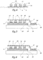
- Figures 4 to 6 illustrate welding phases, for securing the semiconductor circuit 2 with a added conductive organ.
- each ball 16 which is for example made of a tin-lead-silver alloy, so as to subject it to stud 14.
- this semiconductor circuit 2 receives, in known manner, a conductive layer 20 and a conductive track 22, this layer and this track being isolated from each other.
- the faces, opposite the substrate 18, are then covered with layer 20 and track 22 by means of welding films 24, 24 'made of the same alloy as the balls 16.
- This member 26 has a second end which is placed above the film of welding 24 'covering track 22.
- the primary and primary merger phases secondary can be implemented in a single step fusion.
- the welding balls 16 can be replaced by doses of a pasty welding material, which one delivers above each stud 14.
- FIGs 7 and 8 illustrate an electronic component of power obtained according to the process described with reference to Figures 1 to 6.
- This component comprises a substrate 68 on which are arranged a conductive layer 70, as well as two tracks conductive 72, this layer 70 and these tracks 72 being isolated from each other.
- a semiconductor power circuit 52 is added above layer 70, with interposition of a flat weld 80.
- Pads 64 which cover the face of the circuit 52 opposite to substrate 68, are subject to three bodies conductors 76, 76 ', 76' 'via bosses solder 78, 78 ', 78' '.
- the opposite ends conductive members 76 and 76 ' are subject to the track conductive 72, with interposition of planar welds 80 ′, while the member 76 '' is subject to runway 72 'by a 80 '' flat weld.
- the two conductive members 76 and 76 ' can be united in a single organ, dug from a notch for passage of the conductive member 76 '', intended for be isolated from the single conducting member thus formed.
- a cooling element to at least one of the sides of the electronic power component. So the face free of substrate 68 and / or the free face of the conductive members 76, 76 ', 76' 'can be brought into contact with such cooling element, of a type known per se.
- Figure 9 illustrates a first variant of the component power electronics of the invention.
- mechanical elements similar to those of FIGS. 7 and 8 have been assigned the same reference numbers, increased by 50.
- the component of Figure 9 includes a substrate lower 118, a conductive layer 120, a conductive track 122, as well as a semiconductor power circuit 102, whose studs 114 are connected to two conductive members 126, 126 '.
- One 126 of these is surmounted, opposite the circuit 102, by an upper substrate 118 ', while the other 126 ′ is connected to the conductive track 122, with interposition of a planar weld 130.
- Figure 10 illustrates an additional variant of production of a power electronic component according to the invention.
- elements similar to those Figures 7 and 8 have been assigned the same numbers reference, increased by 100.
- the component of FIG. 10 comprises a substrate 168, a conductive layer 170, two conductive tracks 172, 172 ' as well as two semiconductor circuits of power 152, 152.
- a first conductive member 176 is connected to several of the pads of the two semiconductor circuits 152, 152 ′ and also found reported above the conductive track 172.
- a second conductive member 176 ′ is connected to a stud 164 'of the second circuit 152', as well as to the track driver 172 '.
- This electronic power component allows to associate an insulated gate bipolar transistor, or IGBT, with a diode, mounted in anti-parallel.
- Layer 170 forms a collector, or cathode, the member 176 constitutes an emitter, or anode, while the conductive member 176 'forms a grid.
- the member 176 ' can extend more far as in Figure 9, in that it can be set relationship with at least one pad of the first semiconductor circuit 152. This arrangement makes it possible to form two IGBTs, placed in parallel.
- Figure 11 illustrates an additional variant of realization of the invention, figure in which the elements mechanical similar to those of FIGS. 7 and 8 have been assigned the same reference numbers, increased by 150.
- the lower substrate 218 supports a conductive layer 220, as well as four conductive tracks 222, 222 ', 223 and 223.
- Layer 220 supports a first semiconductor circuit 202, the studs of which are related to two conductive members 226, 226 '. One 226 of these organs is subject to conductive track 222, while the other 226 ' is subject to runway 222 '.
- An additional semiconductor circuit 232 is arranged on the conductive member 226 ', with the interposition of a weld plane 230, similar to that 80 described above.
- the studs 234 of circuit 232 are connected to two organs additional conductors 236, 236 ', one of which 236 is subject to runway 223, while the other 236 'is subject at runway 223 '.
- An upper substrate 218 ' is finally added on the face of the member 236 ′ opposite the circuit 232.
- FIG. 11 makes it possible to constitute two IGBT in series, all contacts of which are located on the lower substrate 218.
- the conductive member 226 ′, the conductive member 236 'and the conductive member 236 constitute respectively the collector, the emitter and the grid of this first IGBT.
- the conductive layer 220, the conductive member 226 'and the conductive member 226 constitute respectively the collector, the emitter and the grid from the second IGBT.
- the organs conductors 236, 236 ' are brought into contact with tracks conductive placed on the upper substrate 218 ', and not not on the lower substrate 218.
Abstract
Selon ce procédé, on dispose successivement sur un substrat (18) au moins une couche conductrice (20) et au moins un circuit semi-conducteur de puissance (2), et on rapporte, sur la face du circuit semi-conducteur (2) opposée à la couche conductrice (20), des plots métalliques (14) de connexion, par dépôt, par métallisation, d'un film métallique (12). On dispose ensuite au moins un élément de soudage (16) sur le ou chaque film (12) ainsi obtenu, on rapporte au moins un organe conducteur (26) sur le ou chaque élément de soudage (16), à l'opposé du film métallique (12), et on réalise une fusion du ou de chaque élément de soudage, de façon à assujettir le ou chaque organe conducteur (26) avec le ou chaque film métallique (12). <IMAGE>According to this method, there is successively disposed on a substrate (18) at least one conductive layer (20) and at least one power semiconductor circuit (2), and it is reported, on the face of the semiconductor circuit (2) opposite the conductive layer (20), metal studs (14) for connection, by deposition, by metallization, of a metallic film (12). Then there is at least one welding element (16) on the or each film (12) thus obtained, at least one conductive member (26) is attached to the or each welding element (16), opposite the film metallic (12), and a fusion of the or each welding element is carried out, so as to subject the or each conductive member (26) with the or each metallic film (12). <IMAGE>
Description
La présente invention concerne un procédé de fabrication d'un composant électronique de puissance, et un composant électronique de puissance ainsi obtenu.The present invention relates to a manufacturing process of a power electronic component, and a component power electronics thus obtained.
De manière habituelle, un composant électronique de puissance, qui est en particulier utilisé dans le domaine technique de la traction ferroviaire, comprend un substrat sur lequel sont rapportées plusieurs couches conductrices. Au moins un circuit semi-conducteur de puissance est disposé sur chacune de ces dernières, à savoir par exemple un transistor bipolaire à grille isolée, dit IGBT, ou bien encore une diode.Usually, an electronic component of power, which is particularly used in the field railway traction technique, includes a substrate on which are reported several conductive layers. At at least one semiconductor power circuit is disposed on each of these, for example a transistor bipolar with insulated grid, called IGBT, or even a diode.
Chaque circuit semi-conducteur est pourvu, sur sa face opposée à la couche conductrice précitée, de plots métalliques de connexion, sur lesquels sont soudés des fils d'aluminium présentant typiquement un diamètre de 380 à 500 microns. Chacun de ces fils est par ailleurs soudé sur une des couches conductrices recouvrant le substrat.Each semiconductor circuit is provided on its face opposite to the aforementioned conductive layer, of metal studs of connection, on which are welded aluminum wires typically having a diameter of 380 to 500 microns. Each of these wires is also welded to one of the layers conductive covering the substrate.
Ce composant électronique de puissance, de type connu, présente cependant certains inconvénients. En effet, les fils d'aluminium précités sont à l'origine de nombreux problèmes de fiabilité, liés aux contraintes mécaniques s'exerçant au niveau de la soudure entre ces fils et les plots de connexion correspondants.This power electronic component, of known type, has some drawbacks, however. Indeed, the sons aluminum aids cause many problems reliability, linked to the mechanical stresses level of solder between these wires and the connection pads correspondents.
Par ailleurs, ces fils sont à l'origine d'une inductance parasite susceptible de limiter les performances de l'ensemble du composant électronique de puissance. Enfin, ce dernier ne permet pas une évacuation optimale de la chaleur, puisque cette évacuation est réalisée sur une unique face de ce composant.Furthermore, these wires are the source of an inductance. parasite likely to limit the performance of the assembly of the power electronic component. Finally, the latter does not allow optimal heat dissipation, since this evacuation is carried out on a single face of this component.
Afin de résoudre, dans une certaine mesure, les problèmes précités, on a proposé des connexions de puissance ne faisant pas appel aux fils d'aluminium précités. A cet effet, il est mis en oeuvre un procédé de fabrication par contacts pressés, tel que celui décrit par exemple dans EP-A-0 784 342.In order to resolve, to some extent, the problems aforementioned, power connections have been proposed which do not not using the aforementioned aluminum wires. For this purpose, it is implemented a manufacturing process by pressing contacts, such as that described for example in EP-A-0 784 342.
Quand bien même ce procédé de réalisation apporte une solution satisfaisante en termes d'évacuation de la chaleur, il présente d'autres inconvénients, à savoir qu'il implique l'utilisation de mécanismes de pressage compliqués. Par ailleurs, il est peu commode à mettre en oeuvre, dans la mesure où il nécessite des circuits semi-conducteurs spécifiques.Even though this production process provides a satisfactory solution in terms of heat dissipation, it has other disadvantages, namely that it involves the use of complicated pressing mechanisms. Through elsewhere, it is inconvenient to implement, in the since it requires specific semiconductor circuits.
Afin de pallier l'ensemble de ces inconvénients, l'invention vise à proposer un procédé de fabrication d'un composant électronique de puissance, qui est simple et rapide à mettre en oeuvre et permet l'obtention d'un composant électronique robuste et garantissant une évacuation satisfaisante de la chaleur.In order to overcome all of these drawbacks, the invention aims to propose a method for manufacturing a power electronic component, which is simple and fast to implement and allows obtaining a component robust electronics ensuring satisfactory evacuation heat.
A cet effet, elle a pour objet un procédé de fabrication d'un composant électronique de puissance, dans lequel on dispose successivement sur un substrat, au moins une couche conductrice et au moins un circuit semi-conducteur de puissance, et dans lequel on rapporte, sur la face du circuit semi-conducteur opposée à la couche conductrice, des plots métalliques de connexion, caractérisé en ce que l'étape consistant à rapporter lesdits plots de connexion sur ladite face opposée du circuit semi-conducteur comprend une étape de dépôt, par métallisation, d'un film métallique, en ce qu'on dispose au moins un élément de soudage sur le ou chaque film ainsi obtenu, on rapporte au moins un organe conducteur sur le ou chaque élément de soudage, à l'opposé du film métallique, et en ce qu'on réalise une fusion du ou de chaque élément de soudage, de façon à assujettir le ou chaque organe conducteur avec le ou chaque film métallique.To this end, it relates to a manufacturing process of a power electronic component, in which successively has at least one layer on a substrate conductive and at least one semiconductor circuit of power, and in which we report, on the face of the circuit semiconductor opposite to the conductive layer, pads metallic connection, characterized in that the step consisting in bringing said connection pads onto said opposite side of the semiconductor circuit includes a step of deposition, by metallization, of a metallic film, in that has at least one welding element on the or each film thus obtained, at least one conductive member is reported on the or each welding element, opposite the metallic film, and in that we realize a fusion of or each element welding, so as to secure the or each member conductor with the or each metallic film.
L'invention permet de réaliser les objectifs précédemment mentionnés.The invention makes it possible to achieve the objectives previously mentioned.
En effet, le procédé de l'invention fait appel à des étapes de réalisation simples et aisées à mettre en oeuvre.In fact, the method of the invention calls upon simple and easy steps to implement.
Par ailleurs, le composant ainsi obtenu possède une fiabilité améliorée, dans la mesure où l'assujettissement par soudure permet de réduire, dans une mesure importante, les dilatations différentielles inhérentes à l'emploi antérieur des fils métalliques de connexion.Furthermore, the component thus obtained has a improved reliability, insofar as subjection by welding reduces, to a significant extent, the differential expansions inherent in previous use metallic connection wires.
En outre, le procédé de l'invention assure une évacuation satisfaisante de la chaleur, depuis les deux faces opposées de chaque circuit semi-conducteur.In addition, the method of the invention ensures evacuation satisfactory heat, from the two opposite sides of each semiconductor circuit.
Enfin, ce procédé est d'une flexibilité notable, dans la mesure où il permet la fabrication de composants électroniques de puissance à partir de circuits semi-conducteurs de natures différentes, sans modification substantielle des étapes de ce procédé.Finally, this process is remarkably flexible, in the since it allows the manufacture of electronic components power from natural semiconductor circuits different, without substantial modification of the stages of this process.
Selon une première variante de l'invention, on réalise l'étape de dépôt du film métallique directement sur une plaquette semi-conductrice vierge appartenant audit circuit semi-conducteur de puissance.According to a first variant of the invention, one realizes the step of depositing the metallic film directly on a blank semiconductor wafer belonging to said circuit power semiconductor.
Selon une seconde variante de l'invention, on réalise l'étape de dépôt dudit film métallique sur un organe de connexion préexistant dudit circuit semi-conducteur.According to a second variant of the invention, one realizes the step of depositing said metallic film on a pre-existing connection of said semiconductor circuit.
Un tel organe de connexion est par exemple constitué par une pellicule en aluminium, recouverte d'une couche d'oxyde d'aluminium. Ce mode de réalisation est avantageux, étant donné qu'il permet le traitement de composants classiques de l'art antérieur, voire une valorisation de composants usagés.Such a connection member is for example constituted by aluminum film, covered with an oxide layer aluminum. This embodiment is advantageous, being given that it allows the processing of conventional components of the prior art, or even a recovery of used components.
Selon une autre caractéristique de l'invention, le film métallique est constitué d'un alliage de titane-nickel.According to another characteristic of the invention, the film metal is made of a titanium-nickel alloy.
Selon une autre caractéristique de l'invention, on réalise l'étape de dépôt du film métallique, par métallisation au travers des ouvertures d'un masque. Ceci est avantageux en termes de commodité de fabrication, dans la mesure où ce masque peut être posé directement sur le circuit semi-conducteur que l'on désire revêtir.According to another characteristic of the invention, one performs the metal film deposition step, by metallization through the openings of a mask. This is advantageous in terms of manufacturing convenience, as far as this mask can be placed directly on the semiconductor circuit that we want to put on.
Selon une autre caractéristique de l'invention, chaque élément de soudage possède une dimension transversale supérieure à 0,5 mm et, de préférence, supérieure à 1 mm. On entend par dimension transversale, soit le diamètre de cet élément de soudage, soit sa plus grande largeur.According to another characteristic of the invention, each welding element has a transverse dimension greater than 0.5 mm and preferably greater than 1 mm. We by transverse dimension means the diameter of this welding element, or its greatest width.
Selon une première variante de l'invention, chaque élément de soudage est constitué par un élément préformé, notamment une bille. Ceci est avantageux, étant donné qu'il peut être aisément procédé à un stockage de ces éléments préformés. Par ailleurs, lors de là fabrication du composant de puissance, ces éléments préformés stockés peuvent être acheminés en direction de chaque film métallique, au travers des ouvertures du masque dont il est fait mention ci-dessus.According to a first variant of the invention, each welding element consists of a preformed element, including a ball. This is advantageous since it can easily be stored preformed. Furthermore, during the manufacture of the component of power, these stored preformed elements can be routed towards each metal film, through openings of the mask mentioned above.
Selon une seconde variante de l'invention, chaque élément de soudage est constitué par une dose de matière de soudage. According to a second variant of the invention, each element welding consists of a dose of welding material.
Selon une autre caractéristique de l'invention, chaque élément de soudage est réalisé en un alliage d'étain-plomb-argent.According to another characteristic of the invention, each soldering element is made of a tin-lead-silver alloy.
Selon un premier mode de réalisation de l'invention, l'étape de fusion du ou de chaque élément de soudage comporte une phase primaire de fusion, permettant d'assujettir chaque élément de soudage sur le film métallique, on rapporte ensuite le ou chaque organe conducteur sur le ou chaque élément de soudage après ladite phase primaire, et il est prévu une phase secondaire de fusion, permettant d'assujettir chaque élément de soudage avec un organe conducteur correspondant. Ce mode de réalisation permet, une fois la phase de fusion primaire mise en oeuvre, de positionner de façon stable chaque élément de soudage sur le plot métallique qu'il recouvre.According to a first embodiment of the invention, the step of melting the or each welding element comprises a primary merger phase, allowing each welding element on the metallic film, we then report the or each conductive member on the or each element of welding after said primary phase, and a phase is provided secondary fusion, allowing to subject each element welding with a corresponding conductive member. This mode Once the primary fusion phase has been completed, implementation, to position each element stably welding on the metal stud it covers.
Selon un second mode de réalisation de l'invention, on rapporte chaque organe conducteur sur chaque élément de soudage, puis on réalise ladite fusion de cet élément de soudage en une seule étape. Ce mode de réalisation est avantageux en termes de rapidité et de simplicité.According to a second embodiment of the invention, we reports each conductive organ on each element of welding, then said fusion of this element of one step welding. This embodiment is advantageous in terms of speed and simplicity.
Selon une autre caractéristique avantageuse de l'invention, on assujettit chaque circuit semi-conducteur de puissance sur une couche conductrice correspondante en intercalant, entre ce circuit et cette couche, un film de soudage, puis en opérant une fusion dudit film, ce film et chaque élément de soudage étant réalisés dans le même matériau. Cette mesure garantit une grande commodité de réalisation, et induit de faibles coûts de fabrication.According to another advantageous characteristic of the invention, each semiconductor circuit is subject to power on a corresponding conductive layer in intercalating, between this circuit and this layer, a film of welding, then by operating a fusion of said film, this film and each welding element being made in the same material. This measure guarantees great convenience in realization, and induces low manufacturing costs.
Selon une caractéristique particulièrement avantageuse de l'invention, on réalise la fusion, d'une part dudit film de soudage et, d'autre part, de chaque élément de soudage, en une unique étape. Cette fusion est par exemple réalisée dans un four, dont la température est comprise en 180 et 300°C.According to a particularly advantageous characteristic of the invention, the fusion is carried out, on the one hand of said film of welding and, on the other hand, of each welding element, in a single step. This merger is for example carried out in an oven, the temperature of which is between 180 and 300 ° C.
Cette mesure assure une diminution substantielle du temps de fabrication du composant électronique. En effet, on assujettit en une unique étape, d'une part, chaque circuit semi-conducteur sur une couche conductrice correspondante et, d'autre part, chaque organe conducteur sur le film métallique dont est pourvu ce circuit semi-conducteur. This measure ensures a substantial reduction in time manufacturing the electronic component. Indeed, we subjects in a single step, on the one hand, each circuit semiconductor on a corresponding conductive layer and, on the other hand, each conductive member on the metallic film with which this semiconductor circuit is provided.
L'invention a également pour objet un composant électronique de puissance, comprenant un substrat, au moins une couche conductrice supportée par ce substrat, et au moins un premier circuit semi-conducteur de puissance disposé sur ladite couche conductrice et comportant des plots métalliques de connexion assujettis, par leur face opposée au substrat, à au moins un organe conducteur, ledit composant étant réalisé selon le procédé tel que défini ci-dessus.The invention also relates to an electronic component power, comprising a substrate, at least one conductive layer supported by this substrate, and at least one first semiconductor power circuit arranged on said conductive layer and comprising metal pads connection subject, by their face opposite to the substrate, at least one conductive member, said component being produced according to the method as defined above.
Selon d'autres caractéristiques de l'invention :
- ce composant comporte au moins deux organes conducteurs isolés entre eux ;
- ces deux organes conducteurs comprennent un émetteur et une grille, dont l'un au moins est commun à plusieurs circuits semi-conducteurs disposés sur ledit substrat ;
- ce composant comporte en outre au moins un circuit semi-conducteur supplémentaire, rapporté sur le ou chaque organe conducteur à l'opposé dudit premier circuit semi-conducteur.
- this component comprises at least two conductive members isolated from each other;
- these two conductive members comprise an emitter and a gate, at least one of which is common to several semiconductor circuits arranged on said substrate;
- this component further comprises at least one additional semiconductor circuit, attached to the or each conductive member opposite said first semiconductor circuit.
L'invention va être décrite ci-dessous, en référence aux dessins annexés, donnés uniquement à titre d'exemples non limitatifs et dans lesquels :
- les figures 1 à 3 sont des vues, respectivement de côté et de dessus, illustrant trois phases successives de dépôt d'un film métallique, par métallisation, sur un circuit semi-conducteur de puissance ;
- les figures 4 à 6 sont des vues de côté illustrant trois phases successives de l'assujettissement d'un organe conducteur sur le circuit semi-conducteur de puissance des figures 1 à 3 ;
- les figures 7 et 8 sont des vues, respectivement de côté et de dessus, illustrant un premier mode de réalisation d'un composant électronique de puissance obtenu selon l'invention ; et
- les figures 9 à 11 sont des vues de côté illustrant trois variantes de réalisation d'un composant électronique de puissance obtenu selon l'invention.
- Figures 1 to 3 are views, respectively from the side and from above, illustrating three successive phases of deposition of a metallic film, by metallization, on a power semiconductor circuit;
- Figures 4 to 6 are side views illustrating three successive phases of the securing of a conductive member on the power semiconductor circuit of Figures 1 to 3;
- Figures 7 and 8 are views, respectively from the side and from above, illustrating a first embodiment of a power electronic component obtained according to the invention; and
- Figures 9 to 11 are side views illustrating three alternative embodiments of a power electronic component obtained according to the invention.
Les figures 1 à 3 illustrent une étape de métallisation
d'un circuit semi-conducteur de puissance. Ce dernier, désigné
dans son ensemble par la référence 2, comprend une plaquette
semi-conductrice 4 surmontée par plusieurs organes de
connexion préexistants, à savoir des pellicules 6 visibles à
la figure 1. Ces pellicules, réalisées par exemple en aluminium,
sont recouvertes d'une couche d'oxyde non représentée,
sur leur face opposée à la plaquette 4. Cette couche est
formée lors de l'oxydation des pellicules en aluminium, dans
l'air ambiant.Figures 1 to 3 illustrate a metallization step
a semiconductor power circuit. The latter, designated
as a whole by
L'étape de métallisation consiste tout d'abord à
rapporter un masque 8, pourvu d'ouvertures 10, à proximité des
pellicules 6. Puis, on procède au revêtement de ces pellicules
6, au travers des ouvertures 10 précitées. Cette métallisation
est effectuée de façon connue, par exemple par évaporation
thermique, ou bien encore par évaporation par faisceaux
d'électrons ou analogue. Le métal mis en oeuvre est par
exemple un alliage titane-nickel.The metallization step consists first of all in
add a
Cette étape de revêtement conduit à la formation d'un
film métallique 12, s'étendant au-dessus de la couche d'oxyde
recouvrant chaque pellicule. Cette pellicule 6 et ce film 12
forment un plot métallique de connexion, désigné dans son
ensemble par la référence 14.This coating step leads to the formation of a
A titre de variante, on peut déposer le masque 8
directement à la surface de la plaquette 4, de sorte que les
ouvertures 10 débouchent à la surface libre des pellicules 6.
On peut également effectuer l'étape de métallisation directement
sur une plaquette semi-conductrice vierge, analogue à
celle 4 des figures 1 à 3.Alternatively,
Les figures 4 à 6 illustrent des phases de soudage,
permettant d'assujettir le circuit semi-conducteur 2 avec un
organe conducteur rapporté.Figures 4 to 6 illustrate welding phases,
for securing the
Dans un premier temps, comme l'illustre la figure 4, on
rapporte un élément de soudage 16, qui est une bille, sur
chaque plot 14 formé selon l'étape illustrée aux figures 2 et
3. Ces billes 16 sont avantageusement acheminées en direction
des plots 14, au travers des ouvertures 10 du masque 8, non
représenté sur cette figure 4.First, as illustrated in Figure 4, we
attaches a
On procède ensuite à une fusion primaire de chaque bille
16, qui est par exemple réalisée en un alliage d'étain-plomb-argent,
de façon à l'assujettir au plot 14.We then proceed to a primary fusion of each
Puis, comme l'illustre la figure 5, il s'agit de
rapporter ce circuit semi-conducteur 2 sur un substrat 18. Ce
dernier reçoit, de façon connue, une couche conductrice 20 et
une piste conductrice 22, cette couche et cette piste étant
isolées entre elles.Then, as illustrated in figure 5, it is a question of
report this
On recouvre alors les faces, opposées au substrat 18, de
la couche 20 et de la piste 22 au moyen de films de soudage
24, 24' réalisés dans le même alliage que les billes 16. On
dispose alors le circuit 2, surmonté des billes 16, sur le
film de soudage 24, ainsi qu'un organe conducteur 26 sur la
face des billes 16 opposée au circuit 2. Cet organe 26 possède
une seconde extrémité que l'on place au-dessus du film de
soudage 24' recouvrant la piste 22.The faces, opposite the
Puis, comme le montre la figure 6, on procède à un
chauffage des différents éléments illustrés à la figure 5, de
manière à induire la fusion simultanée des billes 16, ainsi
que des films 24, 24'. Ceci conduit à la formation d'une
première série de soudures 28, de forme à peu près tubulaire,
permettant d'assujettir les plots 14 avec l'organe conducteur
26. Le chauffage précité provoque également la formation de
soudures planes 30, 30' reliant, d'une part, la couche conductrice
20 au circuit semi-conducteur 2 et, d'autre part, la
piste conductrice 22 à la seconde extrémité de l'organe
conducteur 26.Then, as shown in Figure 6, we proceed to a
heating of the various elements illustrated in FIG. 5, of
so as to induce the simultaneous fusion of the
A titre de variante, les phases de fusions primaire et
secondaire, illustrées respectivement aux figures 5 et 6,
peuvent être mises en oeuvre au cours d'une unique étape de
fusion. Par ailleurs, les billes de soudage 16 peuvent être
remplacées par des doses d'une matière pâteuse de soudage, que
l'on délivre au-dessus de chaque plot 14.Alternatively, the primary and primary merger phases
secondary, illustrated respectively in FIGS. 5 and 6,
can be implemented in a single step
fusion. Furthermore, the
Les figures 7 et 8 illustrent un composant électronique de puissance obtenu selon le procédé décrit en référence aux figures 1 à 6.Figures 7 and 8 illustrate an electronic component of power obtained according to the process described with reference to Figures 1 to 6.
Ce composant comprend un substrat 68 sur lequel sont
disposées une couche conductrice 70, ainsi que deux pistes
conductrices 72, cette couche 70 et ces pistes 72 étant
isolées entre elles. Un circuit semi-conducteur de puissance
52 est rapporté au-dessus de la couche 70, avec interposition
d'une soudure plane 80.This component comprises a
Des plots 64, qui recouvrent la face du circuit 52
opposée au substrat 68, sont assujettis à trois organes
conducteurs 76, 76', 76'' par l'intermédiaire de bossages de
soudure 78, 78', 78''. Par ailleurs, les extrémités opposées
des organes conducteurs 76 et 76' sont assujetties à la piste
conductrice 72, avec interposition de soudures planes 80',
alors que l'organe 76'' est assujetti à la piste 72' par une
soudure plane 80''.
A titre de variante, les deux organes conducteurs 76 et
76' peuvent être réunis en un unique organe, creusé d'une
échancrure de passage de l'organe conducteur 76'', destiné à
être isolé de l'organe conducteur unique ainsi formé.As a variant, the two
A titre de variante, il est également possible de
rapporter un élément de refroidissement sur au moins l'une des
faces du composant électronique de puissance. Ainsi, la face
libre du substrat 68 et/ou la face libre des organes conducteurs
76, 76', 76'' peut être mise en contact avec un tel
élément de refroidissement, de type connu en soi.Alternatively, it is also possible to
add a cooling element to at least one of the
sides of the electronic power component. So the face
free of
La figure 9 illustre une première variante du composant électronique de puissance de l'invention. Sur cette figure, les éléments mécaniques analogues à ceux des figures 7 et 8 ont été affectés des mêmes numéros de référence, augmentés de 50.Figure 9 illustrates a first variant of the component power electronics of the invention. In this figure, mechanical elements similar to those of FIGS. 7 and 8 have been assigned the same reference numbers, increased by 50.
Le composant de la figure 9 comprend un substrat
inférieur 118, une couche conductrice 120, une piste conductrice
122, ainsi qu'un circuit semi-conducteur de puissance
102, dont les plots 114 sont reliés à deux organes conducteurs
126, 126'. L'un 126 de ceux-ci est surmonté, à l'opposé du
circuit 102, par un substrat supérieur 118', alors que l'autre
126' est relié à la piste conductrice 122, avec interposition
d'une soudure plane 130.The component of Figure 9 includes a substrate
lower 118, a
La figure 10 illustre une variante supplémentaire de réalisation d'un composant électronique de puissance selon l'invention. Sur cette figure, les éléments analogues à ceux des figures 7 et 8 ont été affectés des mêmes numéros de référence, augmentés de 100.Figure 10 illustrates an additional variant of production of a power electronic component according to the invention. In this figure, elements similar to those Figures 7 and 8 have been assigned the same numbers reference, increased by 100.
Le composant de la figure 10 comprend un substrat 168,
une couche conductrice 170, deux pistes conductrices 172, 172'
ainsi que deux circuits semi-conducteurs de puissance 152,
152'. Un premier organe conducteur 176 est relié à plusieurs
des plots des deux circuits semi-conducteur 152, 152' et se
trouve également rapporté au-dessus de la piste conductrice
172. Par ailleurs, un second organe conducteur 176' est relié
à un plot 164' du second circuit 152', ainsi qu'à la piste
conductrice 172'.The component of FIG. 10 comprises a
Ce composant électronique de puissance permet d'associer
un transistor bipolaire à grille isolée, ou IGBT, avec une
diode, montés en anti-parallèle. La couche 170 forme un
collecteur, ou cathode, l'organe 176 constitue un émetteur,
ou anode, alors que l'organe conducteur 176' forme une grille.This electronic power component allows to associate
an insulated gate bipolar transistor, or IGBT, with a
diode, mounted in anti-parallel.
A titre de variante, l'organe 176' peut s'étendre plus
loin que sur la figure 9, en ce sens qu'il peut être mis en
relation avec au moins un plot du premier circuit semi-conducteur
152. Cet agencement permet de former deux IGBT,
placés en parallèle.Alternatively, the member 176 'can extend more
far as in Figure 9, in that it can be set
relationship with at least one pad of the
La figure 11 illustre une variante supplémentaire de réalisation de l'invention, figure sur laquelle les éléments mécaniques analogues à ceux des figures 7 et 8 ont été affectés des mêmes numéros de référence, augmentés de 150.Figure 11 illustrates an additional variant of realization of the invention, figure in which the elements mechanical similar to those of FIGS. 7 and 8 have been assigned the same reference numbers, increased by 150.
Le substrat inférieur 218 supporte une couche conductrice
220, ainsi que quatre pistes conductrices 222, 222', 223 et
223'. La couche 220 supporte un premier circuit semi-conducteur
202, dont les plots sont mis en relation avec deux
organes conducteurs 226, 226'. L'un 226 de ces organes est
assujetti à la piste conductrice 222, alors que l'autre 226'
est assujetti à la piste 222'.The
Un circuit semi-conducteur supplémentaire 232 est disposé
sur l'organe conducteur 226', avec interposition d'une soudure
plane 230, analogue à.celle 80 décrite ci-dessus. Les plots
234 du circuit 232 sont mis en relation avec deux organes
conducteurs supplémentaires 236, 236', dont l'un 236 est
assujetti à la piste 223, alors que l'autre 236' est assujetti
à la piste 223'. Un substrat supérieur 218' est enfin rapporté
sur la face de l'organe 236' opposée au circuit 232.An
L'agencement de la figure 11 permet de constituer deux
IGBT en série, dont tous les contacts sont situés sur le
substrat inférieur 218. Ainsi, l'organe conducteur 226',
l'organe conducteur 236' et l'organe conducteur 236 constituent
respectivement le collecteur, l'émetteur et la grille
de ce premier IGBT. Par ailleurs, la couche conductrice 220,
l'organe conducteur 226' et l'organe conducteur 226 constituent
respectivement le collecteur, l'émetteur et la grille
du second IGBT.The arrangement of FIG. 11 makes it possible to constitute two
IGBT in series, all contacts of which are located on the
A titre de variante, on peut prévoir que les organes
conducteurs 236, 236' soient mis en contact avec des pistes
conductrices placées sur le substrat supérieur 218', et non
pas sur le substrat inférieur 218.Alternatively, it can be provided that the
Claims (17)
Applications Claiming Priority (2)
| Application Number | Priority Date | Filing Date | Title |
|---|---|---|---|
| FR0008931 | 2000-07-07 | ||
| FR0008931A FR2811475B1 (en) | 2000-07-07 | 2000-07-07 | METHOD FOR MANUFACTURING AN ELECTRONIC POWER COMPONENT, AND ELECTRONIC POWER COMPONENT THUS OBTAINED |
Publications (1)
| Publication Number | Publication Date |
|---|---|
| EP1170794A1 true EP1170794A1 (en) | 2002-01-09 |
Family
ID=8852273
Family Applications (1)
| Application Number | Title | Priority Date | Filing Date |
|---|---|---|---|
| EP01401764A Ceased EP1170794A1 (en) | 2000-07-07 | 2001-07-02 | Method of fabricating a power electronic component and power electronic component obtained thereby |
Country Status (5)
| Country | Link |
|---|---|
| US (1) | US6589859B2 (en) |
| EP (1) | EP1170794A1 (en) |
| JP (1) | JP2002093977A (en) |
| CA (1) | CA2352513A1 (en) |
| FR (1) | FR2811475B1 (en) |
Cited By (1)
| Publication number | Priority date | Publication date | Assignee | Title |
|---|---|---|---|---|
| WO2005101504A1 (en) * | 2004-04-19 | 2005-10-27 | Siemens Aktiengesellschaft | Power module |
Families Citing this family (16)
| Publication number | Priority date | Publication date | Assignee | Title |
|---|---|---|---|---|
| JP4136845B2 (en) * | 2002-08-30 | 2008-08-20 | 富士電機ホールディングス株式会社 | Manufacturing method of semiconductor module |
| US7614998B2 (en) * | 2003-02-24 | 2009-11-10 | Yossi Gross | Fully-implantable cardiac recovery system |
| JP4491244B2 (en) * | 2004-01-07 | 2010-06-30 | 三菱電機株式会社 | Power semiconductor device |
| US20070152025A1 (en) * | 2004-03-02 | 2007-07-05 | Fuji Electric Holdings Co., Ltd. | Electronic part mounting method |
| JP4508189B2 (en) * | 2004-03-02 | 2010-07-21 | 富士電機ホールディングス株式会社 | Manufacturing method of semiconductor module |
| JP4378239B2 (en) * | 2004-07-29 | 2009-12-02 | 株式会社日立製作所 | A semiconductor device, a power conversion device using the semiconductor device, and a hybrid vehicle using the power conversion device. |
| JP4566678B2 (en) * | 2004-10-04 | 2010-10-20 | 日立オートモティブシステムズ株式会社 | Power module |
| JP4478049B2 (en) * | 2005-03-15 | 2010-06-09 | 三菱電機株式会社 | Semiconductor device |
| US7915081B2 (en) * | 2006-03-31 | 2011-03-29 | Intel Corporation | Flexible interconnect pattern on semiconductor package |
| JP4564937B2 (en) | 2006-04-27 | 2010-10-20 | 日立オートモティブシステムズ株式会社 | Electric circuit device, electric circuit module, and power conversion device |
| GB2452594B (en) * | 2007-08-20 | 2012-04-25 | Champion Aerospace Inc | Switching assembly for an aircraft ignition system |
| EP2239769B1 (en) * | 2008-01-25 | 2019-11-06 | Consejo Superior De Investigaciones Científicas | Self-aligned metal mask assembly for selectively depositing thin films on microelectronic substrates and devices, and method of use |
| FR2959350B1 (en) * | 2010-04-26 | 2012-08-31 | Commissariat Energie Atomique | METHOD FOR MANUFACTURING A MICROELECTRONIC DEVICE AND MICROELECTRONIC DEVICE SO MANUFACTURED |
| WO2018211685A1 (en) | 2017-05-19 | 2018-11-22 | 新電元工業株式会社 | Electronic module |
| WO2018211680A1 (en) | 2017-05-19 | 2018-11-22 | 新電元工業株式会社 | Electronic module |
| US11776937B2 (en) | 2018-07-04 | 2023-10-03 | Shindengen Electric Manufacturing Co., Ltd. | Electronic module |
Citations (7)
| Publication number | Priority date | Publication date | Assignee | Title |
|---|---|---|---|---|
| US3838984A (en) * | 1973-04-16 | 1974-10-01 | Sperry Rand Corp | Flexible carrier and interconnect for uncased ic chips |
| US4811081A (en) * | 1987-03-23 | 1989-03-07 | Motorola, Inc. | Semiconductor die bonding with conductive adhesive |
| US4967261A (en) * | 1987-07-30 | 1990-10-30 | Mitsubishi Denki Kabushiki Kaisha | Tape carrier for assembling an IC chip on a substrate |
| US4977441A (en) * | 1985-12-25 | 1990-12-11 | Hitachi, Ltd. | Semiconductor device and tape carrier |
| US5277756A (en) * | 1990-07-02 | 1994-01-11 | Digital Equipment Corporation | Post fabrication processing of semiconductor chips |
| EP0966038A2 (en) * | 1998-06-15 | 1999-12-22 | Ford Motor Company | Bonding of semiconductor power devices |
| FR2787920A1 (en) * | 1998-12-28 | 2000-06-30 | Alstom | METHOD FOR ASSEMBLING A CHIP TO A CIRCUIT MEMBER BY BRAZING |
Family Cites Families (16)
| Publication number | Priority date | Publication date | Assignee | Title |
|---|---|---|---|---|
| JPS5264285A (en) * | 1975-11-21 | 1977-05-27 | Hitachi Ltd | Production of compositemetal layer of integrated circuit device |
| US5001545A (en) * | 1988-09-09 | 1991-03-19 | Motorola, Inc. | Formed top contact for non-flat semiconductor devices |
| US5016082A (en) * | 1988-09-16 | 1991-05-14 | Delco Electronics Corporation | Integrated circuit interconnect design |
| JPH06104374A (en) * | 1991-01-04 | 1994-04-15 | Internatl Business Mach Corp <Ibm> | Electronic-circuit package as well as apparatus and method for molding and working of its conductor |
| JP3540864B2 (en) * | 1995-04-27 | 2004-07-07 | 新日本製鐵株式会社 | Method of forming fine bumps |
| JPH0936186A (en) * | 1995-07-24 | 1997-02-07 | Hitachi Ltd | Power semiconductor module and its mounting method |
| JP3387282B2 (en) * | 1995-08-03 | 2003-03-17 | 日産自動車株式会社 | Semiconductor device structure and method of manufacturing the same |
| JPH09129647A (en) * | 1995-10-27 | 1997-05-16 | Toshiba Corp | Semiconductor element |
| US6171888B1 (en) * | 1996-03-08 | 2001-01-09 | Lsi Logic Corp. | Multi-layer tab tape having distinct signal, power and ground planes, semiconductor device assembly employing same, apparatus for and method of assembling same |
| US5994222A (en) * | 1996-06-24 | 1999-11-30 | Tessera, Inc | Method of making chip mountings and assemblies |
| US5872403A (en) * | 1997-01-02 | 1999-02-16 | Lucent Technologies, Inc. | Package for a power semiconductor die and power supply employing the same |
| JPH10223683A (en) * | 1997-02-04 | 1998-08-21 | Hitachi Ltd | Semiconductor module |
| US6396127B1 (en) * | 1998-09-25 | 2002-05-28 | International Rectifier Corporation | Semiconductor package |
| US6221750B1 (en) * | 1998-10-28 | 2001-04-24 | Tessera, Inc. | Fabrication of deformable leads of microelectronic elements |
| US6319755B1 (en) * | 1999-12-01 | 2001-11-20 | Amkor Technology, Inc. | Conductive strap attachment process that allows electrical connector between an integrated circuit die and leadframe |
| DE202012103424U1 (en) * | 2011-12-09 | 2013-03-11 | Epiphanostics GmbH | Enossal single-tooth implant |
-
2000
- 2000-07-07 FR FR0008931A patent/FR2811475B1/en not_active Expired - Lifetime
-
2001
- 2001-07-02 EP EP01401764A patent/EP1170794A1/en not_active Ceased
- 2001-07-05 JP JP2001204556A patent/JP2002093977A/en active Pending
- 2001-07-06 US US09/899,078 patent/US6589859B2/en not_active Expired - Lifetime
- 2001-07-06 CA CA002352513A patent/CA2352513A1/en not_active Abandoned
Patent Citations (7)
| Publication number | Priority date | Publication date | Assignee | Title |
|---|---|---|---|---|
| US3838984A (en) * | 1973-04-16 | 1974-10-01 | Sperry Rand Corp | Flexible carrier and interconnect for uncased ic chips |
| US4977441A (en) * | 1985-12-25 | 1990-12-11 | Hitachi, Ltd. | Semiconductor device and tape carrier |
| US4811081A (en) * | 1987-03-23 | 1989-03-07 | Motorola, Inc. | Semiconductor die bonding with conductive adhesive |
| US4967261A (en) * | 1987-07-30 | 1990-10-30 | Mitsubishi Denki Kabushiki Kaisha | Tape carrier for assembling an IC chip on a substrate |
| US5277756A (en) * | 1990-07-02 | 1994-01-11 | Digital Equipment Corporation | Post fabrication processing of semiconductor chips |
| EP0966038A2 (en) * | 1998-06-15 | 1999-12-22 | Ford Motor Company | Bonding of semiconductor power devices |
| FR2787920A1 (en) * | 1998-12-28 | 2000-06-30 | Alstom | METHOD FOR ASSEMBLING A CHIP TO A CIRCUIT MEMBER BY BRAZING |
Non-Patent Citations (3)
| Title |
|---|
| LIU ET AL: "Packaging of integrated power electronics modules using flip-chip technology", IEEE, 6 February 2000 (2000-02-06), pages 290 - 296, XP010371710 * |
| PAULASTO ET AL: "Reliability of flip chip die attach in multichip mechatronic power module", IEEE, 18 June 2000 (2000-06-18), pages 93 - 100, XP010506356 * |
| WIEGELE ET AL: "Reliability and process characterization of electroless Nickel-Gold/Solder flip chip interconnect technology", ELECTRONIC COMPONENTS AND TECHNOLOGY CONFERENCE, 25 May 1998 (1998-05-25), pages 861 - 866, XP010283849 * |
Cited By (2)
| Publication number | Priority date | Publication date | Assignee | Title |
|---|---|---|---|---|
| WO2005101504A1 (en) * | 2004-04-19 | 2005-10-27 | Siemens Aktiengesellschaft | Power module |
| US7466020B2 (en) | 2004-04-19 | 2008-12-16 | Siemens Aktiengesellschaft | Power module |
Also Published As
| Publication number | Publication date |
|---|---|
| US6589859B2 (en) | 2003-07-08 |
| US20020006685A1 (en) | 2002-01-17 |
| FR2811475B1 (en) | 2002-08-23 |
| JP2002093977A (en) | 2002-03-29 |
| CA2352513A1 (en) | 2002-01-07 |
| FR2811475A1 (en) | 2002-01-11 |
Similar Documents
| Publication | Publication Date | Title |
|---|---|---|
| EP1170794A1 (en) | Method of fabricating a power electronic component and power electronic component obtained thereby | |
| CA2290801C (en) | Electronic power device | |
| EP1005083B1 (en) | High-power electronic device comprising cooling system | |
| FR2641646A1 (en) | SOLAR CELL AND MANUFACTURING METHOD THEREOF | |
| FR3018953A1 (en) | INTEGRATED CIRCUIT CHIP MOUNTED ON AN INTERPOSER | |
| EP0217471B1 (en) | Semiconductor power device for surface mounting | |
| CN103943518B (en) | Method for manufacturing the connection firmly engaged and electrical connection | |
| FR2541824A1 (en) | SEMICONDUCTOR POWER DEVICE CONSISTING OF A MULTIPLICITY OF SIMILAR ELEMENTS MOUNTED IN PARALLEL | |
| FR2786657A1 (en) | Power electronic component with cooling surfaces includes dual cooling panels forming sandwich to enclose semiconductor element | |
| EP0446125B1 (en) | Power semiconductor device | |
| EP0734066B1 (en) | Electronic power module | |
| EP0117804B1 (en) | Manufacturing method of a microwave cavity, and cavity obtained thereby | |
| FR2790905A1 (en) | POWER ELECTRICAL COMPONENT MOUNTED BY BRAZING ON A SUPPORT AND ASSEMBLY METHOD THEREFOR | |
| EP0619616B1 (en) | Apparatus exploiting the Peltier effect to detect the risk of condensation on a surface which borders a volume of humid air | |
| WO2006122692A2 (en) | Laser device formed by a stack of laser diodes | |
| EP0863389A1 (en) | Thermoelectric sensor | |
| EP0549405B1 (en) | Method of wiring a laser array | |
| FR2786658A1 (en) | Composite structure for electronic power components including cooling system, comprising channels for passage of coolant in lower conductor or semiconductor layer | |
| FR2517471A1 (en) | PRESS BOX MOUNTING OF POWER COMPONENTS WITH BRANCHED ELECTRODES STRUCTURE | |
| FR2523397A1 (en) | Mounting method for chip carriers on substrate - uses intermediate ceramic carrier plate which is glued to substrate and allows differential thermal strains | |
| CA1315415C (en) | Process for mounting a semi-conductor on a thermal dissipation and electrical connection support | |
| FR2574222A1 (en) | Method of fabricating a substrate for a hybrid circuit containing weakly resistive connections | |
| FR2747866A1 (en) | ELECTRONIC ASSEMBLY INCLUDING AN ELECTRONIC UNIT CONNECTED TO A COIL | |
| FR2653595A1 (en) | Electronic circuit inter-connection grid | |
| FR2787920A1 (en) | METHOD FOR ASSEMBLING A CHIP TO A CIRCUIT MEMBER BY BRAZING |
Legal Events
| Date | Code | Title | Description |
|---|---|---|---|
| PUAI | Public reference made under article 153(3) epc to a published international application that has entered the european phase |
Free format text: ORIGINAL CODE: 0009012 |
|
| AK | Designated contracting states |
Kind code of ref document: A1 Designated state(s): AT BE CH CY DE DK ES FI FR GB GR IE IT LI LU MC NL PT SE TR |
|
| AX | Request for extension of the european patent |
Free format text: AL;LT;LV;MK;RO;SI |
|
| 17P | Request for examination filed |
Effective date: 20020604 |
|
| AKX | Designation fees paid |
Free format text: AT BE CH CY DE DK ES FI FR GB GR IE IT LI LU MC NL PT SE TR |
|
| RAP1 | Party data changed (applicant data changed or rights of an application transferred) |
Owner name: ALSTOM |
|
| 17Q | First examination report despatched |
Effective date: 20050222 |
|
| STAA | Information on the status of an ep patent application or granted ep patent |
Free format text: STATUS: THE APPLICATION HAS BEEN REFUSED |
|
| 18R | Application refused |
Effective date: 20070414 |