EP1122795A2 - High dielectric constant gate oxides for silicon-based devices - Google Patents
High dielectric constant gate oxides for silicon-based devices Download PDFInfo
- Publication number
- EP1122795A2 EP1122795A2 EP01300746A EP01300746A EP1122795A2 EP 1122795 A2 EP1122795 A2 EP 1122795A2 EP 01300746 A EP01300746 A EP 01300746A EP 01300746 A EP01300746 A EP 01300746A EP 1122795 A2 EP1122795 A2 EP 1122795A2
- Authority
- EP
- European Patent Office
- Prior art keywords
- rare earth
- semiconductor device
- earth oxide
- silicon
- major surface
- Prior art date
- Legal status (The legal status is an assumption and is not a legal conclusion. Google has not performed a legal analysis and makes no representation as to the accuracy of the status listed.)
- Withdrawn
Links
- XUIMIQQOPSSXEZ-UHFFFAOYSA-N Silicon Chemical compound [Si] XUIMIQQOPSSXEZ-UHFFFAOYSA-N 0.000 title claims abstract description 50
- 229910052710 silicon Inorganic materials 0.000 title claims abstract description 44
- 239000010703 silicon Substances 0.000 title claims abstract description 44
- CMIHHWBVHJVIGI-UHFFFAOYSA-N gadolinium(III) oxide Inorganic materials [O-2].[O-2].[O-2].[Gd+3].[Gd+3] CMIHHWBVHJVIGI-UHFFFAOYSA-N 0.000 claims abstract description 46
- VYPSYNLAJGMNEJ-UHFFFAOYSA-N Silicium dioxide Chemical compound O=[Si]=O VYPSYNLAJGMNEJ-UHFFFAOYSA-N 0.000 claims abstract description 40
- 239000000758 substrate Substances 0.000 claims abstract description 34
- 229910001404 rare earth metal oxide Inorganic materials 0.000 claims abstract description 23
- 229910052681 coesite Inorganic materials 0.000 claims abstract description 20
- 229910052906 cristobalite Inorganic materials 0.000 claims abstract description 20
- 239000000377 silicon dioxide Substances 0.000 claims abstract description 20
- 229910052682 stishovite Inorganic materials 0.000 claims abstract description 20
- 229910052905 tridymite Inorganic materials 0.000 claims abstract description 20
- QVGXLLKOCUKJST-UHFFFAOYSA-N atomic oxygen Chemical compound [O] QVGXLLKOCUKJST-UHFFFAOYSA-N 0.000 claims abstract description 9
- 239000001301 oxygen Substances 0.000 claims abstract description 9
- 229910052760 oxygen Inorganic materials 0.000 claims abstract description 9
- GEYXPJBPASPPLI-UHFFFAOYSA-N manganese(III) oxide Inorganic materials O=[Mn]O[Mn]=O GEYXPJBPASPPLI-UHFFFAOYSA-N 0.000 claims abstract description 5
- 238000000034 method Methods 0.000 claims description 22
- 239000004065 semiconductor Substances 0.000 claims description 18
- 239000007789 gas Substances 0.000 claims description 10
- 239000000919 ceramic Substances 0.000 claims description 9
- 230000001747 exhibiting effect Effects 0.000 claims description 6
- 239000012535 impurity Substances 0.000 claims description 4
- 238000010894 electron beam technology Methods 0.000 claims description 3
- UFHFLCQGNIYNRP-UHFFFAOYSA-N Hydrogen Chemical compound [H][H] UFHFLCQGNIYNRP-UHFFFAOYSA-N 0.000 claims description 2
- 238000000137 annealing Methods 0.000 claims description 2
- 239000001257 hydrogen Substances 0.000 claims description 2
- 229910052739 hydrogen Inorganic materials 0.000 claims description 2
- GNFTZDOKVXKIBK-UHFFFAOYSA-N 3-(2-methoxyethoxy)benzohydrazide Chemical compound COCCOC1=CC=CC(C(=O)NN)=C1 GNFTZDOKVXKIBK-UHFFFAOYSA-N 0.000 claims 3
- 238000004140 cleaning Methods 0.000 claims 2
- 238000001704 evaporation Methods 0.000 claims 2
- FGUUSXIOTUKUDN-IBGZPJMESA-N C1(=CC=CC=C1)N1C2=C(NC([C@H](C1)NC=1OC(=NN=1)C1=CC=CC=C1)=O)C=CC=C2 Chemical compound C1(=CC=CC=C1)N1C2=C(NC([C@H](C1)NC=1OC(=NN=1)C1=CC=CC=C1)=O)C=CC=C2 FGUUSXIOTUKUDN-IBGZPJMESA-N 0.000 claims 1
- 239000000203 mixture Substances 0.000 claims 1
- 238000002161 passivation Methods 0.000 claims 1
- 230000015572 biosynthetic process Effects 0.000 abstract description 7
- 239000003989 dielectric material Substances 0.000 abstract description 7
- 230000005641 tunneling Effects 0.000 abstract description 6
- -1 for example Inorganic materials 0.000 abstract 1
- 238000004458 analytical method Methods 0.000 description 4
- 239000000463 material Substances 0.000 description 4
- 239000013078 crystal Substances 0.000 description 3
- GWEVSGVZZGPLCZ-UHFFFAOYSA-N Titan oxide Chemical compound O=[Ti]=O GWEVSGVZZGPLCZ-UHFFFAOYSA-N 0.000 description 2
- 238000002441 X-ray diffraction Methods 0.000 description 2
- 238000010521 absorption reaction Methods 0.000 description 2
- 230000004888 barrier function Effects 0.000 description 2
- 230000015556 catabolic process Effects 0.000 description 2
- 238000006731 degradation reaction Methods 0.000 description 2
- 230000008021 deposition Effects 0.000 description 2
- 230000005684 electric field Effects 0.000 description 2
- 229910004205 SiNX Inorganic materials 0.000 description 1
- 229910004481 Ta2O3 Inorganic materials 0.000 description 1
- 238000000862 absorption spectrum Methods 0.000 description 1
- 238000009825 accumulation Methods 0.000 description 1
- 239000002253 acid Substances 0.000 description 1
- PNEYBMLMFCGWSK-UHFFFAOYSA-N aluminium oxide Inorganic materials [O-2].[O-2].[O-2].[Al+3].[Al+3] PNEYBMLMFCGWSK-UHFFFAOYSA-N 0.000 description 1
- 229910021417 amorphous silicon Inorganic materials 0.000 description 1
- 239000003990 capacitor Substances 0.000 description 1
- 239000000969 carrier Substances 0.000 description 1
- 238000006243 chemical reaction Methods 0.000 description 1
- 230000001427 coherent effect Effects 0.000 description 1
- 229910052593 corundum Inorganic materials 0.000 description 1
- 230000002349 favourable effect Effects 0.000 description 1
- 230000006872 improvement Effects 0.000 description 1
- 238000011065 in-situ storage Methods 0.000 description 1
- 239000012212 insulator Substances 0.000 description 1
- 150000002500 ions Chemical class 0.000 description 1
- 229910052751 metal Inorganic materials 0.000 description 1
- 239000002184 metal Substances 0.000 description 1
- 230000003647 oxidation Effects 0.000 description 1
- 238000007254 oxidation reaction Methods 0.000 description 1
- 230000008569 process Effects 0.000 description 1
- 230000009467 reduction Effects 0.000 description 1
- 229910021332 silicide Inorganic materials 0.000 description 1
- 150000003376 silicon Chemical class 0.000 description 1
- 230000007704 transition Effects 0.000 description 1
- 238000005019 vapor deposition process Methods 0.000 description 1
- 229910001845 yogo sapphire Inorganic materials 0.000 description 1
Images


Classifications
-
- H—ELECTRICITY
- H01—ELECTRIC ELEMENTS
- H01L—SEMICONDUCTOR DEVICES NOT COVERED BY CLASS H10
- H01L21/00—Processes or apparatus adapted for the manufacture or treatment of semiconductor or solid state devices or of parts thereof
- H01L21/02—Manufacture or treatment of semiconductor devices or of parts thereof
- H01L21/04—Manufacture or treatment of semiconductor devices or of parts thereof the devices having at least one potential-jump barrier or surface barrier, e.g. PN junction, depletion layer or carrier concentration layer
- H01L21/18—Manufacture or treatment of semiconductor devices or of parts thereof the devices having at least one potential-jump barrier or surface barrier, e.g. PN junction, depletion layer or carrier concentration layer the devices having semiconductor bodies comprising elements of Group IV of the Periodic System or AIIIBV compounds with or without impurities, e.g. doping materials
- H01L21/28—Manufacture of electrodes on semiconductor bodies using processes or apparatus not provided for in groups H01L21/20 - H01L21/268
- H01L21/28008—Making conductor-insulator-semiconductor electrodes
- H01L21/28017—Making conductor-insulator-semiconductor electrodes the insulator being formed after the semiconductor body, the semiconductor being silicon
- H01L21/28158—Making the insulator
- H01L21/28167—Making the insulator on single crystalline silicon, e.g. using a liquid, i.e. chemical oxidation
- H01L21/28185—Making the insulator on single crystalline silicon, e.g. using a liquid, i.e. chemical oxidation with a treatment, e.g. annealing, after the formation of the gate insulator and before the formation of the definitive gate conductor
-
- H—ELECTRICITY
- H01—ELECTRIC ELEMENTS
- H01L—SEMICONDUCTOR DEVICES NOT COVERED BY CLASS H10
- H01L21/00—Processes or apparatus adapted for the manufacture or treatment of semiconductor or solid state devices or of parts thereof
- H01L21/02—Manufacture or treatment of semiconductor devices or of parts thereof
- H01L21/02104—Forming layers
- H01L21/02107—Forming insulating materials on a substrate
- H01L21/02109—Forming insulating materials on a substrate characterised by the type of layer, e.g. type of material, porous/non-porous, pre-cursors, mixtures or laminates
- H01L21/02112—Forming insulating materials on a substrate characterised by the type of layer, e.g. type of material, porous/non-porous, pre-cursors, mixtures or laminates characterised by the material of the layer
- H01L21/02172—Forming insulating materials on a substrate characterised by the type of layer, e.g. type of material, porous/non-porous, pre-cursors, mixtures or laminates characterised by the material of the layer the material containing at least one metal element, e.g. metal oxides, metal nitrides, metal oxynitrides or metal carbides
- H01L21/02175—Forming insulating materials on a substrate characterised by the type of layer, e.g. type of material, porous/non-porous, pre-cursors, mixtures or laminates characterised by the material of the layer the material containing at least one metal element, e.g. metal oxides, metal nitrides, metal oxynitrides or metal carbides characterised by the metal
- H01L21/02192—Forming insulating materials on a substrate characterised by the type of layer, e.g. type of material, porous/non-porous, pre-cursors, mixtures or laminates characterised by the material of the layer the material containing at least one metal element, e.g. metal oxides, metal nitrides, metal oxynitrides or metal carbides characterised by the metal the material containing at least one rare earth metal element, e.g. oxides of lanthanides, scandium or yttrium
-
- H—ELECTRICITY
- H01—ELECTRIC ELEMENTS
- H01L—SEMICONDUCTOR DEVICES NOT COVERED BY CLASS H10
- H01L21/00—Processes or apparatus adapted for the manufacture or treatment of semiconductor or solid state devices or of parts thereof
- H01L21/02—Manufacture or treatment of semiconductor devices or of parts thereof
- H01L21/02104—Forming layers
- H01L21/02107—Forming insulating materials on a substrate
- H01L21/02225—Forming insulating materials on a substrate characterised by the process for the formation of the insulating layer
- H01L21/0226—Forming insulating materials on a substrate characterised by the process for the formation of the insulating layer formation by a deposition process
- H01L21/02293—Forming insulating materials on a substrate characterised by the process for the formation of the insulating layer formation by a deposition process formation of epitaxial layers by a deposition process
-
- H—ELECTRICITY
- H01—ELECTRIC ELEMENTS
- H01L—SEMICONDUCTOR DEVICES NOT COVERED BY CLASS H10
- H01L21/00—Processes or apparatus adapted for the manufacture or treatment of semiconductor or solid state devices or of parts thereof
- H01L21/02—Manufacture or treatment of semiconductor devices or of parts thereof
- H01L21/04—Manufacture or treatment of semiconductor devices or of parts thereof the devices having at least one potential-jump barrier or surface barrier, e.g. PN junction, depletion layer or carrier concentration layer
- H01L21/18—Manufacture or treatment of semiconductor devices or of parts thereof the devices having at least one potential-jump barrier or surface barrier, e.g. PN junction, depletion layer or carrier concentration layer the devices having semiconductor bodies comprising elements of Group IV of the Periodic System or AIIIBV compounds with or without impurities, e.g. doping materials
- H01L21/28—Manufacture of electrodes on semiconductor bodies using processes or apparatus not provided for in groups H01L21/20 - H01L21/268
- H01L21/28008—Making conductor-insulator-semiconductor electrodes
- H01L21/28017—Making conductor-insulator-semiconductor electrodes the insulator being formed after the semiconductor body, the semiconductor being silicon
- H01L21/28158—Making the insulator
- H01L21/28238—Making the insulator with sacrificial oxide
-
- H—ELECTRICITY
- H01—ELECTRIC ELEMENTS
- H01L—SEMICONDUCTOR DEVICES NOT COVERED BY CLASS H10
- H01L29/00—Semiconductor devices adapted for rectifying, amplifying, oscillating or switching, or capacitors or resistors with at least one potential-jump barrier or surface barrier, e.g. PN junction depletion layer or carrier concentration layer; Details of semiconductor bodies or of electrodes thereof ; Multistep manufacturing processes therefor
- H01L29/02—Semiconductor bodies ; Multistep manufacturing processes therefor
- H01L29/04—Semiconductor bodies ; Multistep manufacturing processes therefor characterised by their crystalline structure, e.g. polycrystalline, cubic or particular orientation of crystalline planes
- H01L29/045—Semiconductor bodies ; Multistep manufacturing processes therefor characterised by their crystalline structure, e.g. polycrystalline, cubic or particular orientation of crystalline planes by their particular orientation of crystalline planes
-
- H—ELECTRICITY
- H01—ELECTRIC ELEMENTS
- H01L—SEMICONDUCTOR DEVICES NOT COVERED BY CLASS H10
- H01L29/00—Semiconductor devices adapted for rectifying, amplifying, oscillating or switching, or capacitors or resistors with at least one potential-jump barrier or surface barrier, e.g. PN junction depletion layer or carrier concentration layer; Details of semiconductor bodies or of electrodes thereof ; Multistep manufacturing processes therefor
- H01L29/40—Electrodes ; Multistep manufacturing processes therefor
- H01L29/43—Electrodes ; Multistep manufacturing processes therefor characterised by the materials of which they are formed
- H01L29/49—Metal-insulator-semiconductor electrodes, e.g. gates of MOSFET
- H01L29/51—Insulating materials associated therewith
- H01L29/517—Insulating materials associated therewith the insulating material comprising a metallic compound, e.g. metal oxide, metal silicate
-
- H—ELECTRICITY
- H01—ELECTRIC ELEMENTS
- H01L—SEMICONDUCTOR DEVICES NOT COVERED BY CLASS H10
- H01L21/00—Processes or apparatus adapted for the manufacture or treatment of semiconductor or solid state devices or of parts thereof
- H01L21/02—Manufacture or treatment of semiconductor devices or of parts thereof
- H01L21/04—Manufacture or treatment of semiconductor devices or of parts thereof the devices having at least one potential-jump barrier or surface barrier, e.g. PN junction, depletion layer or carrier concentration layer
- H01L21/18—Manufacture or treatment of semiconductor devices or of parts thereof the devices having at least one potential-jump barrier or surface barrier, e.g. PN junction, depletion layer or carrier concentration layer the devices having semiconductor bodies comprising elements of Group IV of the Periodic System or AIIIBV compounds with or without impurities, e.g. doping materials
- H01L21/28—Manufacture of electrodes on semiconductor bodies using processes or apparatus not provided for in groups H01L21/20 - H01L21/268
- H01L21/28008—Making conductor-insulator-semiconductor electrodes
- H01L21/28017—Making conductor-insulator-semiconductor electrodes the insulator being formed after the semiconductor body, the semiconductor being silicon
- H01L21/28158—Making the insulator
- H01L21/28167—Making the insulator on single crystalline silicon, e.g. using a liquid, i.e. chemical oxidation
- H01L21/28194—Making the insulator on single crystalline silicon, e.g. using a liquid, i.e. chemical oxidation by deposition, e.g. evaporation, ALD, CVD, sputtering, laser deposition
-
- H—ELECTRICITY
- H01—ELECTRIC ELEMENTS
- H01L—SEMICONDUCTOR DEVICES NOT COVERED BY CLASS H10
- H01L21/00—Processes or apparatus adapted for the manufacture or treatment of semiconductor or solid state devices or of parts thereof
- H01L21/02—Manufacture or treatment of semiconductor devices or of parts thereof
- H01L21/04—Manufacture or treatment of semiconductor devices or of parts thereof the devices having at least one potential-jump barrier or surface barrier, e.g. PN junction, depletion layer or carrier concentration layer
- H01L21/18—Manufacture or treatment of semiconductor devices or of parts thereof the devices having at least one potential-jump barrier or surface barrier, e.g. PN junction, depletion layer or carrier concentration layer the devices having semiconductor bodies comprising elements of Group IV of the Periodic System or AIIIBV compounds with or without impurities, e.g. doping materials
- H01L21/30—Treatment of semiconductor bodies using processes or apparatus not provided for in groups H01L21/20 - H01L21/26
- H01L21/31—Treatment of semiconductor bodies using processes or apparatus not provided for in groups H01L21/20 - H01L21/26 to form insulating layers thereon, e.g. for masking or by using photolithographic techniques; After treatment of these layers; Selection of materials for these layers
- H01L21/314—Inorganic layers
- H01L21/316—Inorganic layers composed of oxides or glassy oxides or oxide based glass
- H01L21/31604—Deposition from a gas or vapour
Definitions
- the present invention relates to an improved gate oxide material, and method of forming the same, for silicon-based devices and, more particularly, to the use of rare earth oxides, such as Gd 2 O 3 or Y 2 O 3 (exhibiting a dielectric constant ⁇ on the order of 18) to form a gate oxide having the desired insulative properties while maintaining a thickness greater than the tunneling depth of approximately 10 ⁇ .
- rare earth oxides such as Gd 2 O 3 or Y 2 O 3 (exhibiting a dielectric constant ⁇ on the order of 18) to form a gate oxide having the desired insulative properties while maintaining a thickness greater than the tunneling depth of approximately 10 ⁇ .
- MOSFETs As integrated circuit technology advances, the gate lengths of MOSFETs become increasingly smaller. In addition, the thicknesses of the gate dielectrics, typically gate oxides, become thinner and thinner. Very thin gate oxides (i.e., less than 50 ⁇ ) are often necessary for sub-micron MOS devices.
- the electric field in the thin gate oxides continues to increase. Part of the consequences of such increased electric field is the increased trap generation at the oxide interface or within the thin oxides. The trap generation and the capture of channel electrons by the traps in turn leads to increased low frequency (1/f) noise and transconductance (g m ) degradation.
- the tunneling current also becomes significant and gives rise to accelerated degradation of the device characteristics. Indeed, the "thinness" of the conventional SiO 2 gate oxide is now approaching the quantum tunneling limit of 10 ⁇ .
- a need remains in the art for a dielectric material to be used as a "thin" gate dielectric on silicon-based devices that prevents the formation of the native SiO 2 layer., yet also exhibits an effective thickness closer to 10 ⁇ .
- the present invention which relates to an improved gate oxide material, and method of forming the same, for silicon-based devices and, more particularly, to the use of rare earth oxides, such as Gd 2 O 3 or Y 2 O 3 (exhibiting a dielectric constant s significantly greater than that of SiO 2 (approximately 4), for example, on the order of 18) to form a gate oxide having the desired insulative properties while maintaining a thickness greater than the tunneling depth of approximately 10 ⁇ .
- rare earth oxides such as Gd 2 O 3 or Y 2 O 3 (exhibiting a dielectric constant s significantly greater than that of SiO 2 (approximately 4), for example, on the order of 18)
- Films of Gd 2 O 3 or Y 2 O 3 are grown, in accordance with the present invention, on a "clean" silicon substrate surface, using an ultrahigh vacuum (UHV) vapor deposition process. It has been found that by limiting the oxygen partial pressure to less than 10 -7 during growth, oxidation of the silicon substrate surface is completely avoided. Both epitaxial and amorphous films have been found to form an oxide with the desired high dielectric constant characteristic.
- UHV ultrahigh vacuum
- a vicinal Si(100) substrate is preferably used, so as to promote the formation of single domain, (110)-oriented Gd 2 O 3 or Y 2 O 3 films.
- a 4° miscut substrate may be used.
- a post-process gas anneal process may also be used to improve the leakage current density from a value of, for example, 10 -1 A/cm 2 to 10 -5 A/cm 2 at 1V for a Gd 2 O 3 layer at an equivalent SiO 2 thickness of 19 ⁇ .
- Rare earth oxides are suitable candidates for various semiconductor applications, based on thermodynamic energy considerations.
- FIG. 1 illustrates an exemplary vicinal Si(100) substrate 10, which has been "miscut” at a predetermined tilt angle, where a tilt angle in the range of 4-6° has been found to be preferable.
- the miscut surface 12 exposes surface steps 14 of double atomic layers, thus giving mono-domain silicon terraces of a spacing approximately 80 ⁇ (for a 4° miscut) for nucleating the growth of a single variant of either Gd 2 O 3 or Y 2 O 3 .
- a multi-chamber ultra-high vacuum system may be used.
- the silicon wafer Prior to growing the dielectric, the silicon wafer is cleaned and then hydrogen passivated (using a buffered HF acid, for example) to form a surface free of impurities.
- the substrate is then heated to a temperature in the range of, for example, 450 - 500 °C, allowing the generation of a silicon surface free of impurities or oxides.
- Powder-packed ceramic sources of Gd 2 O 3 . or Y 2 O 3 are then used as electron beam sources in the UHV system to provide deposition of the desired epitaxial dielectric film.
- the oxygen partial pressure within the UHV chamber needs to be maintained at less than 10 -7 torr during growth, where such a pressure has been found to essentially eliminate the formation of a native SiO 2 layer at the interface between the substrate and dielectric.
- the capability of controlling the structure and chemistry of the interface at the atomic layer scale is critical.
- Crystals of Gd 2 O 3 and Y 2 O 3 have an isomorphic Mn 2 O 3 structure with a large lattice constant (10.81 ⁇ and 10.60 ⁇ , respectively).
- Studies have shown that an (110)-oriented Gd 2 O 3 and Y 2 O 3 of two-fold symmetry will grow on a conventional (100) silicon surface of four-fold symmetry, leading to the unwanted formation of two (110) variants of equal probability in the growth plane.
- the growth of these two variants with equal probability results in an oxide with a relatively high leakage current, and is clearly not favorable for device consideration.
- the two-fold degeneracy is removed by using the vicinal silicon substrate, as illustrated in FIG. 1.
- Post-growth processing may also be employed in the method of the present invention, where as will be discussed in more detail below, a post-forming gas anneal has been shown to provide an improvement in leakage current density from 10 -1 A/cm 2 to 10 -5 A/cm 2 at 1V for a Gd 2 0 3 layer at an equivalent SiO 2 thickness of 19 ⁇ .
- An amorphous Y 2 O 3 film can be formed on a conventional silicon surface that exhibits a leakage current as low as 10 -6 A/cm 2 at 1V for an SiO 2 equivalent thickness of 10 ⁇ .
- FIG. 2 illustrates a longitudinal x-ray diffraction scan along the surface of three different Gd 2 O 3 films.
- Scan A of FIG. 2 is associated with a Gd 2 O 3 film of thickness 34 ⁇
- scan B with a Gd 2 O 3 film of thickness 125 ⁇
- scan C with a Gd 2 O 3 film having a thickness of 196 ⁇ .
- the fringe patterns on each scan can be attributed to coherent interference between the air/oxide and oxide/silicon interfaces. While the fringe period is inversely proportional to the film thickness, the decay of the fringe amplitude is a measure of the film thickness uniformity. Thus, the slow decay as shown in each scan leads to the conclusion that each of the grown Gd 2 O 3 films is extremely uniform.
- high dielectric oxides formed in accordance with the present invention may comprise a thickness anywhere within the range of, for example 10 - 500 ⁇ and provide the desired gate dielectric properties for all intended device applications.
- FIG. 3 illustrates in particular a set of 360° ⁇ scan about the surface normal for the in-plane components of the ⁇ 222 ⁇ reflection for the set of three different Gd 2 O 3 films associated with FIG. 2.
- the grown dielectric is predominantly oriented in one type of domain, with the [001] axis of the Gd 2 O 3 parallel to the silicon step edges 16 (see FIG. 1), that is, the [110] axis of miscut substrate 10.
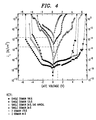
- FIG. 4 is a plot of leakage current density, J L , as a function of gate voltage, for various Gd 2 O 3 dielectric layers under various conditions. Both two-domain and single domain films are represented, and also included in FIG. 4 is plot of leakage current/gate voltage for a single-domain 34 ⁇ thick Gd 2 O 3 film subsequent to a post-forming gas anneal at a temperature of 400°C for one hour (labeled as "D" in FIG. 4). Referring to FIG. 4, it is apparent that the leakage current density is essentially symmetric about an unbiased gate (i.e., a 0V applied voltage). The leakage current density of two-domain dielectric films is shown to be significantly higher than that associated with single domain films, particularly for dielectrics thinner than 100 ⁇ .
- the leakage current density for a two-domain film 44 ⁇ thick can be as high as 10 -3 A/cm 2 at zero bias.
- the leakage current density of the single domain dielectrics is markedly improved, particularly at smaller film thicknesses.
- J L at 1V for a 34 ⁇ thick film is reduced from a value of approximately ⁇ 10 -1 A/cm 2 for a two-domain film to a value of about 10 -3 A/com 2 for a single domain dielectric.
- subjecting the grown dielectric to a post-forming gas anneal (a combination of N 2 and H2) will further improve (that is, decrease) the leakage current density.
- the forming gas anneal on the single domain 34 ⁇ film results in further improving the leakage current density to a value of about 10 -5 A/cm 2 .
- amorphous dielectric films may be more appropriate for device applications than crystalline films, due to the absence of domain boundaries and the lack of surface or interfacial stress in the latter. Additionally, while the leakage currents of amorphous Gd 2 O 3 films are comparable to the amorphous Y 2 O 3 films, Y 2 O 3 shows a more consistent dielectric behavior than Gd 2 O 3 , in that the dielectric constant of Y 2 O 3 remains essentially constant at about 18, insensitive to thickness reductions.
- FIG. 5 shows the dependence of J L on V for a series of amorphous Y 2 O 3 films.
- an as-deposited amorphous Y 2 O 3 film 45 ⁇ thick yields a relatively low leakage current density of 10 -6 A/cm 2 at 1V for an equivalent SiO 2 thickness ("t eq ") of only 10 ⁇ .
- the leakage current density improves by another order of magnitude after a forming gas anneal (at a temperature of, for example, 400°C for about one hour).
- the resulting value is about five orders of magnitude better than the best data associated with conventional 15 ⁇ thick SiO 2 dielectrics.
- performing a rapid thermal anneal (RTA) at 1000°C for about one minute shows that the Y 2 O 3 film remains essentially stable.
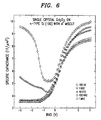
- the specific capacitance (C/A) versus voltage data for an MOS diode including a Gd 2 O 3 single domain, 196 ⁇ thick gate dielectric (after a forming gas anneal) is shown in FIG. 6 as a function of frequency ranging from 100Hz to 1 MHz.
- the dielectric constant (s) for such a film was measured to exhibit a value of approximately 20.
- a transition in MOS diode behavior from accumulation to depletion mode occurs at approximately 2V. the inversions of the carriers (holes) is evident, and follows the AC signal up to a frequency of 10kHz.
- FIG. 6 The specific capacitance (C/A) versus voltage data for an MOS diode including a Gd 2 O 3 single domain, 196 ⁇ thick gate dielectric (after a forming gas anneal) is shown in FIG. 6 as a function of frequency ranging from 100Hz to 1 MHz.
- the dielectric constant (s) for such a film was measured to exhibit a value of approximately 20.
- the capacitor 7 illustrates the C/A versus V data for a 45 ⁇ thick amorphous Y 2 O 3 film (after g a post-growth forming gas anneal).
- the capacitor has a C/A value as high as 35-40 fF/ ⁇ m 2 , comparable to a 10 ⁇ thick SiO 2 equivalent (or better). It is to be noted that the dielectric constant associated with this material remains at a value of 18 even at this thin layer.
Abstract
Description
- The present invention relates to an improved gate oxide material, and method of forming the same, for silicon-based devices and, more particularly, to the use of rare earth oxides, such as Gd2O3 or Y2O3 (exhibiting a dielectric constant ε on the order of 18) to form a gate oxide having the desired insulative properties while maintaining a thickness greater than the tunneling depth of approximately 10Å.
- As integrated circuit technology advances, the gate lengths of MOSFETs become increasingly smaller. In addition, the thicknesses of the gate dielectrics, typically gate oxides, become thinner and thinner. Very thin gate oxides (i.e., less than 50Å) are often necessary for sub-micron MOS devices.
- As device dimensions scale down rapidly with the advance of technology, the electric field in the thin gate oxides continues to increase. Part of the consequences of such increased electric field is the increased trap generation at the oxide interface or within the thin oxides. The trap generation and the capture of channel electrons by the traps in turn leads to increased low frequency (1/f) noise and transconductance (gm) degradation. For ultra-thin gate oxides of less than 50Å, the tunneling current also becomes significant and gives rise to accelerated degradation of the device characteristics. Indeed, the "thinness" of the conventional SiO2 gate oxide is now approaching the quantum tunneling limit of 10Å.
- Instead of continuously attempting to reduce the SiO2 thickness of the gate oxide, several groups have attempted to find a replacement insulator with a dielectric constant (ε) substantially greater than that of SiO2 (ε = 3.9), so that the dielectric thickness can then be proportionally increased (thereby reducing the chance of a tunneling current through the oxide). It is desirable that the dielectric being thermodynamically stable with respect to the silicon surface so as to prevent reactions leading to the formation of SiO2 or metal silicides at the substrate/dielectric interface during high temperature annealing operations. To date, several "high dielectric" oxides have been considered (such as Al2O3, Ta2O3, TiO2), but in each case an interfacial SiO2 layer at least 10Å thick forms during growth of the gate oxide. An alternative approach uses a relatively thin SiNx barrier layer that is first deposited on the silicon surface to prevent the native oxide growth. However, the use of the barrier layer then requires for the total "effective" oxide thickness to exceed 15Å, another unacceptable result.
- Thus, a need remains in the art for a dielectric material to be used as a "thin" gate dielectric on silicon-based devices that prevents the formation of the native SiO2 layer., yet also exhibits an effective thickness closer to 10Å.
- The need remaining in the prior art is addressed by the present invention, which relates to an improved gate oxide material, and method of forming the same, for silicon-based devices and, more particularly, to the use of rare earth oxides, such as Gd2O3 or Y2O3 (exhibiting a dielectric constant s significantly greater than that of SiO2 (approximately 4), for example, on the order of 18) to form a gate oxide having the desired insulative properties while maintaining a thickness greater than the tunneling depth of approximately 10Å.
- Films of Gd2O3 or Y2O3 are grown, in accordance with the present invention, on a "clean" silicon substrate surface, using an ultrahigh vacuum (UHV) vapor deposition process. It has been found that by limiting the oxygen partial pressure to less than 10-7 during growth, oxidation of the silicon substrate surface is completely avoided. Both epitaxial and amorphous films have been found to form an oxide with the desired high dielectric constant characteristic.
- In accordance with the present invention, a vicinal Si(100) substrate is preferably used, so as to promote the formation of single domain, (110)-oriented Gd2O3 or Y2O3 films. In a preferred embodiment a 4° miscut substrate may be used.
- A post-process gas anneal process may also be used to improve the leakage current density from a value of, for example, 10-1 A/cm2 to 10-5 A/cm2 at 1V for a Gd2O3 layer at an equivalent SiO2 thickness of 19Å.
- Other and further aspects of the present invention will become apparent during the following discussion and by reference to the accompanying drawings.
- Referring now to the drawings,
- FIG. 1 illustrates an exemplary vicinal silicon substrate that is preferable for supporting growth of a high dielectric gate oxide of the present invention;
- FIG. 2 contains a graph of an X-ray diffraction scan across a set of three different (110) Gd2O3 single domain films;
- FIG. 3 shows the {222} reflections resulting from both degenerate orientations of Gd2O3 films, illustrating the relationship between film thickness and domination of a preferred orientation;
- FIG. 4 contains a graph of leakage current density (JL) versus voltage (V) for crystalline Gd2O3 films;
- FIG. 5 is a graph of leakage current density versus voltage for amorphous Y2O3 films;
- FIG. 6 illustrates specific capacitance as a function of voltage for single crystal Gd2O3 grown on a vicinal silicon substrate; and
- FIG. 7 illustrates specific capacitance as a function of voltage for amorphous Y2O3 grown on a conventional silicon substrate.
-
- Rare earth oxides are suitable candidates for various semiconductor applications, based on thermodynamic energy considerations. In accordance with the present invention, it has been found possible to form the dielectrics Gd2O3 (ε~12) or Y2O3 (e ~18) as gate oxides on a silicon (100) surface. Both materials exhibit the required "high" dielectric when compared to that of SiO2 (ε=3.9), although Y2O3 is considered to be preferred due to its higher dielectric constant and the absence of magnetic ions in the oxide.
- An important aspect of the present invention is the use of vicinal Si(100) substrates to eliminate the formation of unwanted domains in the grown oxides, thus providing a single domain, (110)-oriented gate oxide. FIG. 1 illustrates an exemplary vicinal Si(100)
substrate 10, which has been "miscut" at a predetermined tilt angle, where a tilt angle in the range of 4-6° has been found to be preferable. Themiscut surface 12 exposessurface steps 14 of double atomic layers, thus giving mono-domain silicon terraces of a spacing approximately 80Å (for a 4° miscut) for nucleating the growth of a single variant of either Gd2O3 or Y2O3. - In forming the high dielectric gate oxide structure of the present invention, a multi-chamber ultra-high vacuum system may be used. Prior to growing the dielectric, the silicon wafer is cleaned and then hydrogen passivated (using a buffered HF acid, for example) to form a surface free of impurities. The substrate is then heated to a temperature in the range of, for example, 450 - 500 °C, allowing the generation of a silicon surface free of impurities or oxides. Powder-packed ceramic sources of Gd2O3. or Y2O3 are then used as electron beam sources in the UHV system to provide deposition of the desired epitaxial dielectric film. In accordance with one aspect of the present invention, the oxygen partial pressure within the UHV chamber needs to be maintained at less than 10-7 torr during growth, where such a pressure has been found to essentially eliminate the formation of a native SiO2 layer at the interface between the substrate and dielectric. As mentioned above, the capability of controlling the structure and chemistry of the interface at the atomic layer scale is critical.
- The presence/lack of such a native oxide film has been studied by carrying out an infrared absorption analysis of Gd2O3 oxide films and the associated interface with the underlying silicon substrate. To maintain the integrity of the Gd2O3 film during the analysis, a thin amorphous silicon film was deposited in-situ on the Gd2O3 film prior to atmosphere exposure. The presence of this silicon film made it possible to HF-etch both the amorphous front and crystalline back silicon surfaces, leaving them H-terminated and insuring only an interface native oxide would contribute to an IR absorption spectrum. For comparison, each wafer containing a Gd2O3 dielectric film was reference to a similarly HF-etched silicon substrate - without a Gd2O3 film deposition. The absorption results clearly show a Gd2O3 phonon band at 600 cm-1, where its intensity scales with film thickness. There was a lack of any measurable SiO2-related features at either the TO (1050 cm-1) or LO (1200-1250 cm-1) frequencies of SiO2, for crystalline as well as amorphous Gd2O3 samples.
- Crystals of Gd2O3 and Y2O3 have an isomorphic Mn2O3 structure with a large lattice constant (10.81 Å and 10.60 Å, respectively). Studies have shown that an (110)-oriented Gd2O3 and Y2O3 of two-fold symmetry will grow on a conventional (100) silicon surface of four-fold symmetry, leading to the unwanted formation of two (110) variants of equal probability in the growth plane. In particular, the growth of these two variants with equal probability results in an oxide with a relatively high leakage current, and is clearly not favorable for device consideration. In accordance with the present invention, the two-fold degeneracy is removed by using the vicinal silicon substrate, as illustrated in FIG. 1.
- Post-growth processing may also be employed in the method of the present invention, where as will be discussed in more detail below, a post-forming gas anneal has been shown to provide an improvement in leakage current density from 10-1 A/cm2 to 10-5 A/cm2 at 1V for a
Gd 203 layer at an equivalent SiO2 thickness of 19Å. An amorphous Y2O3 film can be formed on a conventional silicon surface that exhibits a leakage current as low as 10-6 A/cm2 at 1V for an SiO2 equivalent thickness of 10Å. - FIG. 2 illustrates a longitudinal x-ray diffraction scan along the surface of three different Gd2O3 films. Scan A of FIG. 2 is associated with a Gd2O3 film of thickness 34Å, scan B with a Gd2O3 film of thickness 125Å, and scan C with a Gd2O3 film having a thickness of 196Å. Referring to FIG. 2, the fringe patterns on each scan can be attributed to coherent interference between the air/oxide and oxide/silicon interfaces. While the fringe period is inversely proportional to the film thickness, the decay of the fringe amplitude is a measure of the film thickness uniformity. Thus, the slow decay as shown in each scan leads to the conclusion that each of the grown Gd2O3 films is extremely uniform. The various oxide thicknesses discussed with respect to FIG. 2 (as well as the following figures) are considered to be exemplary only. In general, high dielectric oxides formed in accordance with the present invention may comprise a thickness anywhere within the range of, for example 10 - 500 Å and provide the desired gate dielectric properties for all intended device applications.
- Gd2O3 gate dielectric films grown on vicinal (100) silicon substrates in accordance with the present invention have been found to exhibit a broad peak near 2 = 47.5° for the (440) reflection, with the peak becoming sharper with increasing film thickness. FIG. 3 illustrates in particular a set of 360° scan about the surface normal for the in-plane components of the {222} reflection for the set of three different Gd2O3 films associated with FIG. 2. In each case, the grown dielectric is predominantly oriented in one type of domain, with the [001] axis of the Gd2O3 parallel to the silicon step edges 16 (see FIG. 1), that is, the [110] axis of
miscut substrate 10. The {222} reflections illustrated in FIG. 3 for each dielectric thickness illustrate peaks associated with both orientations. The two weak peaks, denoted w1 and w2 in FIG. 3, are separated by π with respect to the two strong peaks, denoted s1 and s2. An analysis of the data in FIG. 3 yields the conclusion that nearly 95% of the 34Å thick Gd2O3 dielectric is grown in the preferred ("strong") orientation, with the percentage increasing to approximately 99% for the thicker 196Å film. The analysis leads to the conclusion that beyond some "critical" thickness (approximately 100Å), domains with the undesired orientation begin to get buried beneath the still-growing oxide. - FIG. 4 is a plot of leakage current density, JL, as a function of gate voltage, for various Gd2O3 dielectric layers under various conditions. Both two-domain and single domain films are represented, and also included in FIG. 4 is plot of leakage current/gate voltage for a single-domain 34Å thick Gd2O3 film subsequent to a post-forming gas anneal at a temperature of 400°C for one hour (labeled as "D" in FIG. 4). Referring to FIG. 4, it is apparent that the leakage current density is essentially symmetric about an unbiased gate (i.e., a 0V applied voltage). The leakage current density of two-domain dielectric films is shown to be significantly higher than that associated with single domain films, particularly for dielectrics thinner than 100Å. As shown, the leakage current density for a two-domain film 44Å thick can be as high as 10-3 A/cm2 at zero bias. The leakage current density of the single domain dielectrics is markedly improved, particularly at smaller film thicknesses. For example, JL at 1V for a 34Å thick film is reduced from a value of approximately ≥ 10-1 A/cm2 for a two-domain film to a value of about 10-3 A/com2 for a single domain dielectric. As mentioned above, subjecting the grown dielectric to a post-forming gas anneal (a combination of N2 and H2) will further improve (that is, decrease) the leakage current density. As shown in FIG. 4, the forming gas anneal on the single domain 34Å film results in further improving the leakage current density to a value of about 10-5 A/cm2.
- A study of amorphous dielectric films suggests that these films may be more appropriate for device applications than crystalline films, due to the absence of domain boundaries and the lack of surface or interfacial stress in the latter. Additionally, while the leakage currents of amorphous Gd2O3 films are comparable to the amorphous Y2O3 films, Y2O3 shows a more consistent dielectric behavior than Gd2O3, in that the dielectric constant of Y2O3 remains essentially constant at about 18, insensitive to thickness reductions. FIG. 5 shows the dependence of JL on V for a series of amorphous Y2O3 films. As shown, an as-deposited amorphous Y2O3 film 45Å thick yields a relatively low leakage current density of 10-6 A/cm2 at 1V for an equivalent SiO2 thickness ("teq") of only 10Å. The leakage current density improves by another order of magnitude after a forming gas anneal (at a temperature of, for example, 400°C for about one hour). The resulting value is about five orders of magnitude better than the best data associated with conventional 15Å thick SiO2 dielectrics. Beyond this leakage current density, performing a rapid thermal anneal (RTA) at 1000°C for about one minute shows that the Y2O3 film remains essentially stable.
- The specific capacitance (C/A) versus voltage data for an MOS diode including a Gd2O3 single domain, 196Å thick gate dielectric (after a forming gas anneal) is shown in FIG. 6 as a function of frequency ranging from 100Hz to 1 MHz. The dielectric constant (s) for such a film was measured to exhibit a value of approximately 20. As shown, a transition in MOS diode behavior from accumulation to depletion mode occurs at approximately 2V. the inversions of the carriers (holes) is evident, and follows the AC signal up to a frequency of 10kHz. FIG. 7 illustrates the C/A versus V data for a 45Å thick amorphous Y2O3 film (after g a post-growth forming gas anneal). The capacitor has a C/A value as high as 35-40 fF/µm2, comparable to a 10Å thick SiO2 equivalent (or better). It is to be noted that the dielectric constant associated with this material remains at a value of 18 even at this thin layer.
- The invention has been described with reference to particular preferred embodiments, but variations will occur to those skilled in the art. For example, while Gd2O3 and Y2O3 have been discussed in detail, various other rare earth oxides of the form Mn2O3, in both single crystal and amorphous form, may also be used to create high dielectric gate oxides in accordance with the principles of the present invention.
Claims (29)
- A semiconductor device comprisinga vicinal silicon (100) substrate exhibiting a predetermined angular miscut so as to form a top major surface exhibiting a staircase pattern along the [110] direction; anda rare earth oxide of the form Mn2O3, exhibiting a dielectric constant ε≥4, deposited, under an oxygen partial pressure less than 10-7 torr, to a predetermined thickness t on the staircase major surface of said vicinal silicon substrate without forming an SiO2 film therebetween.
- A semiconductor device as defined in claim 1 wherein the rare earth oxide comprises Gd2O3.
- A semiconductor device as defined in claim 2 wherein the Gd2O3 comprises epitaxial Gd2O3.
- A semiconductor device as defined in claim 2 wherein the rare earth oxide comprises a two-domain (100) Gd2O3 structure.
- A semiconductor device as defined in claim 2 wherein the rare earth oxide comprises a single domain (100) Gd2O3 structure.
- A semiconductor device as defined in claim 1 wherein the rare earth oxide comprises Y203.
- A semiconductor device as defined in claim 6 wherein the Y2O3 comprises epitaxial Y2O3.
- A semiconductor device as defined in claim 6 wherein the rare earth oxide comprises a two-domain (100) Y2O3 structure.
- A semiconductor device as defined in claim 6 wherein the rare earth oxide comprises a single domain (100) Y2O3 structure.
- A semiconductor device as defined in claim 1 wherein the rare earth oxide is formed to comprise a thickness in the range of 10Å to 500Å.
- A semiconductor device as defined in claim 1 wherein the vicinal silicon substrate comprises a predetermined angular miscut in the range of 4-6°.
- A semiconductor device as defined in claim 11 wherein the predetermined angular miscut is approximately 4°, forming a terrace spacing on the silicon substrate major surface of approximately 80Å.
- A semiconductor device comprisinga silicon substrate defined as comprising a top major surface; andan amorphous rare earth oxide of the form Mn2O3 and exhibiting a dielectric constant ε≥4 deposited, under an oxygen partial pressure less than 10-7 torr, to a predetermined thickness t on the top major surface of the silicon substrate without forming an SiO2 film therebetween.
- A semiconductor device as defined in claim 13 wherein the amorphous rare earth oxide comprises Gd2O3.
- A semiconductor device as defined in claim 13 wherein the amorphous rare earth oxide comprises Y2O3.
- A method of forming a semiconductor device include a high dielectric oxide layer, the method comprising the steps of:a) providing a vicinal silicon (100) substrate illustrating a predetermined angular miscut on a major surface thereof so as to form a staircase pattern on said major surface;b) cleaning said silicon major surface to remove impurities and oxides;c) inserting said substrate in an ultra-high vacuum system including an oxygen ambient atmosphere;d) providing a ceramic rare earth oxide source;e) reducing the oxygen partial pressure in said ultra-high vacuum system to a level less than or equal to 10-7 torr;f) electron-beam evaporating a predetermined thickness of said ceramic rare earth oxide onto said staircase-patterned major surface of said vicinal silicon substrate.
- The method as defined in claim 16 wherein in performing step a), the vicinal silicon (100) substrate is miscut to a predetermined angle in the range of 4-6°.
- The method as defined in claim 17 wherein in performing step a) the vicinal silicon (100) substrate is miscut to a predetermined angle of approximately 4°, forming a staircase pattern having a step height of approximately 80Å.
- The method as defined in claim 16 wherein in performing step b), the silicon substrate is cleaned by hydrogen passivation with a buffered-HF solution.
- The method as defined in claim 16 wherein in performing step d), ceramic Gd2O3 is provided.
- The method as defined in claim 16 wherein in performing step d), ceramic Y2O3 is provided.
- The method as defined in claim 16 wherein in performing step f), a rare earth oxide layer having a thickness in the range of 10Å - 500Å is formed.
- The method as defined in claim 16 wherein the method further comprises the step of:
g) gas annealing the rare earth oxide dielectric layer at a predetermined temperature and for a predetermined time sufficient to decrease the leakage current density to a predefined value. - The method as defined in claim 23 wherein in performing step g), the device is heated to a temperature of approximately 400°C for approximately one hour.
- The method as defined in claim 23 wherein in performing step g), the gas anneal is a predefined mixture of H2 and N2.
- The method as defined in claim 23 wherein in performing step g), a rapid thermal anneal at a temperature of approximately 1000°C for approximately one minute is performed.
- A method of forming a semiconductor device include a high dielectric oxide layer, the method comprising the steps of:a) providing a silicon (100) defined as including a top major surface;b) cleaning said silicon top major surface to remove impurities and oxides;c) inserting said substrate in an ultra-high vacuum system including an oxygen ambient atmosphere;d) providing a ceramic rare earth oxide source;e) reducing the oxygen partial pressure in said ultra-high vacuum system to a level less than or equal to 10-7 torr;f) electron-beam evaporating a predetermined thickness of said ceramic rare earth oxide to form an amorphous rare earth oxide layer on said silicon top major surface.
- The method as defined in claim 27 wherein in performing step d), ceramic Gd2O3 is provided.
- The method as defined in claim 27 wherein in performing step d), ceramic Y2O3 is provided.
Applications Claiming Priority (2)
| Application Number | Priority Date | Filing Date | Title |
|---|---|---|---|
| US499411 | 2000-02-07 | ||
| US09/499,411 US6404027B1 (en) | 2000-02-07 | 2000-02-07 | High dielectric constant gate oxides for silicon-based devices |
Publications (2)
| Publication Number | Publication Date |
|---|---|
| EP1122795A2 true EP1122795A2 (en) | 2001-08-08 |
| EP1122795A3 EP1122795A3 (en) | 2002-10-09 |
Family
ID=23985160
Family Applications (1)
| Application Number | Title | Priority Date | Filing Date |
|---|---|---|---|
| EP01300746A Withdrawn EP1122795A3 (en) | 2000-02-07 | 2001-01-29 | High dielectric constant gate oxides for silicon-based devices |
Country Status (5)
| Country | Link |
|---|---|
| US (1) | US6404027B1 (en) |
| EP (1) | EP1122795A3 (en) |
| JP (1) | JP2001284349A (en) |
| KR (1) | KR20010078345A (en) |
| TW (1) | TW550734B (en) |
Cited By (7)
| Publication number | Priority date | Publication date | Assignee | Title |
|---|---|---|---|---|
| US7208804B2 (en) * | 2001-08-30 | 2007-04-24 | Micron Technology, Inc. | Crystalline or amorphous medium-K gate oxides, Y203 and Gd203 |
| WO2008109236A1 (en) * | 2007-03-05 | 2008-09-12 | Translucent Photonics, Inc. | Heterogeneous semiconductor substrate |
| US7759237B2 (en) | 2007-06-28 | 2010-07-20 | Micron Technology, Inc. | Method of forming lutetium and lanthanum dielectric structures |
| US7804144B2 (en) | 2001-12-20 | 2010-09-28 | Micron Technology, Inc. | Low-temperature grown high quality ultra-thin CoTiO3 gate dielectrics |
| US7867919B2 (en) | 2004-08-31 | 2011-01-11 | Micron Technology, Inc. | Method of fabricating an apparatus having a lanthanum-metal oxide dielectric layer |
| US8026161B2 (en) | 2001-08-30 | 2011-09-27 | Micron Technology, Inc. | Highly reliable amorphous high-K gate oxide ZrO2 |
| US8501563B2 (en) | 2005-07-20 | 2013-08-06 | Micron Technology, Inc. | Devices with nanocrystals and methods of formation |
Families Citing this family (34)
| Publication number | Priority date | Publication date | Assignee | Title |
|---|---|---|---|---|
| US7554829B2 (en) | 1999-07-30 | 2009-06-30 | Micron Technology, Inc. | Transmission lines for CMOS integrated circuits |
| US6693033B2 (en) | 2000-02-10 | 2004-02-17 | Motorola, Inc. | Method of removing an amorphous oxide from a monocrystalline surface |
| US7273657B2 (en) * | 2000-08-08 | 2007-09-25 | Translucent Photonics, Inc. | Rare earth-oxides, rare earth-nitrides, rare earth-phosphides and ternary alloys with silicon |
| US6638838B1 (en) | 2000-10-02 | 2003-10-28 | Motorola, Inc. | Semiconductor structure including a partially annealed layer and method of forming the same |
| US20020096683A1 (en) * | 2001-01-19 | 2002-07-25 | Motorola, Inc. | Structure and method for fabricating GaN devices utilizing the formation of a compliant substrate |
| US6673646B2 (en) | 2001-02-28 | 2004-01-06 | Motorola, Inc. | Growth of compound semiconductor structures on patterned oxide films and process for fabricating same |
| US6709989B2 (en) | 2001-06-21 | 2004-03-23 | Motorola, Inc. | Method for fabricating a semiconductor structure including a metal oxide interface with silicon |
| US6852575B2 (en) * | 2001-07-05 | 2005-02-08 | International Business Machines Corporation | Method of forming lattice-matched structure on silicon and structure formed thereby |
| US6933566B2 (en) * | 2001-07-05 | 2005-08-23 | International Business Machines Corporation | Method of forming lattice-matched structure on silicon and structure formed thereby |
| US6646293B2 (en) | 2001-07-18 | 2003-11-11 | Motorola, Inc. | Structure for fabricating high electron mobility transistors utilizing the formation of complaint substrates |
| US6693298B2 (en) | 2001-07-20 | 2004-02-17 | Motorola, Inc. | Structure and method for fabricating epitaxial semiconductor on insulator (SOI) structures and devices utilizing the formation of a compliant substrate for materials used to form same |
| US6667196B2 (en) | 2001-07-25 | 2003-12-23 | Motorola, Inc. | Method for real-time monitoring and controlling perovskite oxide film growth and semiconductor structure formed using the method |
| US6639249B2 (en) | 2001-08-06 | 2003-10-28 | Motorola, Inc. | Structure and method for fabrication for a solid-state lighting device |
| US6673667B2 (en) | 2001-08-15 | 2004-01-06 | Motorola, Inc. | Method for manufacturing a substantially integral monolithic apparatus including a plurality of semiconductor materials |
| US6900122B2 (en) * | 2001-12-20 | 2005-05-31 | Micron Technology, Inc. | Low-temperature grown high-quality ultra-thin praseodymium gate dielectrics |
| JP2003282439A (en) | 2002-03-27 | 2003-10-03 | Seiko Epson Corp | Substrate for device and manufacturing method thereof |
| US7045430B2 (en) | 2002-05-02 | 2006-05-16 | Micron Technology Inc. | Atomic layer-deposited LaAlO3 films for gate dielectrics |
| US7160577B2 (en) | 2002-05-02 | 2007-01-09 | Micron Technology, Inc. | Methods for atomic-layer deposition of aluminum oxides in integrated circuits |
| US6916717B2 (en) * | 2002-05-03 | 2005-07-12 | Motorola, Inc. | Method for growing a monocrystalline oxide layer and for fabricating a semiconductor device on a monocrystalline substrate |
| US7205218B2 (en) | 2002-06-05 | 2007-04-17 | Micron Technology, Inc. | Method including forming gate dielectrics having multiple lanthanide oxide layers |
| US6790791B2 (en) | 2002-08-15 | 2004-09-14 | Micron Technology, Inc. | Lanthanide doped TiOx dielectric films |
| US7192892B2 (en) | 2003-03-04 | 2007-03-20 | Micron Technology, Inc. | Atomic layer deposited dielectric layers |
| US7135369B2 (en) * | 2003-03-31 | 2006-11-14 | Micron Technology, Inc. | Atomic layer deposited ZrAlxOy dielectric layers including Zr4AlO9 |
| US7192824B2 (en) | 2003-06-24 | 2007-03-20 | Micron Technology, Inc. | Lanthanide oxide / hafnium oxide dielectric layers |
| WO2005065357A2 (en) * | 2003-12-29 | 2005-07-21 | Translucent, Inc. | Rare earth-oxides, rare-earth-nitrides, rare earth-phosphides and ternary alloys with silicon |
| US7081421B2 (en) | 2004-08-26 | 2006-07-25 | Micron Technology, Inc. | Lanthanide oxide dielectric layer |
| US7588988B2 (en) | 2004-08-31 | 2009-09-15 | Micron Technology, Inc. | Method of forming apparatus having oxide films formed using atomic layer deposition |
| US7235501B2 (en) | 2004-12-13 | 2007-06-26 | Micron Technology, Inc. | Lanthanum hafnium oxide dielectrics |
| US7399666B2 (en) * | 2005-02-15 | 2008-07-15 | Micron Technology, Inc. | Atomic layer deposition of Zr3N4/ZrO2 films as gate dielectrics |
| US7687409B2 (en) | 2005-03-29 | 2010-03-30 | Micron Technology, Inc. | Atomic layer deposited titanium silicon oxide films |
| US7390756B2 (en) | 2005-04-28 | 2008-06-24 | Micron Technology, Inc. | Atomic layer deposited zirconium silicon oxide films |
| US7662729B2 (en) | 2005-04-28 | 2010-02-16 | Micron Technology, Inc. | Atomic layer deposition of a ruthenium layer to a lanthanide oxide dielectric layer |
| US7675117B2 (en) * | 2006-11-14 | 2010-03-09 | Translucent, Inc. | Multi-gate field effect transistor |
| JP5100313B2 (en) * | 2007-10-31 | 2012-12-19 | 株式会社東芝 | Method for producing lanthanum oxide compound |
Family Cites Families (8)
| Publication number | Priority date | Publication date | Assignee | Title |
|---|---|---|---|---|
| US3663870A (en) * | 1968-11-13 | 1972-05-16 | Tokyo Shibaura Electric Co | Semiconductor device passivated with rare earth oxide layer |
| JPS6210757A (en) * | 1985-07-09 | 1987-01-19 | Panafacom Ltd | Processor control system |
| US4707216A (en) * | 1986-01-24 | 1987-11-17 | University Of Illinois | Semiconductor deposition method and device |
| US4872046A (en) | 1986-01-24 | 1989-10-03 | University Of Illinois | Heterojunction semiconductor device with <001> tilt |
| JPS63140577A (en) * | 1986-12-02 | 1988-06-13 | Toshiba Corp | Field effect transistor |
| JPH07169127A (en) * | 1993-10-01 | 1995-07-04 | Minnesota Mining & Mfg Co <3M> | Amorphous rare-earth oxide |
| TW328147B (en) | 1996-05-07 | 1998-03-11 | Lucent Technologies Inc | Semiconductor device fabrication |
| JP3813740B2 (en) * | 1997-07-11 | 2006-08-23 | Tdk株式会社 | Substrates for electronic devices |
-
2000
- 2000-02-07 US US09/499,411 patent/US6404027B1/en not_active Expired - Lifetime
-
2001
- 2001-01-29 EP EP01300746A patent/EP1122795A3/en not_active Withdrawn
- 2001-02-01 TW TW090102046A patent/TW550734B/en active
- 2001-02-06 KR KR1020010005610A patent/KR20010078345A/en not_active Application Discontinuation
- 2001-02-07 JP JP2001030331A patent/JP2001284349A/en active Pending
Non-Patent Citations (6)
| Title |
|---|
| CHOI S C ET AL: "EPITAXIAL GROWTH OF Y2O3 FILMS ON SI(100) WITHOUT AN INTERFACIAL OXIDE LAYER" APPLIED PHYSICS LETTERS, AMERICAN INSTITUTE OF PHYSICS. NEW YORK, US, vol. 71, no. 7, 18 August 1997 (1997-08-18), pages 903-905, XP000720061 ISSN: 0003-6951 * |
| HIROFUMI FUKUMOTO ET AL: "HETEROEPITAXIAL GROWTH OF Y2O3 FILMS ON SILICON" APPLIED PHYSICS LETTERS, AMERICAN INSTITUTE OF PHYSICS. NEW YORK, US, vol. 55, no. 4, 24 July 1989 (1989-07-24), pages 360-361, XP000126662 ISSN: 0003-6951 * |
| KALKUR T S ET AL: "YTTRIUM OXIDE BASED METAL-INSULATOR-SEMICONDUCTOR STRUCTURES ON SILICON" THIN SOLID FILMS, ELSEVIER-SEQUOIA S.A. LAUSANNE, CH, vol. 170, no. 2, INDEX, 15 March 1989 (1989-03-15), pages 185-189, XP000035671 ISSN: 0040-6090 * |
| KIM H B ET AL: "Oxygen distribution in the heteroepitaxially grown Y2O3 films on Si substrates" NUCLEAR INSTRUMENTS & METHODS IN PHYSICS RESEARCH, SECTION - B: BEAM INTERACTIONS WITH MATERIALS AND ATOMS, NORTH-HOLLAND PUBLISHING COMPANY. AMSTERDAM, NL, vol. 142, no. 3, July 1998 (1998-07), pages 393-396, XP004148825 ISSN: 0168-583X * |
| KWO J ET AL: "HIGH EPSILON GATE DIELECTRICS GD2O3 AND Y2O3 FOR SILICON" APPLIED PHYSICS LETTERS, AMERICAN INSTITUTE OF PHYSICS. NEW YORK, US, vol. 77, no. 1, 3 July 2000 (2000-07-03), pages 130-132, XP000958525 ISSN: 0003-6951 * |
| SHARMA R N ET AL: "ELECTRICAL BEHAVIOUR OF ELECTRON-BEAM-EVAPORATED YTTRIUM OXIDE THIN FILMS ON SILICON" THIN SOLID FILMS, ELSEVIER-SEQUOIA S.A. LAUSANNE, CH, vol. 199, no. 1, 1 April 1991 (1991-04-01), pages 1-8, XP000201737 ISSN: 0040-6090 * |
Cited By (12)
| Publication number | Priority date | Publication date | Assignee | Title |
|---|---|---|---|---|
| US7208804B2 (en) * | 2001-08-30 | 2007-04-24 | Micron Technology, Inc. | Crystalline or amorphous medium-K gate oxides, Y203 and Gd203 |
| US8026161B2 (en) | 2001-08-30 | 2011-09-27 | Micron Technology, Inc. | Highly reliable amorphous high-K gate oxide ZrO2 |
| US8652957B2 (en) | 2001-08-30 | 2014-02-18 | Micron Technology, Inc. | High-K gate dielectric oxide |
| US7804144B2 (en) | 2001-12-20 | 2010-09-28 | Micron Technology, Inc. | Low-temperature grown high quality ultra-thin CoTiO3 gate dielectrics |
| US8178413B2 (en) | 2001-12-20 | 2012-05-15 | Micron Technology, Inc. | Low-temperature grown high quality ultra-thin CoTiO3 gate dielectrics |
| US7867919B2 (en) | 2004-08-31 | 2011-01-11 | Micron Technology, Inc. | Method of fabricating an apparatus having a lanthanum-metal oxide dielectric layer |
| US8501563B2 (en) | 2005-07-20 | 2013-08-06 | Micron Technology, Inc. | Devices with nanocrystals and methods of formation |
| US8921914B2 (en) | 2005-07-20 | 2014-12-30 | Micron Technology, Inc. | Devices with nanocrystals and methods of formation |
| WO2008109236A1 (en) * | 2007-03-05 | 2008-09-12 | Translucent Photonics, Inc. | Heterogeneous semiconductor substrate |
| US7759237B2 (en) | 2007-06-28 | 2010-07-20 | Micron Technology, Inc. | Method of forming lutetium and lanthanum dielectric structures |
| US8071443B2 (en) | 2007-06-28 | 2011-12-06 | Micron Technology, Inc. | Method of forming lutetium and lanthanum dielectric structures |
| US8847334B2 (en) | 2007-06-28 | 2014-09-30 | Micron Technology, Inc. | Method of forming lutetium and lanthanum dielectric structures |
Also Published As
| Publication number | Publication date |
|---|---|
| EP1122795A3 (en) | 2002-10-09 |
| KR20010078345A (en) | 2001-08-20 |
| JP2001284349A (en) | 2001-10-12 |
| TW550734B (en) | 2003-09-01 |
| US6404027B1 (en) | 2002-06-11 |
Similar Documents
| Publication | Publication Date | Title |
|---|---|---|
| US6404027B1 (en) | High dielectric constant gate oxides for silicon-based devices | |
| Kwo et al. | Properties of high κ gate dielectrics Gd 2 O 3 and Y 2 O 3 for Si | |
| US6586797B2 (en) | Graded composition gate insulators to reduce tunneling barriers in flash memory devices | |
| US4859253A (en) | Method for passivating a compound semiconductor surface and device having improved semiconductor-insulator interface | |
| Harris et al. | HfO 2 gate dielectric with 0.5 nm equivalent oxide thickness | |
| JP3299657B2 (en) | Gallium oxide thin film | |
| Fissel et al. | Towards understanding epitaxial growth of alternative high-K dielectrics on Si (001): Application to praseodymium oxide | |
| EP1001468A1 (en) | Rare earth oxide layer on a GaAs- or GaN-based semiconductor body | |
| Ramanathan et al. | Growth and characterization of ultrathin zirconia dielectrics grown by ultraviolet ozone oxidation | |
| EP0840362A1 (en) | Fabrication of tungsten gate electrodes by means of tungsten carbonyl | |
| US6613677B1 (en) | Long range ordered semiconductor interface phase and oxides | |
| US6605151B1 (en) | Oxide thin films and composites and related methods of deposition | |
| Batey et al. | Plasma-enhanced CVD of high quality insulating films | |
| Herbots et al. | The formation of ordered, ultrathin SiO2/Si (1 0 0) interfaces grown on (1× 1) Si (1 0 0) | |
| Fukumoto et al. | Electrical characteristics of metal‐insulator‐semiconductor diodes with ZrO2/SiO2 dielectric films | |
| Sharma et al. | Compositional and electronic properties of chemical‐vapor‐deposited Y2O3 thin film‐Si (100) interfaces | |
| US7678633B2 (en) | Method for forming substrates for MOS transistor components and its products | |
| EP0562273B1 (en) | Method for improving the interface characteristics of CaF2 on silicon | |
| Noda et al. | A Study on a Metal-Ferroelectric-Oxide-Semiconductor Structure with Thin Silicon Oxide Film Using SrBi2Ta2O9 Ferroelectric Films Prepared by Pulsed Laser Deposition | |
| Butcher et al. | Ultrahigh resistivity aluminum nitride grown on mercury cadmium telluride | |
| Wang et al. | Rapid thermal annealing effect on crystalline yttria-stabilized zirconia gate dielectrics | |
| Wang et al. | In situ investigation of the passivation of Si and Ge by electron cyclotron resonance plasma enhanced chemical vapor deposition of SiO2 | |
| JP3399624B2 (en) | Method for producing hydrogen-containing amorphous carbon | |
| Tao et al. | Improved Si3N4/Si/GaAs metal‐insulator‐semiconductor interfaces by in situ anneal of the as‐deposited Si | |
| Chau et al. | The effects of deposition temperature on properties of SiO2 films fabricated by a new electron cyclotron resonance microwave plasma-enhanced chemical-vapor deposition process |
Legal Events
| Date | Code | Title | Description |
|---|---|---|---|
| PUAI | Public reference made under article 153(3) epc to a published international application that has entered the european phase |
Free format text: ORIGINAL CODE: 0009012 |
|
| AK | Designated contracting states |
Kind code of ref document: A2 Designated state(s): AT BE CH CY DE DK ES FI FR GB GR IE IT LI LU MC NL PT SE TR |
|
| AX | Request for extension of the european patent |
Free format text: AL;LT;LV;MK;RO;SI |
|
| PUAL | Search report despatched |
Free format text: ORIGINAL CODE: 0009013 |
|
| AK | Designated contracting states |
Kind code of ref document: A3 Designated state(s): AT BE CH CY DE DK ES FI FR GB GR IE IT LI LU MC NL PT SE TR |
|
| AX | Request for extension of the european patent |
Free format text: AL;LT;LV;MK;RO;SI |
|
| RIC1 | Information provided on ipc code assigned before grant |
Free format text: 7H 01L 29/51 A, 7H 01L 21/28 B, 7H 01L 21/316 B |
|
| 17P | Request for examination filed |
Effective date: 20030408 |
|
| AKX | Designation fees paid |
Designated state(s): DE FR GB |
|
| 17Q | First examination report despatched |
Effective date: 20030610 |
|
| STAA | Information on the status of an ep patent application or granted ep patent |
Free format text: STATUS: THE APPLICATION IS DEEMED TO BE WITHDRAWN |
|
| 18D | Application deemed to be withdrawn |
Effective date: 20031021 |