EP0908945A2 - Dual damascene with self aligned via interconnects - Google Patents
Dual damascene with self aligned via interconnects Download PDFInfo
- Publication number
- EP0908945A2 EP0908945A2 EP98113442A EP98113442A EP0908945A2 EP 0908945 A2 EP0908945 A2 EP 0908945A2 EP 98113442 A EP98113442 A EP 98113442A EP 98113442 A EP98113442 A EP 98113442A EP 0908945 A2 EP0908945 A2 EP 0908945A2
- Authority
- EP
- European Patent Office
- Prior art keywords
- layer
- trench
- resist
- opening
- hard
- Prior art date
- Legal status (The legal status is an assumption and is not a legal conclusion. Google has not performed a legal analysis and makes no representation as to the accuracy of the status listed.)
- Withdrawn
Links
Images


Classifications
-
- H—ELECTRICITY
- H01—ELECTRIC ELEMENTS
- H01L—SEMICONDUCTOR DEVICES NOT COVERED BY CLASS H10
- H01L21/00—Processes or apparatus adapted for the manufacture or treatment of semiconductor or solid state devices or of parts thereof
- H01L21/70—Manufacture or treatment of devices consisting of a plurality of solid state components formed in or on a common substrate or of parts thereof; Manufacture of integrated circuit devices or of parts thereof
- H01L21/71—Manufacture of specific parts of devices defined in group H01L21/70
- H01L21/76—Making of isolation regions between components
-
- H—ELECTRICITY
- H01—ELECTRIC ELEMENTS
- H01L—SEMICONDUCTOR DEVICES NOT COVERED BY CLASS H10
- H01L21/00—Processes or apparatus adapted for the manufacture or treatment of semiconductor or solid state devices or of parts thereof
- H01L21/70—Manufacture or treatment of devices consisting of a plurality of solid state components formed in or on a common substrate or of parts thereof; Manufacture of integrated circuit devices or of parts thereof
- H01L21/71—Manufacture of specific parts of devices defined in group H01L21/70
- H01L21/768—Applying interconnections to be used for carrying current between separate components within a device comprising conductors and dielectrics
- H01L21/76801—Applying interconnections to be used for carrying current between separate components within a device comprising conductors and dielectrics characterised by the formation and the after-treatment of the dielectrics, e.g. smoothing
- H01L21/76802—Applying interconnections to be used for carrying current between separate components within a device comprising conductors and dielectrics characterised by the formation and the after-treatment of the dielectrics, e.g. smoothing by forming openings in dielectrics
- H01L21/76807—Applying interconnections to be used for carrying current between separate components within a device comprising conductors and dielectrics characterised by the formation and the after-treatment of the dielectrics, e.g. smoothing by forming openings in dielectrics for dual damascene structures
- H01L21/76811—Applying interconnections to be used for carrying current between separate components within a device comprising conductors and dielectrics characterised by the formation and the after-treatment of the dielectrics, e.g. smoothing by forming openings in dielectrics for dual damascene structures involving multiple stacked pre-patterned masks
-
- H—ELECTRICITY
- H01—ELECTRIC ELEMENTS
- H01L—SEMICONDUCTOR DEVICES NOT COVERED BY CLASS H10
- H01L21/00—Processes or apparatus adapted for the manufacture or treatment of semiconductor or solid state devices or of parts thereof
- H01L21/70—Manufacture or treatment of devices consisting of a plurality of solid state components formed in or on a common substrate or of parts thereof; Manufacture of integrated circuit devices or of parts thereof
- H01L21/71—Manufacture of specific parts of devices defined in group H01L21/70
- H01L21/768—Applying interconnections to be used for carrying current between separate components within a device comprising conductors and dielectrics
- H01L21/76801—Applying interconnections to be used for carrying current between separate components within a device comprising conductors and dielectrics characterised by the formation and the after-treatment of the dielectrics, e.g. smoothing
- H01L21/76802—Applying interconnections to be used for carrying current between separate components within a device comprising conductors and dielectrics characterised by the formation and the after-treatment of the dielectrics, e.g. smoothing by forming openings in dielectrics
- H01L21/76804—Applying interconnections to be used for carrying current between separate components within a device comprising conductors and dielectrics characterised by the formation and the after-treatment of the dielectrics, e.g. smoothing by forming openings in dielectrics by forming tapered via holes
Definitions
- the present invention relates to semiconductor devices and more particularly, to improved methods of forming multi-level coplanar metal/insulator films using dual damascene with self aligned via interconnects.
- Semiconductor manufacturers must continually improve the power and performance of semiconductor devices while keeping the device size to a minimum. In an effort to maintain a small device size, most semiconductor manufacturers reduce individual components of the device to minimal dimensions. Further, manufacturers are vertically integrating more and more of these components, as opposed to using only horizontal integration, to reduce the device area consumed by the components. Vertical integration is typically achieved by using several conductive layers in the device and interconnecting these layers using, for example, inter-level contacts known in the art as vias or via interconnects.
- damascene techniques involve etch and mask sequences generally known in the art as damascene techniques.
- the damascene technique involves forming a plurality of trenches in a layer of insulator and subsequently filling them with metal which is then polished down to the surface of the insulator to form the desired metal pattern.
- dual damascening both the metal trenches as described above and the via interconnects electrically connecting the aforementioned metal pattern and various other conductive layers are typically filled substantially simultaneously.
- via interconnects are typically formed substantially simultaneously with the overlying metallization. This technique requires that the holes through the insulator (the holes will eventually be filled with metal or other conductive material to form the via) be formed prior to the deposition of the layer of photoresist used in the subsequent metallization lithography.
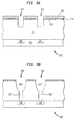
- FIGURE 1A represents a cross sectional view of a stacked semiconductor structure 100.
- Stacked semiconductor structure 100 includes a semiconductor substrate 118, an underlying conductive layer 116 overlaid with a layer of insulator 101.
- a plurality of adjacent via holes 104 used to electrically interconnect various coplanar conductive layers is formed by dual damascene technique as described above.
- the overlying metal lithography is performed after via holes 104 have been formed in insulator 101.
- Via holes 104 may be sized larger than the actual contact area of underlying metallization layer 116 in order to assure proper alignment of via holes 104 to the underlying metallization layer 116.
- a layer of anti-reflective coating 113 (known in the art and referred hereinafter as ARC) is conventionally deposited upon the upper surface of the layer of insulator 101.
- the ARC deposition operation results in a layer of ARC residue 114 unavoidably deposited in via holes 104 to a height approximately a distance "t" above the upper surface of conductive layer 116.
- a layer of metal lithography photoresist is then conventionally deposited upon the upper surface of ARC layer 113.
- the photoresist is subsequently developed and removed by a conventional photoresist strip process to form the metallization resist pattern 102.
- ARC material 114 within via holes 104 is substantially unaffected by the metallization photoresist strip operation.
- ARC layer 113 is removed by exposing the stacked semiconductor structure 100 to a first etch process designed to break through organic ARC layer 113. This first break through etch is followed by a second anisotropic etch designed to create a trench 115 in the insulator 101 into which a metal 116 or other conductive material is subsequently deposited.
- ARC residue 117 remaining within via holes 104 react with various etch by-products to form a sidewall structure.
- the sidewall structure formed substantially inhibits the action of both the first ARC break through etch and the second oxide etch used to form trenches 115 resulting in what is referred to in the art as a fence 218.
- Fence 218 is generally substantially the same height "t" as the ARC residue remaining within the via hole 104 as discussed above.
- the overlying metallization and associated vias are formed substantially simultaneously by depositing metal 116 within trenches 115 by a metal deposition process (sputtering process, for example) followed by metal reflow.
- metal deposition process sputtering process, for example
- metal reflow is highly dependent upon the surface geometry of the surface onto which the metal is deposited.
- the presence of fence 218 within via holes 104 disrupts the flow of metal 116 thereby preventing a smooth flow of metal 116 into via holes 104. This disruption of the flow of metal into via holes 104 may result in the formation of voids 117 within via holes 104, the presence of which substantially increases the electrical contact resistance of the vias.
- the presence of the metal voids 117 may also present unacceptable reliability problems since all the current flowing through each via must be carried by the unvoided metalized portions of the via. High current densities through the unvoided portions of the via may result in electromigration of the via metal. Electromigration of the via metal may result in long term unacceptable Failure In Time (FIT) rates. In some instances, fences 218 may cause the formation of an electrical open by preventing sufficient metal flow into via hole 104.
- FIT Failure In Time
- an additional problem associated with the conventional dual damascene technique relates to the practice of oversizing the vias 104 in the attempt to properly align to the underlying conductive layer 116.
- oversizing vias 104 may result in a reduced thickness "d 1 " of insulator 101(otherwise referred to as interspacing) electrically and physically separating adjacent vias 104.
- This reduced thickness "d 1 " may result in electrical breakdown or electrical current leakage between vias 104 which may result in potential catastrophic temperature related failures that are difficult to screen out in post manufacturing testing.
- Reliability failures evident after only substantial accelerated high temperature reliability testing may also be present due to the small distance between regions of high current densities such as via holes 104 exacerbated by the presence of fences 218 as discussed above.
- FIG. 1C shows a top view of the surface of stacked semiconductor structure 100 along a cross sectional slice "b" of Figure 1B illustrating the proximity of vias 104.
- the proximity of vias 104 may result in significant manufacturing or long term reliability problems related to the various defects described above.
- the present invention relates to semiconductor devices and more particularly, to an improved method of performing a dual damascene etch with self aligned vias through a layer stack disposed above a substrate.
- the layer stack includes an underlying conductive layer and an insulating layer disposed above the underlying conductive layer.
- the method includes the following operative steps. A layer of hard resist is deposited upon a top surface of the insulating layer patterned such that a first opening in the hard resist layer is positioned over the underlying device layer.
- the hard resist layer is composed of silicon oxynitride.
- a layer of soft resist is deposited upon a top surface of the hard resist, the soft resist having a second opening smaller than and aligned to the first opening in said hard resist.
- a trench as defined by the second opening is then formed in the top surface of the insulating layer positioned over and separated from the underlying device layer by insulating material at a bottom of the trench.
- the soft resist is then removed without substantially affecting the hard resist.
- the via is formed by etching through the insulator material at the bottom of the trench down to the underlying device layer.
- a method of forming a via configured for connecting an underlying device layer and an overlying conductor of a layer stack, the overlying conductor configured to be disposed in a trench formed in an insulating layer and spaced apart from the underlying device layer by insulating material at a bottom of the trench includes the following operative steps. Firstly, depositing a hard mask layer over the top surface of said insulating layer, the hard mask having a first opening corresponding to the position of the trench to be formed. Next, depositing a soft mask layer on top of the hard mask layer, the soft mask layer having a second opening corresponding to the location of the via to be formed. Finally, forming the via by etching through the insulating material at the bottom of the trench down to at least the underlying device layer.
- the invention relates to the formation of forming mult-level coplanar metal/insulator films for use in integrated circuits (ICs).
- ICs include, for example, random access memories (RAMs) such as dynamic RAMs (DRAMs), synchronous DRAMs (SDRAMs), or a read only memory (ROM).
- RAMs random access memories
- DRAMs dynamic RAMs
- SDRAMs synchronous DRAMs
- ROM read only memory
- Other ICs such as application specific ICs (ASICs), merged DRAM-logic circuits (embedded DRAMs), or other logic circuits are also useful.
- ASICs application specific ICs
- merged DRAM-logic circuits embedded DRAMs
- other logic circuits are also useful.
- ICs are formed on the wafer in parallel. After processing is finished the wafer is diced to separate the ICs to individual chips. The chips are then packaged, resulting in a final product that is used in, for example, consumer products such as computer systems, cellular phones, personal digital assistants (PDAs), and other electronic products.
- PDAs personal digital assistants
- an improved method for multi-level coplanar metal/insulator films having self aligned vias is provided.
- a dual damascene technique is used which incorporates a first hard mask to form overlying metallization trenches and a soft resist mask to form self aligned vias which electrically connect the overlying metallization layer to an underlying device layer.
- a via is formed through an insulator layer to an underlying device layer using a dual damascene etch with a hard mask composed of silicon oxynitride.
- the hard mask includes a first opening suitable for the formation of the abovemention metallization trenches.
- a soft resist mask is then deposited upon the hard resist mask.
- the soft resist mask includes a second opening smaller than and aligned with the first opening of the hard mask. The second opening is aligned to the underlying conductive layer and is used to form a first trench extending at least about midway to the underlying conductive layer. After formation of the first trench, the soft resist layer is removed without substantially affecting the first hard layer.
- a second anisotropic etch then forms a second trench having a first portion integrally formed with a second portion.
- the first portion extends from the bottom of the first trench to at least the underlying conductive layer and is suitable for forming the via interconnect.
- the second portion is defined by the first opening of the hard mask and is suitable for receiving deposited metal to form the overlying metalization layer.
- the via thus formed is free of any fences since no photoresist or ARC is deposited upon the surface of the semiconductor stacked structure after formation of the first trench. Additionally, since the hard mask is used to define the external configuration of the via, the distance between the vias can be readily controlled.
- Figure 2 illustrates a cross sectional view of a stacked semiconductor structure 200 having an insulator layer 201 overlaying a substrate 218 which includes an underlying conductive layer 216 in accordance with one embodiment of the present invention.
- the stacked semiconductor structure 200 may, for example, represent a stacked semiconductor structure employed to fabricate a conventional transistor such as an n FET or p FET (field effect transistor).
- Insulator layer 201 may be deposited on the substrate 218 of a pre-determined conductivity type. Chemical vapor deposition (CVD) or a similar technique may be employed to deposit insulator 201, which typically includes planarized silicon dioxide, such as TEOS, a glass material such as reflowed phosphosilicate glass, or a polymer like polyimide.
- CVD chemical vapor deposition
- insulator layer 201 is formed over previously defined substrate 218, which includes previously defined conductive layer 216.
- the conductive layer 216 may be a portion of an underlying metallization layer.
- the conductive layer 216 may represent a highly doped silicon layer, a conductive metal such as tungsten, or a portion of any type of active device such as, for example, the source or drain region of a transistor.
- the insulator layer 216 may have a thickness in the range of 0.9 micron to about 2.0 microns.
- insulator layer 201 has an upper surface 202 upon which a hard resist layer 215 has been deposited by any technique known to those of ordinary skill in the art.
- the hard resist may have a thickness of about 1000 ⁇ and may be composed of silicon nitride or, in a preferred embodiment, silicon oxynitride.
- the formation of a first opening 217 located above the underlying conductive layer is accomplished by conventional photolithographic techniques well known to those skilled in the art. In one embodiment, such a method of forming first opening 217 is referred to as reactive ion etching (referred to as RIE) utilizing N 2 as an etchant gas.
- RIE reactive ion etching
- ARC organic anti-reflective coating
- ARC organic anti-reflective coating
- use of silicon oxynitride for hard mask 215 eliminates the need for use of ARC.
- silicon nitride or any other appropriate compound for hard mask 215 may require the additional step or steps related to ARC deposition and removal.
- a soft resist layer 220 of about 1000 ⁇ thickness is deposited upon hard resist layer 215 using convention deposition processes and procedures as shown in Figure 4.
- the soft resist layer 220 is patterned utilizing conventional photolithographic processes and procedures to include a second opening 219 smaller than and aligned to first opening 217 of hard mask 215 as shown in Figure 4.
- the second opening 219 is disposed and sized to form a first trench 224 by a first anisotropic etch which removes sufficient insulator material from insulator layer 201 to form first trench 224 as shown in Figure 5A.
- a first anisotropic etch which removes sufficient insulator material from insulator layer 201 to form first trench 224 as shown in Figure 5A.
- One such method of removing insulator material is by way of an RIE etch, as described above, using for example, Ar, C 4 F 8 , CO and/or O 2 as reactive gases.
- first trench 224 may have its bottom extend to a point about midway between upper surface 202 and underlying conductive layer 216. In another embodiment, first trench 224 may have its bottom extend to a point substantially near or extending to underlying conductive layer 216.
- first opening 217 may be used to form trenches suitably disposed to ultimately form the overlying metallization layer. Since no ARC or photoresist is deposited after the formation of first trench 224, there is no possibility of the formation of the aforementioned fences and the problems associated therewith.
- a second anisotropic etch may be used to form a second trench 204 having a first portion 204' and a second portion 204'' wherein first portion 204' extends substantially to underlying conductive layer 216 while second portion 204'' is arranged to form the desired overlying metallization pattern.
- underlying conductive layer 216 may be used as an etch stop whereby the second anisotropic etch process is halted once a pre-determined amount of the constituent material forming underlying conductive layer is evident in the plasma used in the second anisotropic etch process.
- the overlying metallization layer is ready to be formed by depositing a metal 250 by any appropriate metallization technique.
- Metallization techniques are well known in the art and described, for example in VLSI technology, 2nd Edition, S.M. Sze 1988 McGraw-Hill Publishing Company. Suitable metals and alloys for forming the metallization layer include, for example, aluminum, copper, nickel, molybdenum, tungsten, platinum, tantalum disilicide, titanium disilicide, as well as other alloys of these materials. Aluminum, aluminum alloys such as aluminum silicon, copper, and tungsten are often the materials of choice for interconnection metallization.
- the metals may be deposited by known techniques such as chemical vapor deposition (CVD), physical vapor deposition (PVD), or low pressure chemical vapor deposition (LPCVD).
- CVD chemical vapor deposition
- PVD physical vapor deposition
- LPCVD low pressure chemical vapor deposition
- CVD, PVD and LPCVD The selection of particular equipment and process parameters for CVD, PVD and LPCVD is within the ability one skilled in the art of semiconductor processing.
- Deposition of the metal (usually in blanket fashion over the entire surface of the stacked semiconductor structure 200) fills first portions 204' and second portion 204'' of trench 204 thereby substantially simultaneously creating the overlying metallization layer and the vias interconnecting the overlying metalization layer and the underlying conductive layer 216.
- first and second anisotropic etch is related by the extent that first trench 224 is etched into insulator layer 201.
- first anisotropic etch forms extends first trench 224 to a point proximate to the position of underlying conductive layer 216, then the resulting second anisotropic etch will typically be of shorter duration since less insulator material must be etched resulting in a modified first portion 204' and second portion 204'', respectively.
- This ability to substantially modify the form and structures formed simply by increasing or decreasing the applied etch times offers substantial advantages over more conventional processes.
- FIGURE 7 is an illustrative top view of the stacked semiconductor structure as shown in FIGURE 6 showing the relative positions of vias in relation to the insulative interspacing regions.
- the shape of vias formed coincide with the insulative interspacing regions 201 defined by hard mask 215, thus eliminating the encroachment problem so evident with conventional dual damascene techniques.
- the ability to place vias 204 as illustrated, improves the ability of the designer to route and place integrated circuit interconnections by reducing the problems associated with encroachment of the insulative interspacing regions 201 as evidenced by the increased inter-via spacing d 2 .
- FIGURE 8 The formation of multi-level coplanar metal/insulator films using dual damascene techniques using self aligned vias is detailed in the flowchart illustrated by FIGURE 8 may include the following operative steps.
- a substrate with a layer stack disposed above the substrate is provided.
- the layer stack includes an underlying device layer and an insulating layer disposed above said underlying device layer.
- the substrate is shown as substrate 218 and the underlying device layer is shown as conductive layer 216.
- Insulator layer 201 is shown disposed above the substrate 218 and the underlying conductive layer 216.
- step 815 a layer of hard resist is deposited upon the upper surface of the layer stack having a first opening patterned to define an overlying metallization layer, the first opening being positioned substantially above the underlying device layer.
- the layer of hard resist is shown as hard resist 215 and the opening is shown as first opening 217.
- a layer of soft resist is deposited on the layer of hard resist, the soft resist includes a second opening smaller than and aligned with the first opening, the second opening being for forming a via interconnection to the underlying conductive layer.
- the soft resist mask is shown as soft resist mask 220 and its associated opening is shown as second opening 222.
- a first trench is formed extending to a point about midway through the insulator layer.
- the first trench 224 is substantially aligned to the underlying conductive layer 216 and extends to about midway through insulator layer 201. In some cases, however, it is permissible, and even desirable, to extend first trench 224, to a point near or extending to underlying conducive layer 216.
- a second anisotropic etch is performed to form a second trench after removal of the soft resist layer without substantially affecting the hard resist layer.
- the second anisotropic etch uses the underlying conductive layer as an etchstop forming the structures as illustrated in Figure 5B.
- step 835 the hard resist layer is removed and a metal or other conductive material is deposited within the aforementioned trench substantially simultaneously forming both the overlying metallization layers and the associated via interconnects to the underlying conductive layer.
- Another advantage of the invention relates to the fact that the ultimate shape of the vias substantially conform to the boundaries formed by the insulative interspacing regions. This conformity allows closer spacing of vias without the problems heretofore associated with conventional damascene techniques.
Abstract
Description
Claims (24)
Applications Claiming Priority (2)
| Application Number | Priority Date | Filing Date | Title |
|---|---|---|---|
| US93914997A | 1997-09-29 | 1997-09-29 | |
| US939149 | 1997-09-29 |
Publications (2)
| Publication Number | Publication Date |
|---|---|
| EP0908945A2 true EP0908945A2 (en) | 1999-04-14 |
| EP0908945A3 EP0908945A3 (en) | 2000-09-27 |
Family
ID=25472627
Family Applications (1)
| Application Number | Title | Priority Date | Filing Date |
|---|---|---|---|
| EP98113442A Withdrawn EP0908945A3 (en) | 1997-09-29 | 1998-07-18 | Dual damascene with self aligned via interconnects |
Country Status (5)
| Country | Link |
|---|---|
| EP (1) | EP0908945A3 (en) |
| JP (1) | JPH11163143A (en) |
| KR (1) | KR100554210B1 (en) |
| CN (1) | CN1146980C (en) |
| TW (1) | TW408434B (en) |
Cited By (9)
| Publication number | Priority date | Publication date | Assignee | Title |
|---|---|---|---|---|
| DE19927284A1 (en) * | 1999-06-15 | 2001-02-08 | Infineon Technologies Ag | Making connection in highly-integrated microelectronic structure forms insulated base, etches opening down to contact area, and subsequently re-insulates, trenches and fills with conductive material |
| US6245669B1 (en) * | 1999-02-05 | 2001-06-12 | Taiwan Semiconductor Manufacturing Company | High selectivity Si-rich SiON etch-stop layer |
| KR100349696B1 (en) * | 1999-06-30 | 2002-08-22 | 주식회사 하이닉스반도체 | Method of forming damascene structure for metal interconnection of semiconductor device using chemical swelling process |
| WO2004003998A1 (en) * | 2002-06-28 | 2004-01-08 | Infineon Technologies Ag | Method for contacting parts of a component integrated into a semiconductor substrate |
| KR100424190B1 (en) * | 1998-12-29 | 2004-06-18 | 주식회사 하이닉스반도체 | Metal wiring formation method of semiconductor device |
| JP2006135362A (en) * | 2006-02-14 | 2006-05-25 | Renesas Technology Corp | Method of manufacturing semiconductor device |
| JP2010153909A (en) * | 2010-03-18 | 2010-07-08 | Renesas Technology Corp | Method of manufacturing semiconductor device |
| CN113363157A (en) * | 2020-03-06 | 2021-09-07 | 华邦电子股份有限公司 | Method for manufacturing semiconductor device |
| US11923246B2 (en) | 2021-09-15 | 2024-03-05 | International Business Machines Corporation | Via CD controllable top via structure |
Families Citing this family (6)
| Publication number | Priority date | Publication date | Assignee | Title |
|---|---|---|---|---|
| JP4094174B2 (en) * | 1999-06-04 | 2008-06-04 | 株式会社ルネサステクノロジ | Manufacturing method of semiconductor device |
| JP5079959B2 (en) * | 1999-08-26 | 2012-11-21 | ブルーワー サイエンス アイ エヌ シー. | Improved packing material for dual damascene process |
| KR100387254B1 (en) * | 2000-12-28 | 2003-06-12 | 주식회사 하이닉스반도체 | Method of manufacturing a metal wiring in a semiconductor device |
| JP4516450B2 (en) | 2005-03-02 | 2010-08-04 | ルネサスエレクトロニクス株式会社 | Manufacturing method of semiconductor device |
| US9349606B2 (en) | 2012-05-02 | 2016-05-24 | Lam Research Corporation | Metal hardmask all in one integrated etch |
| TWI475698B (en) * | 2012-09-05 | 2015-03-01 | Giantplus Technology Co Ltd | A method for preventing a break of indium tin oxide conducting line |
Citations (2)
| Publication number | Priority date | Publication date | Assignee | Title |
|---|---|---|---|---|
| US5173442A (en) * | 1990-07-23 | 1992-12-22 | Microelectronics And Computer Technology Corporation | Methods of forming channels and vias in insulating layers |
| WO1995008840A1 (en) * | 1993-09-20 | 1995-03-30 | The Government Of The United States, Represented By The Secretary Of The Navy | Method of fabricating sub-half-micron trenches and holes |
-
1998
- 1998-07-18 EP EP98113442A patent/EP0908945A3/en not_active Withdrawn
- 1998-07-28 TW TW087112357A patent/TW408434B/en not_active IP Right Cessation
- 1998-09-15 CN CNB98119186XA patent/CN1146980C/en not_active Expired - Fee Related
- 1998-09-23 KR KR1019980039359A patent/KR100554210B1/en not_active IP Right Cessation
- 1998-09-29 JP JP10276131A patent/JPH11163143A/en not_active Withdrawn
Patent Citations (2)
| Publication number | Priority date | Publication date | Assignee | Title |
|---|---|---|---|---|
| US5173442A (en) * | 1990-07-23 | 1992-12-22 | Microelectronics And Computer Technology Corporation | Methods of forming channels and vias in insulating layers |
| WO1995008840A1 (en) * | 1993-09-20 | 1995-03-30 | The Government Of The United States, Represented By The Secretary Of The Navy | Method of fabricating sub-half-micron trenches and holes |
Cited By (12)
| Publication number | Priority date | Publication date | Assignee | Title |
|---|---|---|---|---|
| KR100424190B1 (en) * | 1998-12-29 | 2004-06-18 | 주식회사 하이닉스반도체 | Metal wiring formation method of semiconductor device |
| US6245669B1 (en) * | 1999-02-05 | 2001-06-12 | Taiwan Semiconductor Manufacturing Company | High selectivity Si-rich SiON etch-stop layer |
| DE19927284A1 (en) * | 1999-06-15 | 2001-02-08 | Infineon Technologies Ag | Making connection in highly-integrated microelectronic structure forms insulated base, etches opening down to contact area, and subsequently re-insulates, trenches and fills with conductive material |
| DE19927284C2 (en) * | 1999-06-15 | 2002-01-10 | Infineon Technologies Ag | Method for producing an electrically conductive connection in a microelectronic structure |
| KR100349696B1 (en) * | 1999-06-30 | 2002-08-22 | 주식회사 하이닉스반도체 | Method of forming damascene structure for metal interconnection of semiconductor device using chemical swelling process |
| WO2004003998A1 (en) * | 2002-06-28 | 2004-01-08 | Infineon Technologies Ag | Method for contacting parts of a component integrated into a semiconductor substrate |
| US7396749B2 (en) | 2002-06-28 | 2008-07-08 | Infineon Technologies Ag | Method for contacting parts of a component integrated into a semiconductor substrate |
| JP2006135362A (en) * | 2006-02-14 | 2006-05-25 | Renesas Technology Corp | Method of manufacturing semiconductor device |
| JP2010153909A (en) * | 2010-03-18 | 2010-07-08 | Renesas Technology Corp | Method of manufacturing semiconductor device |
| CN113363157A (en) * | 2020-03-06 | 2021-09-07 | 华邦电子股份有限公司 | Method for manufacturing semiconductor device |
| CN113363157B (en) * | 2020-03-06 | 2023-12-08 | 华邦电子股份有限公司 | Method for manufacturing semiconductor device |
| US11923246B2 (en) | 2021-09-15 | 2024-03-05 | International Business Machines Corporation | Via CD controllable top via structure |
Also Published As
| Publication number | Publication date |
|---|---|
| CN1146980C (en) | 2004-04-21 |
| KR19990030048A (en) | 1999-04-26 |
| TW408434B (en) | 2000-10-11 |
| CN1215915A (en) | 1999-05-05 |
| JPH11163143A (en) | 1999-06-18 |
| KR100554210B1 (en) | 2006-04-21 |
| EP0908945A3 (en) | 2000-09-27 |
Similar Documents
| Publication | Publication Date | Title |
|---|---|---|
| US8461692B2 (en) | Semiconductor device structures including damascene trenches with conductive structures and related method | |
| US6103629A (en) | Self-aligned interconnect using high selectivity metal pillars and a via exclusion mask | |
| EP0176010B1 (en) | Integrated circuit fabrication process and device | |
| US4917759A (en) | Method for forming self-aligned vias in multi-level metal integrated circuits | |
| US7611991B2 (en) | Technique for increasing adhesion of metallization layers by providing dummy vias | |
| US7494915B2 (en) | Back end interconnect with a shaped interface | |
| US5434451A (en) | Tungsten liner process for simultaneous formation of integral contact studs and interconnect lines | |
| US6265313B1 (en) | Method of manufacturing copper interconnect | |
| US7056823B2 (en) | Backend metallization method and device obtained therefrom | |
| EP0908945A2 (en) | Dual damascene with self aligned via interconnects | |
| US6191484B1 (en) | Method of forming planarized multilevel metallization in an integrated circuit | |
| US6348734B1 (en) | Self-aligned copper interconnect architecture with enhanced copper diffusion barrier | |
| US6399495B1 (en) | Copper interconnections for metal-insulator-metal capacitor in mixed mode signal process | |
| US6309958B1 (en) | Semiconductor device and method of manufacturing the same | |
| US20050116342A1 (en) | Device interconnection | |
| US5231055A (en) | Method of forming composite interconnect system | |
| EP0248668A2 (en) | Process for fabricating multilevel metal integrated circuits and structures produced thereby | |
| US6274486B1 (en) | Metal contact and process | |
| EP0926721A2 (en) | Dual damascene with bond pads | |
| US20070141842A1 (en) | Method of Manufacturing Semiconductor Device | |
| US6200890B1 (en) | Method of fabricating copper damascene | |
| US20090321946A1 (en) | Process for fabricating an integrated electronic circuit incorporating a process requiring a voltage threshold between a metal layer and a substrate | |
| US6413872B1 (en) | Method op optimizing vias between conductive layers in an integrated circuit structure | |
| US6396151B1 (en) | Partially-overlapped interconnect structure and method of making | |
| JPH0766202A (en) | Manufacture of semiconductor device |
Legal Events
| Date | Code | Title | Description |
|---|---|---|---|
| PUAI | Public reference made under article 153(3) epc to a published international application that has entered the european phase |
Free format text: ORIGINAL CODE: 0009012 |
|
| AK | Designated contracting states |
Kind code of ref document: A2 Designated state(s): DE FR GB IE IT NL |
|
| AX | Request for extension of the european patent |
Free format text: AL;LT;LV;MK;RO;SI |
|
| PUAL | Search report despatched |
Free format text: ORIGINAL CODE: 0009013 |
|
| AK | Designated contracting states |
Kind code of ref document: A3 Designated state(s): AT BE CH CY DE DK ES FI FR GB GR IE IT LI LU MC NL PT SE |
|
| AX | Request for extension of the european patent |
Free format text: AL;LT;LV;MK;RO;SI |
|
| 17P | Request for examination filed |
Effective date: 20001213 |
|
| AKX | Designation fees paid |
Free format text: DE FR GB IE IT NL |
|
| RAP1 | Party data changed (applicant data changed or rights of an application transferred) |
Owner name: INFINEON TECHNOLOGIES AG |
|
| 17Q | First examination report despatched |
Effective date: 20030929 |
|
| REG | Reference to a national code |
Ref country code: HK Ref legal event code: WD Ref document number: 1017141 Country of ref document: HK |
|
| STAA | Information on the status of an ep patent application or granted ep patent |
Free format text: STATUS: THE APPLICATION IS DEEMED TO BE WITHDRAWN |
|
| 18D | Application deemed to be withdrawn |
Effective date: 20060915 |