EP0903590A1 - Radiation detection device and method of producing the same - Google Patents
Radiation detection device and method of producing the same Download PDFInfo
- Publication number
- EP0903590A1 EP0903590A1 EP98902186A EP98902186A EP0903590A1 EP 0903590 A1 EP0903590 A1 EP 0903590A1 EP 98902186 A EP98902186 A EP 98902186A EP 98902186 A EP98902186 A EP 98902186A EP 0903590 A1 EP0903590 A1 EP 0903590A1
- Authority
- EP
- European Patent Office
- Prior art keywords
- light
- resin
- receiving
- protective film
- film
- Prior art date
- Legal status (The legal status is an assumption and is not a legal conclusion. Google has not performed a legal analysis and makes no representation as to the accuracy of the status listed.)
- Granted
Links
Images


Classifications
-
- G—PHYSICS
- G01—MEASURING; TESTING
- G01T—MEASUREMENT OF NUCLEAR OR X-RADIATION
- G01T1/00—Measuring X-radiation, gamma radiation, corpuscular radiation, or cosmic radiation
- G01T1/16—Measuring radiation intensity
- G01T1/20—Measuring radiation intensity with scintillation detectors
-
- G—PHYSICS
- G01—MEASURING; TESTING
- G01T—MEASUREMENT OF NUCLEAR OR X-RADIATION
- G01T1/00—Measuring X-radiation, gamma radiation, corpuscular radiation, or cosmic radiation
- G01T1/16—Measuring radiation intensity
- G01T1/20—Measuring radiation intensity with scintillation detectors
- G01T1/2018—Scintillation-photodiode combinations
- G01T1/20188—Auxiliary details, e.g. casings or cooling
- G01T1/20189—Damping or insulation against damage, e.g. caused by heat or pressure
Definitions
- the present invention relates to a radiation detection device; and, in particular, to a radiation detection device having a light-receiving portion with a large area, which is used for medical X-raying and the like.
- X-ray sensitive films have conventionally been used for medical and industrial X-raying
- radiation imaging systems using a radiation detection device are becoming pervasive due to their convenience and the storability of their photographed results.
- a radiation imaging system uses a radiation detection device having a plurality of pixels so as to acquire, as an electric signal, two-dimensional image data formed by a radiation, and processes thus obtained signal with a processing unit, so as to display it on a monitor.
- a typical radiation detection device is configured such that a scintillator is disposed on one- or two-dimensionally arranged photodetectors so as to convert the incident radiation into light, which is then detected.
- CsI a typical scintillator material
- a typical scintillator material is a hygroscopic material which dissolves by absorbing vapor (moisture) in the air.
- characteristics of the scintillator such as resolution in particular, have disadvantageously deteriorated.
- a radiation detection device having a structure for protecting the scintillator against moisture is the technique disclosed in Japanese Patent Application Laid-Open No. 5-196742.
- a water-impermeable moisture-proof barrier is formed on the upper side of the scintillator layer, thereby protecting the scintillator against moisture.
- the above-mentioned technique discloses a method of making a moisture seal layer for the moisture-proof barrier in which a silicone potting material or the like is coated on the scintillator layer in a liquid state or coated inside a window member disposed on the light-receiving surface side of the radiation detection device and then the window member is disposed on the scintillator layer before the moisture seal layer is dried, thereby fixing the moisture seal layer.
- a silicone potting material or the like is coated on the scintillator layer in a liquid state or coated inside a window member disposed on the light-receiving surface side of the radiation detection device and then the window member is disposed on the scintillator layer before the moisture seal layer is dried, thereby fixing the moisture seal layer.
- this method it is hard to uniformly form the moisture seal layer on a scintillator layer having an irregular surface form, whereby adhesion may deteriorate. This phenomenon tends to occur in radiation detection devices having a large area, in particular.
- the radiation detection device of the present invention comprises: (1) a light-receiving device array in which a plurality of light-receiving devices are one- or two-dimensionally arranged on a substrate to form a light-receiving portion, and a plurality of bonding pads electrically connected to the light-receiving devices in respective rows or columns of the light-receiving portion are disposed outside the light-receiving portion; (2) a scintillator layer, deposited on the light-receiving devices of the light-receiving portion, for converting a radiation into visible light; (3) one or a plurality of resin frames made of a resin each formed like a closed frame separating an area formed with the scintillator layer on the light-receiving device array and an area in which the bonding pads are arranged from each other; and (4) a radiation-transmittable, moisture-resistant protective film, constituted by a multilayer film made of at least two layers including an organic film and an
- the incident radiation is converted into visible light by the scintillator layer.
- the resulting visible light image is detected by the one- or two-dimensionally arranged light-receiving devices, an image electric signal corresponding to the incident radiation image is obtained.
- the scintillator layer has a characteristic of deteriorating by absorbing moisture. In the present invention, however, since the scintillator layer is covered with the moisture-resistant protective film, which is in close contact with the light-receiving device array with the aid of the resin frame, the scintillator layer is completely hermetically sealed so as to be isolated from the external atmosphere, thus being protected against vapor in the air. Further, the bonding pad portion for connection with an external circuit is exposed.
- the resin frame is formed like a rectangle surrounding the scintillator layer or one or a plurality of rectangles respectively surrounding their corresponding bonding pad areas.
- a coating resin for covering an edge of the moisture-resistant protective film along the resin frame may further be provided.
- the edge of the moisture-resistant protective film is held between the resin frame and coating resin from the upper and lower sides, so as to be firmly bonded.
- the method of making a radiation detection device in accordance with the present invention comprises: (1) a first step of forming a light-receiving portion by one- or two-dimensionally arranging a plurality of light-receiving devices on a substrate, and depositing a scintillator layer for converting a radiation into visible light on the light-receiving devices of the light-receiving portion of a light-receiving device array in which a plurality of bonding pads electrically connected to the light-receiving devices in respective rows or columns of the light-receiving portion are disposed outside the light-receiving portion; (2) a second step of forming with a resin, on the light-receiving device array, one or a plurality of resin frames each formed like a closed frame separating the scintillator layer and a bonding pad portion from each other; (3) a third step of forming a radiation-transmittable first organic film enveloping the light-receiving device
- the adhesion between the scintillator layer and the organic film improves, thereby forming a uniform film.
- the moisture-resistant protective film is removed from the bonding pad portion after being formed, the bonding pad portion is securely exposed.
- the resin frame formed under the protective film adds a margin to the cut-in depth of a cutter when cutting the protective film. Further, the resin frame brings edges of the protective film into close contact with the substrate, thereby assuring the sealing.
- a sixth step of covering and bonding an edge of the moisture-resistant protective film along the resin frame with a resin may further be provided after the fifth step.
- the edge of the moisture-resistant protective film is held between the resin frame and this resin so as to be firmly bonded.
- Fig. 1 is a top plan view showing an embodiment of the present invention
- Fig. 2 is an enlarged sectional view of its outer peripheral portion taken along the line A-A.
- each light-receiving device 2 is constituted by a photodiode (PD) made of amorphous silicon or a thin-film transistor (TFT).
- PD photodiode
- TFT thin-film transistor
- a plurality of bonding pads 4 for taking out signals to an external circuit are disposed along outer peripheral sides, e.g., two adjacent sides, of the substrate 1 and are electrically connected to their corresponding plurality of light-receiving devices 2 via the signal lines 3.
- An insulating passivation film 5 is formed on the light-receiving devices 2 and signal lines 3.
- silicon nitride or silicon oxide is preferably used.
- the bonding pads 4 are exposed for connection with the external circuit.
- this substrate and the circuit portion on the substrate are referred to as a light-receiving device array 6.
- various materials can be used for the scintillator 7, Tl-doped CsI or the like, which has a favorable emission efficiency, is preferable.
- a resin frame 8 formed like an elongated frame from a resin is disposed at a position inside the bonding pads, so as to surround the outer periphery of the light-receiving device array 6.
- Laminated on the scintillator 7 inside the frame of the resin frame 8 are a first organic film 9, an inorganic film 10, and a second organic film 11, each transmitting X-rays therethrough but blocking vapor, thereby forming a protective film 12.
- a poly-para-xylylene resin manufactured by Three Bond Co., Ltd.; trade name: Parylene
- poly-para-chloroxylylene manufactured by the same company; trade name: Parylene C
- the coating film made of Parylene has excellent characteristics suitable for the organic films 9, 11 in that, for example, it transmits therethrough only a very small amount of vapor and gasses, has high water repellency and chemical resistance, exhibits excellent electrical insulation even in a thin film, and is transparent to radiation and visible light.
- the details of the coating with Parylene are described in Three Bond Technical News (issued September 23, 1992), and their characteristics will be noted here.
- Parylene can be coated by chemical vapor deposition (CVD) method in which it is vapor-deposited on a support in vacuum as with the vacuum vapor deposition of metals.
- This method comprises a step of thermally decomposing p-xylene, which is a raw material, and rapidly cooling the resulting product in an organic solvent such as toluene or benzene, so as to yield di-para-xylylene which is known as dimer; a step of thermally decomposing this dimer so as to generate a stable radical para-xylylene gas; and a step of causing thus generated gas to be absorbed and polymerized on a material so as to form a poly-para-xylylene film having a molecular weight of about 500,000 by polymerization.
- CVD chemical vapor deposition
- the pressure at the time of Parylene vapor deposition is 0.1 to 0.2 torr, which is higher than the pressure in the case of metal vacuum vapor deposition, 0.001 torr.
- a monomolecular film covers the whole material to be coated, and then Parylene is vapor-deposited thereon. Consequently, a thin film having a thickness as small as 0.2 ⁇ m can be formed with a uniform thickness in the state free of pinholes. Therefore, the coating on acute angle portions, edge portions, and narrow gaps of the order of microns, which has been impossible in the liquid form, can be effected.
- the coating can be effected at a temperature close to room temperature, without needing heat treatment and the like at the time of coating. As a consequence, mechanical stress or thermal distortion accompanying hardening would not occur, and the coating is excellent in stability as well. Further, coating is possible with respect to almost any solid material.
- the inorganic film 10 various materials such as those transparent, opaque, or reflective to visible light can be used as long as they can transmit X-rays therethrough. Oxidized films of Si, Ti, and Cr, and metal thin films of gold, silver, aluminum, and the like can be used. In particular, a film reflective to visible light is preferably used, since it is effective in preventing fluorescence generated in the scintillator 7 from leaking out, thereby enhancing sensitivity.
- Al which is easy to shape will be explained. Though Al itself is likely to corrode in the air, the inorganic film 10 is protected against corrosion since it is held between the first organic film 9 and the second organic film 11.
- this protective film 12 is formed by the above-mentioned Parylene coating, since it is formed by CVD method, it is formed such as to cover the whole surface of the light-receiving device array 6. Therefore, in order to expose the bonding pads 4, it is necessary that the protective film 12 formed by the Parylene coating be cut inside the bonding pads 4, and the outer part of the protective film 12 be removed. As will be mentioned later, when the protective film 12 is cut near substantially the center of the frame portion of the resin frame 8, the outer peripheral portion of the protective film 12 would be fixed by the resin frame 8, whereby the protective film 12 can be prevented from peeling off from the outer peripheral portion. Further, the outer peripheral portion of the protective film 12, together with the resin frame 8 thereunder, is coated with a coating resin 13.
- a resin which favorably adheres to the protective film 12 and resin frame 8 such as WORLD ROCK No. 801-SET2 (70,000 cP type) manufactured by Kyoritsu Chemical Industries Co., Ltd., which is an acrylic adhesive, for example, is preferably used.
- This resin adhesive is hardened in about 20 seconds upon UV irradiation at 100 mW/cm 2 .
- hardened coating film is soft but has a sufficient strength, is excellent in resistances to moisture, water, galvanic corrosion, and migration, favorably adheres to various materials such as glass, plastics, and the like in particular, and thus has favorable characteristics as the coating resin 13.
- the same silicone resin as the resin frame 8 may be used.
- the same acrylic adhesive as the coating resin 13 may be used for the resin frame 8.
- the resin frame 8 is formed like an elongated frame having a width of 1 mm and a height of 0.6 mm on the passivation film 5 inside the bonding pads 4 along the outer perimeter of the light-receiving portion.
- an automatic X-Y coating apparatus such as AutoShooter-3 manufactured by Iwashita Engineering Ltd. is preferably used.
- the surface of the resin frame 8 is subjected to a rough-surface treatment. Examples of the rough-surface treatment include scoring and forming a number of small depressions on the surface.
- CsI which forms the layer of scintillator 7 is highly hygroscopic, so that it dissolves by absorbing vapor in the air when left exposed.
- CVD method is used for enveloping the whole substrate with Parylene at a thickness of 10 ⁇ m, thereby forming the first organic film 9.
- Parylene intrudes into these narrow gaps to some extent, whereby the first organic film 9 comes into close contact with the scintillator layer 7.
- the Parylene coating yields a precision thin film coating with a uniform thickness on the layer of scintillator 7 having irregularities. Since Parylene can be formed by CVD at a lower vacuum than in the case with the metal vapor deposition and at normal temperature as mentioned above, it can be processed easily.
- an Al film having a thickness of 0.2 ⁇ m is laminated on the surface of the first organic film 9 on the entrance side by vapor deposition method, thus forming the inorganic film 10. Then, by using CVD method again, the surface of the whole substrate is coated with Parylene at a thickness of 10 ⁇ m, thereby forming the second organic film 11 (see Fig. 8). This second organic film 11 prevents the inorganic film 10 from deteriorating due to corrosion.
- the passivation film 5 and the first organic film 9 do not adhere to each other well.
- the resin frame 8 adapted to closely adhere to both of the first organic film 9 and the passivation film 5 is disposed therebetween, the first organic film 9 comes into close contact with the passivation film 5 with the aid of the resin frame 8.
- the coating resin 13 is preferably formed since the protective film 12 including the first organic film 9 would be fixed thereby as being held between the resin frame 8 and the coating resin 13, thus further improving the adhesion of the protective film 12 onto the light-receiving device array 6.
- the scintillator 7 is hermetically sealed with the protective film 12, whereby moisture can securely be prevented from intruding into the scintillator 7, thus making it possible to keep the resolution of device from decreasing due to the deterioration of the scintillator 7 caused by moisture absorption.
- each light-receiving device 2 an electric signal corresponding to the light quantity of the visible light is generated by photoelectric conversion and is stored for a predetermined period of time. Since the light quantity of the visible light corresponds to the dose of the incident X-ray, the electric signal stored in each light-receiving device 2 corresponds to the dose of the incident X-ray, whereby an image signal corresponding to an X-ray image is obtained.
- the image signals stored in the light-receiving devices 2 are sequentially read out from the bonding pads 4 via the signal lines 3, transferred to the outside, and processed in a predetermined processing circuit, whereby the X-ray image can be displayed.
- the protective film 12 having a configuration in which the inorganic film 10 is held between the first and second organic films 9, 11 made of Parylene
- the first organic film 9 and the second organic film 11 may be made of materials different from each other.
- the second organic film 11 per se may be omitted.
- the resin frame 8 and the coating resin 13 are formed on the passivation film 5 outside the part formed with the light-receiving devices 2 if they are located close to each other.
- the positions of the resin frame 8 and coating resin 13 be shifted toward the light-receiving device 2.
- the scintillator 7 is not formed on the whole surface on the light-receiving devices 2 but on the light-receiving devices 2 in the effective screen area excluding the pixels near the bonding pads 4.
- the protective film 12 is formed so as to cover the formed layer of scintillator 7 as a whole and reach the resin frame 8. Thereafter, the protective film 12 is cut along the longitudinal direction of the resin frame 8, the part of the protective film 12 outside the effective screen area is removed, and then the edges of the protective film 12 are coated with the coating resin 13 along the resin frame 8. In this case, since the pixels near the bonding pads 4 are covered with the resin frame 8 and the coating resin 13 or are free of the scintillator 7 on the front side, their sensitivity to the radiation decreases.
- the light-receiving devices 2 constitute a large screen and have a large number of pixels in total, however, the ratio of the ineffective pixels is small and, depending on the configuration of devices, they may yield a merit that manufacturing becomes easier.
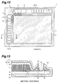
- FIG. 12 is a top plan view of the radiation detection device in accordance with this embodiment
- Fig. 13 is an enlarged sectional view thereof taken along the line B-B. Since the basic configuration of this device is basically the same as that of the embodiment shown in Figs. 1 and 2, only their differences will be explained in the following.
- the protective film 12 is formed on the whole surface of the light-receiving device array 6 on the light-receiving surface side and the rear side, exposing only the bonding pad array 4 portion.
- the resin frame 8 is formed such as to surround the exposed bonding pad array 4 portion, and the coating resin 13 is coated on the resin frame 8 along the boundaries (edges) of the protective film 12. Since the bonding pad 4 portion is securely exposed, and the protective film 12 securely adheres to the light-receiving device array 6 with the aid of the resin frame 8 and coating resin 13, the layer of scintillator 7 is hermetically sealed, whereby it can be prevented from deteriorating due to moisture absorption in this embodiment as well.
- This embodiment is effective in that it can reduce the length of the edge portion acting as a boundary portion which may cause the protective film to peel off, in particular, in the case of CCD or MOS type imaging devices in which the bonding pad portion 4 is small.
- the present invention is also applicable to so-called rear face entrance type radiation detection devices.
- a rear face entrance type radiation detection device can be used as a high-energy radiation detection device.
- a protective film made of Parylene or the like is formed on the scintillator, and the outer periphery of the protective film is bonded to the light-receiving device array with a resin layer, whereby the scintillator layer is hermetically sealed in accordance with the present invention.
- the peeling from the edges of the protective film is prevented from occurring, resistance to moisture would be improved.
- the hermetic sealing will further be improved, thus enhancing the resistance to moisture.
- the protective film is formed and then unnecessary parts thereof are removed, whereby the protective film in a uniform state is formed more easily as compared with the case where the protective film is formed on only necessary parts, while securely exposing the bonding pads. Also, since the protective film penetrates through the gaps among the columnar crystals in the scintillator layer, the adhesion between the protective film and scintillator layer increases. Further, since the thickness of the resin layer provides a cut-in margin for the cutter when cutting, the signal lines for reading out detected signals would not be damaged even when the accuracy of the cutting tool is not enhanced, thereby improving the yield of the product.
- the radiation detection device in accordance with the present invention is applicable to a large-area radiation imaging system used for medical and industrial X-raying in particular. It can be used for chest X-raying or the like in place of X-ray films which are currently in wide use in particular.
Abstract
Description
- The present invention relates to a radiation detection device; and, in particular, to a radiation detection device having a light-receiving portion with a large area, which is used for medical X-raying and the like.
- While X-ray sensitive films have conventionally been used for medical and industrial X-raying, radiation imaging systems using a radiation detection device are becoming pervasive due to their convenience and the storability of their photographed results. Such a radiation imaging system uses a radiation detection device having a plurality of pixels so as to acquire, as an electric signal, two-dimensional image data formed by a radiation, and processes thus obtained signal with a processing unit, so as to display it on a monitor. A typical radiation detection device is configured such that a scintillator is disposed on one- or two-dimensionally arranged photodetectors so as to convert the incident radiation into light, which is then detected.
- CsI, a typical scintillator material, is a hygroscopic material which dissolves by absorbing vapor (moisture) in the air. As a result, characteristics of the scintillator, such as resolution in particular, have disadvantageously deteriorated.
- Known as a radiation detection device having a structure for protecting the scintillator against moisture is the technique disclosed in Japanese Patent Application Laid-Open No. 5-196742. In this technique, a water-impermeable moisture-proof barrier is formed on the upper side of the scintillator layer, thereby protecting the scintillator against moisture.
- In the above-mentioned technique, however, it is hard for the moisture-proof barrier in the outer peripheral portion of the scintillator layer to come into close contact with the substrate of the radiation detection device. In particular, in a radiation detection device having a large area used for chest X-raying or the like, due to its long outer peripheral portion, there is a fear of peeling off the moisture-proof barrier. Hence, the hermetic sealing of the scintillator layer might become incomplete, moisture penetrates into the scintillator layer, it might cause a problem that deteriorates characteristics of the scintillator layer.
- Also, the above-mentioned technique discloses a method of making a moisture seal layer for the moisture-proof barrier in which a silicone potting material or the like is coated on the scintillator layer in a liquid state or coated inside a window member disposed on the light-receiving surface side of the radiation detection device and then the window member is disposed on the scintillator layer before the moisture seal layer is dried, thereby fixing the moisture seal layer. In this method, it is hard to uniformly form the moisture seal layer on a scintillator layer having an irregular surface form, whereby adhesion may deteriorate. This phenomenon tends to occur in radiation detection devices having a large area, in particular.
- In view of the foregoing problems, it is an object of the present invention to provide a radiation detection device having a uniform protective film, which is easy to make, for protecting the scintillator against moisture; and a method of making the same.
- In order to achieve this object, the radiation detection device of the present invention comprises: (1) a light-receiving device array in which a plurality of light-receiving devices are one- or two-dimensionally arranged on a substrate to form a light-receiving portion, and a plurality of bonding pads electrically connected to the light-receiving devices in respective rows or columns of the light-receiving portion are disposed outside the light-receiving portion; (2) a scintillator layer, deposited on the light-receiving devices of the light-receiving portion, for converting a radiation into visible light; (3) one or a plurality of resin frames made of a resin each formed like a closed frame separating an area formed with the scintillator layer on the light-receiving device array and an area in which the bonding pads are arranged from each other; and (4) a radiation-transmittable, moisture-resistant protective film, constituted by a multilayer film made of at least two layers including an organic film and an inorganic film laminated thereon, covering at least the scintillator layer and reaching above the resin frame so as to expose at least the bonding pad portion.
- As a consequence, the incident radiation is converted into visible light by the scintillator layer. As the resulting visible light image is detected by the one- or two-dimensionally arranged light-receiving devices, an image electric signal corresponding to the incident radiation image is obtained. The scintillator layer has a characteristic of deteriorating by absorbing moisture. In the present invention, however, since the scintillator layer is covered with the moisture-resistant protective film, which is in close contact with the light-receiving device array with the aid of the resin frame, the scintillator layer is completely hermetically sealed so as to be isolated from the external atmosphere, thus being protected against vapor in the air. Further, the bonding pad portion for connection with an external circuit is exposed.
- Preferably, the resin frame is formed like a rectangle surrounding the scintillator layer or one or a plurality of rectangles respectively surrounding their corresponding bonding pad areas.
- A coating resin for covering an edge of the moisture-resistant protective film along the resin frame may further be provided. In this case, the edge of the moisture-resistant protective film is held between the resin frame and coating resin from the upper and lower sides, so as to be firmly bonded.
- On the other hand, the method of making a radiation detection device in accordance with the present invention comprises: (1) a first step of forming a light-receiving portion by one- or two-dimensionally arranging a plurality of light-receiving devices on a substrate, and depositing a scintillator layer for converting a radiation into visible light on the light-receiving devices of the light-receiving portion of a light-receiving device array in which a plurality of bonding pads electrically connected to the light-receiving devices in respective rows or columns of the light-receiving portion are disposed outside the light-receiving portion; (2) a second step of forming with a resin, on the light-receiving device array, one or a plurality of resin frames each formed like a closed frame separating the scintillator layer and a bonding pad portion from each other; (3) a third step of forming a radiation-transmittable first organic film enveloping the light-receiving device array as a whole; (4) a fourth step of laminating at least one layer of film including an inorganic film on the first organic film so as to form a radiation-transmittable, moisture-resistant protective film constituted by a multilayer film made of at least two layers; and (5) a fifth step of cutting the moisture-resistant protective film along a longitudinal direction of the resin frame and removing the moisture-resistant protective film on the bonding pad portion so as to expose the bonding pad portion.
- As the first organic film is formed such as to envelope the light-receiving device array as a whole, the adhesion between the scintillator layer and the organic film improves, thereby forming a uniform film. As the moisture-resistant protective film is removed from the bonding pad portion after being formed, the bonding pad portion is securely exposed. The resin frame formed under the protective film adds a margin to the cut-in depth of a cutter when cutting the protective film. Further, the resin frame brings edges of the protective film into close contact with the substrate, thereby assuring the sealing.
- A sixth step of covering and bonding an edge of the moisture-resistant protective film along the resin frame with a resin may further be provided after the fifth step. In this case, the edge of the moisture-resistant protective film is held between the resin frame and this resin so as to be firmly bonded.
-
- Fig. 1 is a top plan view showing an embodiment of the present invention, whereas Fig. 2 is an enlarged sectional view thereof taken along the line A-A;
- Figs. 3 to 11 are views showing manufacturing steps of the embodiment in accordance with Figs. 1 and 2; and
- Fig. 12 is a top plan view showing another embodiment of the present invention, whereas Fig. 13 is an enlarged sectional view thereof taken along the line B-B.
-
- In the following, preferred embodiments of the present invention will be explained with reference to the drawings. To facilitate the comprehension of the explanation, the same reference numerals denote the same parts, where possible, throughout the drawings, and a repeated explanation will be omitted. Also, the dimensions and forms in each drawing are not always identical to those in practice but include parts exaggerated to facilitate understanding.
- Fig. 1 is a top plan view showing an embodiment of the present invention, whereas Fig. 2 is an enlarged sectional view of its outer peripheral portion taken along the line A-A.
- First, the configuration of this embodiment will be explained with reference to Figs. 1 and 2. On an
insulating substrate 1, such as that made of glass, for example, light-receiving devices 2 for effecting photoelectric conversion are arranged two-dimensionally, so as to form a light-receiving portion. Each light-receivingdevice 2 is constituted by a photodiode (PD) made of amorphous silicon or a thin-film transistor (TFT). The light-receiving devices 2 in the respective rows or columns are electrically connected to each other viasignal lines 3 for reading out signals. A plurality ofbonding pads 4 for taking out signals to an external circuit (not shown) are disposed along outer peripheral sides, e.g., two adjacent sides, of thesubstrate 1 and are electrically connected to their corresponding plurality of light-receiving devices 2 via thesignal lines 3. Aninsulating passivation film 5 is formed on the light-receivingdevices 2 andsignal lines 3. For thepassivation film 5, silicon nitride or silicon oxide is preferably used. On the other hand, thebonding pads 4 are exposed for connection with the external circuit. In the following, this substrate and the circuit portion on the substrate are referred to as a light-receivingdevice array 6. - Formed on the light-receiving portion of the light-receiving
device array 6 is ascintillator 7, having a columnar structure, for converting an incident radiation into visible light. Though various materials can be used for thescintillator 7, Tl-doped CsI or the like, which has a favorable emission efficiency, is preferable. Aresin frame 8 formed like an elongated frame from a resin is disposed at a position inside the bonding pads, so as to surround the outer periphery of the light-receivingdevice array 6. As thisresin frame 8, KJR651 or KE4897 manufactured by Shin-Etsu Chemical Co., Ltd., TSE397 manufactured by Toshiba Silicone Co., Ltd., and DYMAX625T manufactured by Sumitomo 3M Ltd., which are silicone resins, and the like are preferably used. This is because they are widely used for surface processing for mechanically and electrically protecting semiconductor devices and exhibit high adhesion to aprotective film 12 formed on the upper side which will be explained later. - Laminated on the
scintillator 7 inside the frame of theresin frame 8 are a firstorganic film 9, aninorganic film 10, and a secondorganic film 11, each transmitting X-rays therethrough but blocking vapor, thereby forming aprotective film 12. - As the first
organic film 9 and the secondorganic film 11, a poly-para-xylylene resin (manufactured by Three Bond Co., Ltd.; trade name: Parylene), such as poly-para-chloroxylylene (manufactured by the same company; trade name: Parylene C) in particular, is preferably used. The coating film made of Parylene has excellent characteristics suitable for theorganic films - Parylene can be coated by chemical vapor deposition (CVD) method in which it is vapor-deposited on a support in vacuum as with the vacuum vapor deposition of metals. This method comprises a step of thermally decomposing p-xylene, which is a raw material, and rapidly cooling the resulting product in an organic solvent such as toluene or benzene, so as to yield di-para-xylylene which is known as dimer; a step of thermally decomposing this dimer so as to generate a stable radical para-xylylene gas; and a step of causing thus generated gas to be absorbed and polymerized on a material so as to form a poly-para-xylylene film having a molecular weight of about 500,000 by polymerization.
- The pressure at the time of Parylene vapor deposition is 0.1 to 0.2 torr, which is higher than the pressure in the case of metal vacuum vapor deposition, 0.001 torr. Upon vapor deposition, a monomolecular film covers the whole material to be coated, and then Parylene is vapor-deposited thereon. Consequently, a thin film having a thickness as small as 0.2 µm can be formed with a uniform thickness in the state free of pinholes. Therefore, the coating on acute angle portions, edge portions, and narrow gaps of the order of microns, which has been impossible in the liquid form, can be effected. Also, the coating can be effected at a temperature close to room temperature, without needing heat treatment and the like at the time of coating. As a consequence, mechanical stress or thermal distortion accompanying hardening would not occur, and the coating is excellent in stability as well. Further, coating is possible with respect to almost any solid material.
- For the
inorganic film 10, various materials such as those transparent, opaque, or reflective to visible light can be used as long as they can transmit X-rays therethrough. Oxidized films of Si, Ti, and Cr, and metal thin films of gold, silver, aluminum, and the like can be used. In particular, a film reflective to visible light is preferably used, since it is effective in preventing fluorescence generated in thescintillator 7 from leaking out, thereby enhancing sensitivity. Here, an example using Al which is easy to shape will be explained. Though Al itself is likely to corrode in the air, theinorganic film 10 is protected against corrosion since it is held between the firstorganic film 9 and the secondorganic film 11. - While this
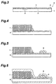
protective film 12 is formed by the above-mentioned Parylene coating, since it is formed by CVD method, it is formed such as to cover the whole surface of the light-receivingdevice array 6. Therefore, in order to expose thebonding pads 4, it is necessary that theprotective film 12 formed by the Parylene coating be cut inside thebonding pads 4, and the outer part of theprotective film 12 be removed. As will be mentioned later, when theprotective film 12 is cut near substantially the center of the frame portion of theresin frame 8, the outer peripheral portion of theprotective film 12 would be fixed by theresin frame 8, whereby theprotective film 12 can be prevented from peeling off from the outer peripheral portion. Further, the outer peripheral portion of theprotective film 12, together with theresin frame 8 thereunder, is coated with acoating resin 13. For thecoating resin 13, a resin which favorably adheres to theprotective film 12 andresin frame 8, such as WORLD ROCK No. 801-SET2 (70,000 cP type) manufactured by Kyoritsu Chemical Industries Co., Ltd., which is an acrylic adhesive, for example, is preferably used. This resin adhesive is hardened in about 20 seconds upon UV irradiation at 100 mW/cm2. Thus hardened coating film is soft but has a sufficient strength, is excellent in resistances to moisture, water, galvanic corrosion, and migration, favorably adheres to various materials such as glass, plastics, and the like in particular, and thus has favorable characteristics as thecoating resin 13. Alternatively, the same silicone resin as theresin frame 8 may be used. Also, the same acrylic adhesive as thecoating resin 13 may be used for theresin frame 8. - The manufacturing process of this embodiment will now be explained with reference to Figs. 3 to 11. As shown in Fig. 4, columnar crystals of Tl-doped CsI are grown according to vapor deposition method by a thickness of 600 µm on the light-receiving surface of the light-receiving
device array 6 shown in Fig. 3, so as to form a layer of thescintillator 7. - On the other hand, as shown in Fig. 5, between the respective outer peripheries of the light-receiving portion and light-receiving device array, the
resin frame 8 is formed like an elongated frame having a width of 1 mm and a height of 0.6 mm on thepassivation film 5 inside thebonding pads 4 along the outer perimeter of the light-receiving portion. For forming this frame, for example, an automatic X-Y coating apparatus such as AutoShooter-3 manufactured by Iwashita Engineering Ltd. is preferably used. At this time, for further improving the adhesion to the firstorganic film 9 formed on the upper side, it will be more preferable if the surface of theresin frame 8 is subjected to a rough-surface treatment. Examples of the rough-surface treatment include scoring and forming a number of small depressions on the surface. - CsI, which forms the layer of
scintillator 7 is highly hygroscopic, so that it dissolves by absorbing vapor in the air when left exposed. In order to prevent this phenomenon from occurring, as shown in Fig. 6, CVD method is used for enveloping the whole substrate with Parylene at a thickness of 10 µm, thereby forming the firstorganic film 9. Though there are gaps among the columnar crystals of CsI, Parylene intrudes into these narrow gaps to some extent, whereby the firstorganic film 9 comes into close contact with thescintillator layer 7. Further, the Parylene coating yields a precision thin film coating with a uniform thickness on the layer ofscintillator 7 having irregularities. Since Parylene can be formed by CVD at a lower vacuum than in the case with the metal vapor deposition and at normal temperature as mentioned above, it can be processed easily. - Further, as shown in Fig. 7, an Al film having a thickness of 0.2 µm is laminated on the surface of the first
organic film 9 on the entrance side by vapor deposition method, thus forming theinorganic film 10. Then, by using CVD method again, the surface of the whole substrate is coated with Parylene at a thickness of 10 µm, thereby forming the second organic film 11 (see Fig. 8). This secondorganic film 11 prevents theinorganic film 10 from deteriorating due to corrosion. - Thus formed
protective film 12 is cut with acutter 14 along the longitudinal direction of the resin frame 8 (see Fig. 9). Since theresin frame 8 forms a protrusion, the cut portion is easily confirmed. Also, since the thickness of theresin frame 8 forms a margin for inserting thecutter 14, there is no fear of thesignal lines 3 under theresin frame 8 being damaged. Hence, the processing becomes easier, thereby improving the yield of the product. Thereafter, from thus cut portion, the parts of theprotective film 12 on the outer side thereof and the rear side of the entrance surface are removed, so as to expose thebonding pads 4 for connection with the external circuit (see Fig. 10). Thereafter, the outer peripheral portion of theprotective film 12 and the exposedresin frame 8 are coated and covered with acoating resin 13, which is then hardened upon UV irradiation (see Fig. 11). - In general, the
passivation film 5 and the firstorganic film 9 do not adhere to each other well. In accordance with the configuration of this embodiment, however, since theresin frame 8 adapted to closely adhere to both of the firstorganic film 9 and thepassivation film 5 is disposed therebetween, the firstorganic film 9 comes into close contact with thepassivation film 5 with the aid of theresin frame 8. Though theprotective film 12 will closely adhere to the light-receivingdevice array 12 with the aid of theresin frame 8 even if thecoating resin 13 is not provided, thecoating resin 13 is preferably formed since theprotective film 12 including the firstorganic film 9 would be fixed thereby as being held between theresin frame 8 and thecoating resin 13, thus further improving the adhesion of theprotective film 12 onto the light-receivingdevice array 6. As a consequence, thescintillator 7 is hermetically sealed with theprotective film 12, whereby moisture can securely be prevented from intruding into thescintillator 7, thus making it possible to keep the resolution of device from decreasing due to the deterioration of thescintillator 7 caused by moisture absorption. - The operation of this embodiment will now be explained with reference to Figs. 1 and 2. An incident X-ray (radiation) from the entrance surface side is transmitted through all of the first
organic film 9,inorganic film 10, and secondorganic film 11, so as to reach thescintillator 7. This X-ray is absorbed by thescintillator 7, which radiates visible light in proportion to the dose of the X-ray. Of thus radiated visible light, the part directed opposite to the incident direction of the X-ray is transmitted through the secondorganic film 11 so as to be reflected by theinorganic film 10. As a consequence, substantially all the visible light generated by thescintillator 7 is made incident on the light-receivingdevice 2 by way of thepassivation film 5. Hence, efficient detection can be effected. - In each light-receiving
device 2, an electric signal corresponding to the light quantity of the visible light is generated by photoelectric conversion and is stored for a predetermined period of time. Since the light quantity of the visible light corresponds to the dose of the incident X-ray, the electric signal stored in each light-receivingdevice 2 corresponds to the dose of the incident X-ray, whereby an image signal corresponding to an X-ray image is obtained. The image signals stored in the light-receivingdevices 2 are sequentially read out from thebonding pads 4 via thesignal lines 3, transferred to the outside, and processed in a predetermined processing circuit, whereby the X-ray image can be displayed. - Though the foregoing explanation relates to the
protective film 12 having a configuration in which theinorganic film 10 is held between the first and secondorganic films organic film 9 and the secondorganic film 11 may be made of materials different from each other. Also, when a material highly resistant to corrosion is used for theinorganic film 10, the secondorganic film 11 per se may be omitted. - Though an example in which the
resin frame 8 and thecoating resin 13 are formed on thepassivation film 5 outside the part formed with the light-receivingdevices 2 is explained here, it will be difficult to form theresin frame 8 at a boundary portion between the light-receivingdevice 2 and thebonding pad 4 if they are located close to each other. For securely exposing thebonding pad 4 and securely coating the periphery of theprotective film 12 with thecoating resin 13, it is preferred that the positions of theresin frame 8 andcoating resin 13 be shifted toward the light-receivingdevice 2. To this end, thescintillator 7 is not formed on the whole surface on the light-receivingdevices 2 but on the light-receivingdevices 2 in the effective screen area excluding the pixels near thebonding pads 4. Then, after theresin frame 8 is formed outside the effective screen area, i.e., on the ineffective pixels, theprotective film 12 is formed so as to cover the formed layer ofscintillator 7 as a whole and reach theresin frame 8. Thereafter, theprotective film 12 is cut along the longitudinal direction of theresin frame 8, the part of theprotective film 12 outside the effective screen area is removed, and then the edges of theprotective film 12 are coated with thecoating resin 13 along theresin frame 8. In this case, since the pixels near thebonding pads 4 are covered with theresin frame 8 and thecoating resin 13 or are free of thescintillator 7 on the front side, their sensitivity to the radiation decreases. As a result, these pixels are unusable, thus reducing the number of effective pixels and effective screen area in the light-receivingdevices 2. When the light-receivingdevices 2 constitute a large screen and have a large number of pixels in total, however, the ratio of the ineffective pixels is small and, depending on the configuration of devices, they may yield a merit that manufacturing becomes easier. - With reference to Figs. 12 and 13, another embodiment of the present invention will now be explained. Fig. 12 is a top plan view of the radiation detection device in accordance with this embodiment, whereas Fig. 13 is an enlarged sectional view thereof taken along the line B-B. Since the basic configuration of this device is basically the same as that of the embodiment shown in Figs. 1 and 2, only their differences will be explained in the following.
- In the embodiment shown in Figs. 12 and 13, the
protective film 12 is formed on the whole surface of the light-receivingdevice array 6 on the light-receiving surface side and the rear side, exposing only thebonding pad array 4 portion. Theresin frame 8 is formed such as to surround the exposedbonding pad array 4 portion, and thecoating resin 13 is coated on theresin frame 8 along the boundaries (edges) of theprotective film 12. Since thebonding pad 4 portion is securely exposed, and theprotective film 12 securely adheres to the light-receivingdevice array 6 with the aid of theresin frame 8 andcoating resin 13, the layer ofscintillator 7 is hermetically sealed, whereby it can be prevented from deteriorating due to moisture absorption in this embodiment as well. - This embodiment is effective in that it can reduce the length of the edge portion acting as a boundary portion which may cause the protective film to peel off, in particular, in the case of CCD or MOS type imaging devices in which the
bonding pad portion 4 is small. - Further, though the foregoing explanation relates to so-called surface entrance type radiation detection devices in which radiation is incident thereon from the scintillator side on light-receiving devices, the present invention is also applicable to so-called rear face entrance type radiation detection devices. Such a rear face entrance type radiation detection device can be used as a high-energy radiation detection device.
- As explained in the foregoing, for protecting a highly hygroscopic scintillator, a protective film made of Parylene or the like is formed on the scintillator, and the outer periphery of the protective film is bonded to the light-receiving device array with a resin layer, whereby the scintillator layer is hermetically sealed in accordance with the present invention. In particular, since the peeling from the edges of the protective film is prevented from occurring, resistance to moisture would be improved.
- Further, if these edges are covered with a coating resin, the hermetic sealing will further be improved, thus enhancing the resistance to moisture.
- In the manufacturing method of the present invention, the protective film is formed and then unnecessary parts thereof are removed, whereby the protective film in a uniform state is formed more easily as compared with the case where the protective film is formed on only necessary parts, while securely exposing the bonding pads. Also, since the protective film penetrates through the gaps among the columnar crystals in the scintillator layer, the adhesion between the protective film and scintillator layer increases. Further, since the thickness of the resin layer provides a cut-in margin for the cutter when cutting, the signal lines for reading out detected signals would not be damaged even when the accuracy of the cutting tool is not enhanced, thereby improving the yield of the product.
- From the invention thus described, it will be obvious that the invention may be varied in many ways. Such variations are not to he regarded as a departure from the spirit and scope of the invention, and all such modifications as would be obvious to one skilled in the art are intended for inclusion within the scope of the following claims.
- The radiation detection device in accordance with the present invention is applicable to a large-area radiation imaging system used for medical and industrial X-raying in particular. It can be used for chest X-raying or the like in place of X-ray films which are currently in wide use in particular.
Claims (6)
- A radiation detection device comprising:a light-receiving device array in which a plurality of light-receiving devices are one- or two-dimensionally arranged on a substrate to form a light-receiving portion, and a plurality of bonding pads electrically connected to said light-receiving devices in respective rows or columns of said light-receiving portion are disposed outside said light-receiving portion;a scintillator layer, deposited on said light-receiving devices of said light-receiving portion, for converting a radiation into visible light;one or a plurality of resin frames made of a resin each formed like a closed frame separating an area formed with said scintillator layer on said light-receiving device array and an area in which said bonding pads are arranged from each other; anda radiation-transmittable, moisture-resistant protective film, constituted by a multilayer film made of at least two layers including an organic film and an inorganic film laminated thereon, covering at least said scintillator layer and reaching above said resin frame so as to expose at least said bonding pad portion.
- A radiation detection device according to claim 1, wherein at least one of said resin frames is formed substantially like a rectangle surrounding said scintillator layer.
- A radiation detection device according to claim 1, wherein each of said one or a plurality of resin frames is formed substantially like a rectangle surrounding an area of said bonding pad portion.
- A radiation detection device according to claim 1, further comprising a coating resin covering an edge of said moisture-resistant protective film along said resin frame.
- A method of making a radiation detection device comprising:a first step of forming a light-receiving portion by one- or two-dimensionally arranging a plurality of light-receiving devices on a substrate, and depositing a scintillator layer for converting a radiation into visible light on said light-receiving devices of said light-receiving portion of a light-receiving device array in which a plurality of bonding pads electrically connected to said light-receiving devices in respective rows or columns of said light-receiving portion are disposed outside said light-receiving portion;a second step of forming with a resin, on said light-receiving device array, one or a plurality of resin frames each formed like a closed frame separating said scintillator layer and a bonding pad portion from each other;a third step of forming a radiation-transmittable first organic film enveloping said light-receiving device array as a whole;a fourth step of laminating at least one layer of film including an inorganic film on said first organic film so as to form a radiation-transmittable, moisture-resistant protective film constituted by a multilayer film made of at least two layers; anda fifth step of cutting said moisture-resistant protective film along a longitudinal direction of said resin frame and removing said moisture-resistant protective film on said bonding pad portion so as to expose said bonding pad portion.
- A method of making a radiation detection device according to claim 5, further comprising a sixth step of covering and bonding an edge of said moisture-resistant protective film along said resin frame with a resin.
Applications Claiming Priority (4)
| Application Number | Priority Date | Filing Date | Title |
|---|---|---|---|
| JP30510/97 | 1997-02-14 | ||
| JP3051097 | 1997-02-14 | ||
| JP3051097 | 1997-02-14 | ||
| PCT/JP1998/000551 WO1998036291A1 (en) | 1997-02-14 | 1998-02-12 | Radiation detection device and method of producing the same |
Publications (3)
| Publication Number | Publication Date |
|---|---|
| EP0903590A1 true EP0903590A1 (en) | 1999-03-24 |
| EP0903590A4 EP0903590A4 (en) | 1999-07-21 |
| EP0903590B1 EP0903590B1 (en) | 2002-01-02 |
Family
ID=12305818
Family Applications (1)
| Application Number | Title | Priority Date | Filing Date |
|---|---|---|---|
| EP98902186A Expired - Lifetime EP0903590B1 (en) | 1997-02-14 | 1998-02-12 | Radiation detection device and method of producing the same |
Country Status (9)
| Country | Link |
|---|---|
| US (2) | US6262422B1 (en) |
| EP (1) | EP0903590B1 (en) |
| JP (1) | JP3077941B2 (en) |
| KR (1) | KR100514547B1 (en) |
| CN (3) | CN1844953B (en) |
| AU (1) | AU5878898A (en) |
| CA (1) | CA2260041C (en) |
| DE (1) | DE69803344T2 (en) |
| WO (1) | WO1998036291A1 (en) |
Cited By (27)
| Publication number | Priority date | Publication date | Assignee | Title |
|---|---|---|---|---|
| DE19914701A1 (en) * | 1999-03-31 | 2000-10-19 | Siemens Ag | Solid-state image detector manufacture |
| FR2801424A1 (en) * | 1999-11-04 | 2001-05-25 | Gen Electric | IMAGER AND IMAGER SEALING METHOD |
| EP1115011A1 (en) * | 1998-06-19 | 2001-07-11 | Hamamatsu Photonics K.K. | Radiation image sensor |
| WO2001082390A1 (en) * | 2000-04-25 | 2001-11-01 | Emagin Corporation | Thin film encapsulation of organic light emitting diode devices |
| WO2001088568A1 (en) * | 2000-05-19 | 2001-11-22 | Hamamatsu Photonics K.K. | Radiation detector and method of manufacture thereof |
| WO2002037138A1 (en) * | 2000-11-01 | 2002-05-10 | Hamamatsu Photonics K.K. | Radiation detector |
| EP1211521A1 (en) * | 1999-04-16 | 2002-06-05 | Hamamatsu Photonics K.K. | Scintillator panel and radiation image sensor |
| WO2002045178A2 (en) * | 2000-11-30 | 2002-06-06 | Ge Medical Systems Global Technology Company, Llc | Protective cover and attachment method for moisture sensitive devices |
| EP1217388A2 (en) * | 2000-12-22 | 2002-06-26 | GE Medical Systems Global Technology Company LLC | Hermetically sealed digital detector |
| WO2002086540A1 (en) * | 2001-04-23 | 2002-10-31 | Siemens Aktiengesellschaft | Radiation converter comprising a layer of luminous substance |
| EP1258737A1 (en) * | 2000-01-13 | 2002-11-20 | Hamamatsu Photonics K.K. | Radiation image sensor and scintillator panel |
| EP1288680A2 (en) * | 2001-08-27 | 2003-03-05 | Canon Kabushiki Kaisha | Scintillator panel for a radiation detection device and system |
| EP1298455A1 (en) * | 1999-04-09 | 2003-04-02 | Hamamatsu Photonics K.K. | Scintillator panel and radiation ray image sensor |
| EP1300693A1 (en) * | 2000-05-19 | 2003-04-09 | Hamamatsu Photonics K. K. | Radiation detector and method of producing the same |
| EP1315003A1 (en) * | 2000-07-31 | 2003-05-28 | Hamamatsu Photonics K. K. | Radiation sensor |
| EP1382723A2 (en) | 1998-06-18 | 2004-01-21 | Hamamatsu Photonics K.K. | Method of organic film deposition |
| US6720561B2 (en) | 2001-12-06 | 2004-04-13 | General Electric Company | Direct CsI scintillator coating for improved digital X-ray detector assembly longevity |
| US6949750B2 (en) | 2000-03-30 | 2005-09-27 | Matsushita Electric Industrial Co., Ltd. | Radiation detecting element and method of manufacturing the same |
| US7019302B2 (en) | 2000-08-03 | 2006-03-28 | Hamamatsu Photonics K.K. | Radiation detector, scintillator panel, and methods for manufacturing same |
| US7019303B2 (en) | 2000-08-03 | 2006-03-28 | Hamamatsu Photonics K.K. | Radiation ray detector and method of manufacturing the detector |
| US7034306B2 (en) | 1998-06-18 | 2006-04-25 | Hamamatsu Photonics K.K. | Scintillator panel and radiation image sensor |
| US7064335B2 (en) | 2000-01-13 | 2006-06-20 | Hamamatsu Photonics K.K. | Radiation image sensor and scintillator panel |
| EP1231483A3 (en) * | 2001-02-07 | 2006-08-30 | Canon Kabushiki Kaisha | Scintillator panel, radiation detection device, and method for manufacturing the same |
| EP1862821A1 (en) * | 1999-04-09 | 2007-12-05 | Hamamatsu Photonics K.K. | Scintillator panel and radiation ray image sensor |
| US7514686B2 (en) | 2004-08-10 | 2009-04-07 | Canon Kabushiki Kaisha | Radiation detecting apparatus, scintillator panel, their manufacturing method and radiation detecting system |
| EP2672292A1 (en) * | 2011-02-01 | 2013-12-11 | Kabushiki Kaisha Toshiba, Inc. | Radiation detector |
| EP2103958B1 (en) * | 2004-05-11 | 2017-08-02 | Hamamatsu Photonics K.K. | Radiation imaging device |
Families Citing this family (58)
| Publication number | Priority date | Publication date | Assignee | Title |
|---|---|---|---|---|
| US7019301B2 (en) | 1997-02-14 | 2006-03-28 | Hamamatsu Photonics K.K. | Radiation detection device and method of making the same |
| DE69901871T2 (en) | 1998-06-18 | 2002-11-14 | Hamamatsu Photonics Kk | SCINTILLATOR PANEL AND RADIATION IMAGE SENSOR |
| DE19926582A1 (en) * | 1999-06-11 | 2000-12-14 | Philips Corp Intellectual Pty | sensor |
| JP4398065B2 (en) | 2000-05-19 | 2010-01-13 | 浜松ホトニクス株式会社 | Radiation detector |
| EP1879050A3 (en) * | 2000-09-11 | 2008-03-26 | Hamamatsu Photonics K.K. | Scintillator panel, radiation image sensor and methods of producing them |
| AU2001284525A1 (en) * | 2000-09-11 | 2002-03-26 | Hamamatsu Photonics K.K. | Scintillator panel, radiation image sensor and methods of producing them |
| JP4878427B2 (en) * | 2001-09-07 | 2012-02-15 | キヤノン株式会社 | Scintillator panel, radiation imaging apparatus and radiation detection system |
| KR20010099356A (en) * | 2001-09-21 | 2001-11-09 | 김경현 | the Method for Coating using Parylene |
| US7053381B2 (en) | 2001-12-06 | 2006-05-30 | General Electric Company | Dual para-xylylene layers for an X-ray detector |
| EP1607768A4 (en) | 2003-03-07 | 2015-08-26 | Hamamatsu Photonics Kk | Scintillator panel and method of manufacturing radiation image sensor |
| US7355184B2 (en) * | 2003-04-07 | 2008-04-08 | Canon Kabushiki Kaisha | Radiation detecting apparatus and method for manufacturing the same |
| US7054408B2 (en) * | 2003-04-30 | 2006-05-30 | General Electric Company | CT detector array having non pixelated scintillator array |
| US6996209B2 (en) * | 2003-10-27 | 2006-02-07 | Ge Medical Systems Global Technology Company, Llc | Scintillator coatings having barrier protection, light transmission, and light reflection properties |
| US7193218B2 (en) * | 2003-10-29 | 2007-03-20 | Canon Kabushiki Kaisha | Radiation detection device, method of producing the same, and radiation image pick-up system |
| DE102004025120B4 (en) * | 2004-05-21 | 2012-04-19 | Siemens Ag | Method for producing an X-ray detector |
| JP4208790B2 (en) * | 2004-08-10 | 2009-01-14 | キヤノン株式会社 | Manufacturing method of radiation detection apparatus |
| JP4266898B2 (en) * | 2004-08-10 | 2009-05-20 | キヤノン株式会社 | Radiation detection apparatus, manufacturing method thereof, and radiation imaging system |
| JP2006098239A (en) * | 2004-09-29 | 2006-04-13 | Fuji Photo Film Co Ltd | Radiological image conversion panel |
| CN1804660B (en) * | 2005-01-13 | 2010-08-25 | 阿洛卡株式会社 | Scintillator member and manufacturing method thereof, and radiation measuring device |
| JP2007208063A (en) * | 2006-02-02 | 2007-08-16 | Hamamatsu Photonics Kk | Radiation detector and manufacturing method thereof |
| US7828926B1 (en) * | 2006-04-04 | 2010-11-09 | Radiation Monitoring Devices, Inc. | Selective removal of resin coatings and related methods |
| JP4834614B2 (en) * | 2007-06-12 | 2011-12-14 | キヤノン株式会社 | Radiation detection apparatus and radiation imaging system |
| JP4764407B2 (en) | 2007-11-20 | 2011-09-07 | 東芝電子管デバイス株式会社 | Radiation detector and manufacturing method thereof |
| JP2009258054A (en) * | 2008-04-21 | 2009-11-05 | Hamamatsu Photonics Kk | Radiation image converting panel |
| JP4825848B2 (en) | 2008-07-11 | 2011-11-30 | 東芝電子管デバイス株式会社 | Reflective film composition, reflective film, and X-ray detector |
| US8550709B2 (en) * | 2009-11-09 | 2013-10-08 | Fujifilm Corporation | Imaging area specifying apparatus, radiographic system, imaging area specifying method, radiographic apparatus, and imaging table |
| JP2011128085A (en) * | 2009-12-18 | 2011-06-30 | Canon Inc | Radiographic imaging apparatus, radiographic imaging system, and method of manufacturing radiographic imaging apparatus |
| JP5791281B2 (en) * | 2010-02-18 | 2015-10-07 | キヤノン株式会社 | Radiation detection apparatus and radiation detection system |
| JP5883556B2 (en) * | 2010-06-04 | 2016-03-15 | 浜松ホトニクス株式会社 | Radiation image sensor |
| JP2012047487A (en) * | 2010-08-24 | 2012-03-08 | Hamamatsu Photonics Kk | Radiation detector |
| JP5456013B2 (en) | 2010-12-17 | 2014-03-26 | 富士フイルム株式会社 | Radiation imaging device |
| CN102139517A (en) * | 2010-12-23 | 2011-08-03 | 福建福晶科技股份有限公司 | Method for cutting water/oxygen-sensitive rare-earth halide crystal |
| JP5757096B2 (en) | 2011-01-31 | 2015-07-29 | ソニー株式会社 | Radiation imaging apparatus and radiation imaging display system |
| JP5728250B2 (en) * | 2011-03-01 | 2015-06-03 | キヤノン株式会社 | Radiation detection apparatus, scintillator panel, manufacturing method thereof, and radiation detection system |
| JP2012185123A (en) | 2011-03-08 | 2012-09-27 | Sony Corp | Radiographic apparatus and manufacturing method for radiographic apparatuses |
| KR101266554B1 (en) * | 2011-05-09 | 2013-05-27 | 주식회사 아비즈알 | A scintillator panel and a method for manufacturing the sintillator panel |
| KR101925895B1 (en) | 2011-12-29 | 2018-12-07 | 삼성디스플레이 주식회사 | The panel for detecting x-ray and method of making the same |
| JP5911330B2 (en) * | 2012-02-23 | 2016-04-27 | 株式会社東芝 | Radiation detector and manufacturing method thereof. |
| JP2013174465A (en) * | 2012-02-23 | 2013-09-05 | Canon Inc | Radiation detection device |
| FR3002649B1 (en) * | 2013-02-25 | 2015-04-10 | Areva Nc | METHOD AND DEVICE FOR DETERMINING RADIOLOGICAL ACTIVITY DEPOSITED IN A SUB-MARINE BOTTOM |
| JP6114635B2 (en) * | 2013-06-06 | 2017-04-12 | 東芝電子管デバイス株式会社 | Radiation detector and manufacturing method thereof |
| JP6226579B2 (en) | 2013-06-13 | 2017-11-08 | 東芝電子管デバイス株式会社 | Radiation detector and manufacturing method thereof |
| JP2015096823A (en) | 2013-11-15 | 2015-05-21 | 浜松ホトニクス株式会社 | Radiation detector and radiation detector manufacturing method |
| US9535173B2 (en) * | 2014-09-11 | 2017-01-03 | General Electric Company | Organic x-ray detector and x-ray systems |
| US10126433B2 (en) | 2014-11-10 | 2018-11-13 | Halliburton Energy Services, Inc. | Energy detection apparatus, methods, and systems |
| JP6512830B2 (en) * | 2015-01-09 | 2019-05-15 | キヤノン株式会社 | Radiation imaging apparatus, method of manufacturing the same, and radiation inspection apparatus |
| JP6522848B2 (en) * | 2015-03-20 | 2019-05-29 | ヴァレックス イメージング コーポレイション | Scintillator |
| JP6487263B2 (en) * | 2015-04-20 | 2019-03-20 | 浜松ホトニクス株式会社 | Radiation detector and manufacturing method thereof |
| JP6549950B2 (en) * | 2015-09-15 | 2019-07-24 | 浜松ホトニクス株式会社 | Scintillator panel and radiation detector |
| JP6673600B2 (en) * | 2015-10-19 | 2020-03-25 | キヤノン電子管デバイス株式会社 | Radiation detector and manufacturing method thereof |
| JP2017167030A (en) * | 2016-03-17 | 2017-09-21 | 株式会社日立ハイテクサイエンス | X-ray analysis device |
| JP6725288B2 (en) * | 2016-03-30 | 2020-07-15 | 浜松ホトニクス株式会社 | Radiation detector manufacturing method |
| JP6715055B2 (en) * | 2016-03-30 | 2020-07-01 | 浜松ホトニクス株式会社 | Radiation detector and scintillator panel |
| JP6534497B2 (en) * | 2017-03-22 | 2019-06-26 | 富士フイルム株式会社 | Radiation detector and radiation imaging apparatus |
| JP6535769B2 (en) * | 2018-01-26 | 2019-06-26 | 浜松ホトニクス株式会社 | Method of manufacturing radiation detector |
| JP2019164163A (en) * | 2019-06-03 | 2019-09-26 | 浜松ホトニクス株式会社 | Radiation detector |
| JP2021103122A (en) * | 2019-12-25 | 2021-07-15 | 浜松ホトニクス株式会社 | Radiation detector and manufacturing method for radiation detector |
| JP7345385B2 (en) | 2019-12-25 | 2023-09-15 | 浜松ホトニクス株式会社 | Radiation detector and radiation detector manufacturing method |
Citations (1)
| Publication number | Priority date | Publication date | Assignee | Title |
|---|---|---|---|---|
| EP0337826A1 (en) * | 1988-03-11 | 1989-10-18 | Thomson-Csf | Radiation detector in matrix form |
Family Cites Families (17)
| Publication number | Priority date | Publication date | Assignee | Title |
|---|---|---|---|---|
| US4066908A (en) * | 1976-03-31 | 1978-01-03 | The Harshaw Chemical Company | Well-type scintillation assembly |
| GB1564385A (en) * | 1977-03-24 | 1980-04-10 | Emi Ltd | Arrangements for detecting ionising radiation |
| US5464984A (en) * | 1985-12-11 | 1995-11-07 | General Imaging Corporation | X-ray imaging system and solid state detector therefor |
| US5463224A (en) * | 1986-07-01 | 1995-10-31 | American Science And Engineering, Inc. | X-ray detector suited for high energy applications with wide dynamic range, high stopping power and good protection for opto-electronic transducers |
| US5066861A (en) * | 1987-07-22 | 1991-11-19 | Kanegafuchi Chemical Industry Co., Ltd. | X ray detecting device |
| US4982095A (en) | 1987-09-04 | 1991-01-01 | Hitachi, Ltd. | Multi-element type radiation detector |
| US5041729A (en) * | 1987-10-28 | 1991-08-20 | Hitachi, Ltd. | Radiation detector and manufacturing process thereof |
| GB9115259D0 (en) | 1991-07-15 | 1991-08-28 | Philips Electronic Associated | An image detector |
| US5179284A (en) | 1991-08-21 | 1993-01-12 | General Electric Company | Solid state radiation imager having a reflective and protective coating |
| US5132539A (en) | 1991-08-29 | 1992-07-21 | General Electric Company | Planar X-ray imager having a moisture-resistant sealing structure |
| JPH0560871A (en) * | 1991-09-04 | 1993-03-12 | Hamamatsu Photonics Kk | Radiation detection element |
| US5227635A (en) * | 1991-11-22 | 1993-07-13 | Xsirious, Inc. | Mercuric iodide x-ray detector |
| JPH05333353A (en) * | 1992-05-29 | 1993-12-17 | Sony Corp | Liquid crystal panel |
| US5401668A (en) * | 1993-09-02 | 1995-03-28 | General Electric Company | Method for fabrication solid state radiation imager having improved scintillator adhesion |
| US5641984A (en) | 1994-08-19 | 1997-06-24 | General Electric Company | Hermetically sealed radiation imager |
| US5943388A (en) * | 1996-07-30 | 1999-08-24 | Nova R & D, Inc. | Radiation detector and non-destructive inspection |
| JP3595759B2 (en) * | 1999-07-02 | 2004-12-02 | キヤノン株式会社 | Imaging apparatus and imaging system |
-
1998
- 1998-02-12 EP EP98902186A patent/EP0903590B1/en not_active Expired - Lifetime
- 1998-02-12 CN CN2006100661387A patent/CN1844953B/en not_active Expired - Lifetime
- 1998-02-12 DE DE69803344T patent/DE69803344T2/en not_active Expired - Lifetime
- 1998-02-12 JP JP10535567A patent/JP3077941B2/en not_active Expired - Lifetime
- 1998-02-12 AU AU58788/98A patent/AU5878898A/en not_active Abandoned
- 1998-02-12 CN CNB2003101161074A patent/CN1256596C/en not_active Expired - Lifetime
- 1998-02-12 WO PCT/JP1998/000551 patent/WO1998036291A1/en active IP Right Grant
- 1998-02-12 CA CA002260041A patent/CA2260041C/en not_active Expired - Lifetime
- 1998-02-12 CN CNB988003988A patent/CN1133881C/en not_active Expired - Lifetime
- 1998-02-12 KR KR10-1998-0709606A patent/KR100514547B1/en not_active IP Right Cessation
-
1999
- 1999-02-10 US US09/247,299 patent/US6262422B1/en not_active Ceased
-
2004
- 2004-06-17 US US10/870,409 patent/USRE40291E1/en not_active Expired - Lifetime
Patent Citations (1)
| Publication number | Priority date | Publication date | Assignee | Title |
|---|---|---|---|---|
| EP0337826A1 (en) * | 1988-03-11 | 1989-10-18 | Thomson-Csf | Radiation detector in matrix form |
Non-Patent Citations (1)
| Title |
|---|
| See also references of WO9836291A1 * |
Cited By (54)
| Publication number | Priority date | Publication date | Assignee | Title |
|---|---|---|---|---|
| US7408177B2 (en) | 1998-06-18 | 2008-08-05 | Hamamatsu Photonics K.K. | Scintillator panel and radiation image sensor |
| US7034306B2 (en) | 1998-06-18 | 2006-04-25 | Hamamatsu Photonics K.K. | Scintillator panel and radiation image sensor |
| EP1382723A2 (en) | 1998-06-18 | 2004-01-21 | Hamamatsu Photonics K.K. | Method of organic film deposition |
| EP1382723A3 (en) * | 1998-06-18 | 2006-01-25 | Hamamatsu Photonics K.K. | Method of organic film deposition |
| US7705315B2 (en) | 1998-06-18 | 2010-04-27 | Hamamatsu Photonics K.K. | Scintillator panel and radiation image sensor |
| EP1115011A1 (en) * | 1998-06-19 | 2001-07-11 | Hamamatsu Photonics K.K. | Radiation image sensor |
| US6469305B2 (en) | 1998-06-19 | 2002-10-22 | Hamamatsu Photonics K.K. | Radiation image sensor |
| EP1115011A4 (en) * | 1998-06-19 | 2002-09-04 | Hamamatsu Photonics Kk | Radiation image sensor |
| US6429414B1 (en) | 1999-03-31 | 2002-08-06 | Siemens Aktiengesellschaft | Solid state image detector and method for producing same |
| DE19914701B4 (en) * | 1999-03-31 | 2005-07-07 | Siemens Ag | Method for producing a solid state image detector and solid state image detector |
| DE19914701A1 (en) * | 1999-03-31 | 2000-10-19 | Siemens Ag | Solid-state image detector manufacture |
| EP1298455A1 (en) * | 1999-04-09 | 2003-04-02 | Hamamatsu Photonics K.K. | Scintillator panel and radiation ray image sensor |
| US6753531B2 (en) | 1999-04-09 | 2004-06-22 | Hamamatsu Photonics K.K. | Scintillator panel and radiation image sensor |
| EP1862821A1 (en) * | 1999-04-09 | 2007-12-05 | Hamamatsu Photonics K.K. | Scintillator panel and radiation ray image sensor |
| EP1298455A4 (en) * | 1999-04-09 | 2003-04-02 | Hamamatsu Photonics Kk | Scintillator panel and radiation ray image sensor |
| EP1211521A1 (en) * | 1999-04-16 | 2002-06-05 | Hamamatsu Photonics K.K. | Scintillator panel and radiation image sensor |
| EP1211521A4 (en) * | 1999-04-16 | 2003-02-05 | Hamamatsu Photonics Kk | Scintillator panel and radiation image sensor |
| FR2801424A1 (en) * | 1999-11-04 | 2001-05-25 | Gen Electric | IMAGER AND IMAGER SEALING METHOD |
| US6891164B2 (en) | 2000-01-13 | 2005-05-10 | Hamamatsu Photonics K.K. | Radiation image sensor and scintillator panel |
| EP1258737A4 (en) * | 2000-01-13 | 2003-05-07 | Hamamatsu Photonics Kk | Radiation image sensor and scintillator panel |
| EP1258737A1 (en) * | 2000-01-13 | 2002-11-20 | Hamamatsu Photonics K.K. | Radiation image sensor and scintillator panel |
| US7064335B2 (en) | 2000-01-13 | 2006-06-20 | Hamamatsu Photonics K.K. | Radiation image sensor and scintillator panel |
| US6949750B2 (en) | 2000-03-30 | 2005-09-27 | Matsushita Electric Industrial Co., Ltd. | Radiation detecting element and method of manufacturing the same |
| WO2001082390A1 (en) * | 2000-04-25 | 2001-11-01 | Emagin Corporation | Thin film encapsulation of organic light emitting diode devices |
| EP1300693A4 (en) * | 2000-05-19 | 2005-06-01 | Hamamatsu Photonics Kk | Radiation detector and method of producing the same |
| EP1300694A4 (en) * | 2000-05-19 | 2003-07-02 | Hamamatsu Photonics Kk | Radiation detector and method of manufacture thereof |
| WO2001088568A1 (en) * | 2000-05-19 | 2001-11-22 | Hamamatsu Photonics K.K. | Radiation detector and method of manufacture thereof |
| EP1300693A1 (en) * | 2000-05-19 | 2003-04-09 | Hamamatsu Photonics K. K. | Radiation detector and method of producing the same |
| US7151263B2 (en) | 2000-05-19 | 2006-12-19 | Hamamatsu Photonics K.K. | Radiation detector and method of manufacture thereof |
| EP1300694A1 (en) * | 2000-05-19 | 2003-04-09 | Hamamatsu Photonics K.K. | Radiation detector and method of manufacture thereof |
| EP1315003A4 (en) * | 2000-07-31 | 2003-09-17 | Hamamatsu Photonics Kk | Radiation sensor |
| EP1315003A1 (en) * | 2000-07-31 | 2003-05-28 | Hamamatsu Photonics K. K. | Radiation sensor |
| US6943354B2 (en) | 2000-07-31 | 2005-09-13 | Hamamatsu Photonics K.K. | Radiation detector |
| US7019303B2 (en) | 2000-08-03 | 2006-03-28 | Hamamatsu Photonics K.K. | Radiation ray detector and method of manufacturing the detector |
| US7019302B2 (en) | 2000-08-03 | 2006-03-28 | Hamamatsu Photonics K.K. | Radiation detector, scintillator panel, and methods for manufacturing same |
| WO2002037138A1 (en) * | 2000-11-01 | 2002-05-10 | Hamamatsu Photonics K.K. | Radiation detector |
| WO2002045178A3 (en) * | 2000-11-30 | 2003-01-30 | Ge Med Sys Global Tech Co Llc | Protective cover and attachment method for moisture sensitive devices |
| WO2002045178A2 (en) * | 2000-11-30 | 2002-06-06 | Ge Medical Systems Global Technology Company, Llc | Protective cover and attachment method for moisture sensitive devices |
| EP1217388A3 (en) * | 2000-12-22 | 2006-07-05 | GE Medical Systems Global Technology Company LLC | Hermetically sealed digital detector |
| EP1217388A2 (en) * | 2000-12-22 | 2002-06-26 | GE Medical Systems Global Technology Company LLC | Hermetically sealed digital detector |
| EP2357495A1 (en) * | 2001-02-07 | 2011-08-17 | Canon Kabushiki Kaisha | Scintillator panel |
| EP1231483A3 (en) * | 2001-02-07 | 2006-08-30 | Canon Kabushiki Kaisha | Scintillator panel, radiation detection device, and method for manufacturing the same |
| WO2002086540A1 (en) * | 2001-04-23 | 2002-10-31 | Siemens Aktiengesellschaft | Radiation converter comprising a layer of luminous substance |
| EP1288680A2 (en) * | 2001-08-27 | 2003-03-05 | Canon Kabushiki Kaisha | Scintillator panel for a radiation detection device and system |
| EP1288680A3 (en) * | 2001-08-27 | 2004-02-04 | Canon Kabushiki Kaisha | Scintillator panel for a radiation detection device and system |
| US6974955B2 (en) | 2001-08-27 | 2005-12-13 | Canon Kabushiki Kaisha | Radiation detection device and system, and scintillator panel provided to the same |
| US6933502B2 (en) | 2001-08-27 | 2005-08-23 | Canon Kabushiki Kaisha | Radiation detection device and system, and scintillator panel provided to the same |
| US6963070B2 (en) | 2001-08-27 | 2005-11-08 | Canon Kabushiki Kaisha | Radiation detection device and system, and scintillator panel provided to the same |
| US6720561B2 (en) | 2001-12-06 | 2004-04-13 | General Electric Company | Direct CsI scintillator coating for improved digital X-ray detector assembly longevity |
| US7005648B2 (en) | 2001-12-06 | 2006-02-28 | General Electric Company | Direct CsI scintillator coating for improved digital X-ray detector assembly longevity |
| EP2103958B1 (en) * | 2004-05-11 | 2017-08-02 | Hamamatsu Photonics K.K. | Radiation imaging device |
| US7514686B2 (en) | 2004-08-10 | 2009-04-07 | Canon Kabushiki Kaisha | Radiation detecting apparatus, scintillator panel, their manufacturing method and radiation detecting system |
| EP2672292A1 (en) * | 2011-02-01 | 2013-12-11 | Kabushiki Kaisha Toshiba, Inc. | Radiation detector |
| EP2672292A4 (en) * | 2011-02-01 | 2014-11-05 | Toshiba Inc Kk | Radiation detector |
Also Published As
| Publication number | Publication date |
|---|---|
| WO1998036291A1 (en) | 1998-08-20 |
| US6262422B1 (en) | 2001-07-17 |
| DE69803344D1 (en) | 2002-02-28 |
| USRE40291E1 (en) | 2008-05-06 |
| DE69803344T2 (en) | 2002-08-14 |
| CA2260041A1 (en) | 1998-08-20 |
| CN1133881C (en) | 2004-01-07 |
| JP3077941B2 (en) | 2000-08-21 |
| KR20000065226A (en) | 2000-11-06 |
| CN1844953B (en) | 2012-06-27 |
| EP0903590A4 (en) | 1999-07-21 |
| AU5878898A (en) | 1998-09-08 |
| CN1220732A (en) | 1999-06-23 |
| CN1256596C (en) | 2006-05-17 |
| EP0903590B1 (en) | 2002-01-02 |
| CN1844953A (en) | 2006-10-11 |
| CN1501095A (en) | 2004-06-02 |
| KR100514547B1 (en) | 2005-12-14 |
| CA2260041C (en) | 2001-10-09 |
Similar Documents
| Publication | Publication Date | Title |
|---|---|---|
| CA2260041C (en) | Radiation detection device and method of producing the same | |
| EP0932053B1 (en) | Radiation detection device and method of producing the same | |
| JP3405706B2 (en) | Radiation detection element | |
| US7019301B2 (en) | Radiation detection device and method of making the same | |
| KR100734546B1 (en) | Radiation image sensor and scintillator panel | |
| JP4197593B2 (en) | Radiation image sensor and scintillator panel | |
| JP2001330678A (en) | Radiation detector | |
| EP1300694B1 (en) | Radiation detector and method of manufacture thereof | |
| JP4087597B2 (en) | Method for manufacturing X-ray imaging apparatus | |
| JP3029873B2 (en) | Radiation detecting element and method of manufacturing the same | |
| JP4234305B2 (en) | Radiation detector | |
| JP4440979B2 (en) | X-ray imaging device |
Legal Events
| Date | Code | Title | Description |
|---|---|---|---|
| PUAI | Public reference made under article 153(3) epc to a published international application that has entered the european phase |
Free format text: ORIGINAL CODE: 0009012 |
|
| 17P | Request for examination filed |
Effective date: 19981216 |
|
| AK | Designated contracting states |
Kind code of ref document: A1 Designated state(s): CH DE FR GB IT LI NL SE |
|
| A4 | Supplementary search report drawn up and despatched |
Effective date: 19990604 |
|
| AK | Designated contracting states |
Kind code of ref document: A4 Designated state(s): CH DE FR GB IT LI NL SE |
|
| RIC1 | Information provided on ipc code assigned before grant |
Free format text: 6G 01T 1/20 A, 6G 01T 1/00 B |
|
| 17Q | First examination report despatched |
Effective date: 20000121 |
|
| GRAG | Despatch of communication of intention to grant |
Free format text: ORIGINAL CODE: EPIDOS AGRA |
|
| GRAG | Despatch of communication of intention to grant |
Free format text: ORIGINAL CODE: EPIDOS AGRA |
|
| GRAH | Despatch of communication of intention to grant a patent |
Free format text: ORIGINAL CODE: EPIDOS IGRA |
|
| GRAH | Despatch of communication of intention to grant a patent |
Free format text: ORIGINAL CODE: EPIDOS IGRA |
|
| GRAA | (expected) grant |
Free format text: ORIGINAL CODE: 0009210 |
|
| REG | Reference to a national code |
Ref country code: GB Ref legal event code: IF02 |
|
| AK | Designated contracting states |
Kind code of ref document: B1 Designated state(s): CH DE FR GB IT LI NL SE |
|
| REG | Reference to a national code |
Ref country code: CH Ref legal event code: NV Representative=s name: KIRKER & CIE SA Ref country code: CH Ref legal event code: EP |
|
| ET | Fr: translation filed | ||
| REF | Corresponds to: |
Ref document number: 69803344 Country of ref document: DE Date of ref document: 20020228 |
|
| PLBE | No opposition filed within time limit |
Free format text: ORIGINAL CODE: 0009261 |
|
| STAA | Information on the status of an ep patent application or granted ep patent |
Free format text: STATUS: NO OPPOSITION FILED WITHIN TIME LIMIT |
|
| 26N | No opposition filed | ||
| REG | Reference to a national code |
Ref country code: DE Ref legal event code: R082 Ref document number: 69803344 Country of ref document: DE Representative=s name: MAUCHER JENKINS, DE Ref country code: DE Ref legal event code: R082 Ref document number: 69803344 Country of ref document: DE Representative=s name: MAUCHER BOERJES JENKINS, DE |
|
| REG | Reference to a national code |
Ref country code: FR Ref legal event code: PLFP Year of fee payment: 19 |
|
| REG | Reference to a national code |
Ref country code: FR Ref legal event code: PLFP Year of fee payment: 20 |
|
| PGFP | Annual fee paid to national office [announced via postgrant information from national office to epo] |
Ref country code: NL Payment date: 20170110 Year of fee payment: 20 |
|
| PGFP | Annual fee paid to national office [announced via postgrant information from national office to epo] |
Ref country code: DE Payment date: 20170207 Year of fee payment: 20 Ref country code: CH Payment date: 20170214 Year of fee payment: 20 Ref country code: FR Payment date: 20170112 Year of fee payment: 20 Ref country code: SE Payment date: 20170213 Year of fee payment: 20 |
|
| PGFP | Annual fee paid to national office [announced via postgrant information from national office to epo] |
Ref country code: GB Payment date: 20170208 Year of fee payment: 20 |
|
| PGFP | Annual fee paid to national office [announced via postgrant information from national office to epo] |
Ref country code: IT Payment date: 20170221 Year of fee payment: 20 |
|
| REG | Reference to a national code |
Ref country code: DE Ref legal event code: R071 Ref document number: 69803344 Country of ref document: DE |
|
| REG | Reference to a national code |
Ref country code: NL Ref legal event code: MK Effective date: 20180211 |
|
| REG | Reference to a national code |
Ref country code: CH Ref legal event code: PL |
|
| REG | Reference to a national code |
Ref country code: GB Ref legal event code: PE20 Expiry date: 20180211 |
|
| PG25 | Lapsed in a contracting state [announced via postgrant information from national office to epo] |
Ref country code: GB Free format text: LAPSE BECAUSE OF EXPIRATION OF PROTECTION Effective date: 20180211 |