EP0836895A2 - Residue removal by supercritical fluids - Google Patents
Residue removal by supercritical fluids Download PDFInfo
- Publication number
- EP0836895A2 EP0836895A2 EP97307272A EP97307272A EP0836895A2 EP 0836895 A2 EP0836895 A2 EP 0836895A2 EP 97307272 A EP97307272 A EP 97307272A EP 97307272 A EP97307272 A EP 97307272A EP 0836895 A2 EP0836895 A2 EP 0836895A2
- Authority
- EP
- European Patent Office
- Prior art keywords
- precision surface
- residue
- supercritical fluid
- exposed
- psi
- Prior art date
- Legal status (The legal status is an assumption and is not a legal conclusion. Google has not performed a legal analysis and makes no representation as to the accuracy of the status listed.)
- Withdrawn
Links
Images


Classifications
-
- H—ELECTRICITY
- H01—ELECTRIC ELEMENTS
- H01L—SEMICONDUCTOR DEVICES NOT COVERED BY CLASS H10
- H01L21/00—Processes or apparatus adapted for the manufacture or treatment of semiconductor or solid state devices or of parts thereof
- H01L21/02—Manufacture or treatment of semiconductor devices or of parts thereof
- H01L21/02041—Cleaning
- H01L21/02101—Cleaning only involving supercritical fluids
-
- H—ELECTRICITY
- H01—ELECTRIC ELEMENTS
- H01L—SEMICONDUCTOR DEVICES NOT COVERED BY CLASS H10
- H01L21/00—Processes or apparatus adapted for the manufacture or treatment of semiconductor or solid state devices or of parts thereof
- H01L21/02—Manufacture or treatment of semiconductor devices or of parts thereof
- H01L21/02041—Cleaning
- H01L21/02057—Cleaning during device manufacture
- H01L21/02068—Cleaning during device manufacture during, before or after processing of conductive layers, e.g. polysilicon or amorphous silicon layers
- H01L21/02071—Cleaning during device manufacture during, before or after processing of conductive layers, e.g. polysilicon or amorphous silicon layers the processing being a delineation, e.g. RIE, of conductive layers
-
- B—PERFORMING OPERATIONS; TRANSPORTING
- B08—CLEANING
- B08B—CLEANING IN GENERAL; PREVENTION OF FOULING IN GENERAL
- B08B7/00—Cleaning by methods not provided for in a single other subclass or a single group in this subclass
- B08B7/0021—Cleaning by methods not provided for in a single other subclass or a single group in this subclass by liquid gases or supercritical fluids
-
- H—ELECTRICITY
- H01—ELECTRIC ELEMENTS
- H01L—SEMICONDUCTOR DEVICES NOT COVERED BY CLASS H10
- H01L21/00—Processes or apparatus adapted for the manufacture or treatment of semiconductor or solid state devices or of parts thereof
- H01L21/02—Manufacture or treatment of semiconductor devices or of parts thereof
- H01L21/04—Manufacture or treatment of semiconductor devices or of parts thereof the devices having at least one potential-jump barrier or surface barrier, e.g. PN junction, depletion layer or carrier concentration layer
- H01L21/18—Manufacture or treatment of semiconductor devices or of parts thereof the devices having at least one potential-jump barrier or surface barrier, e.g. PN junction, depletion layer or carrier concentration layer the devices having semiconductor bodies comprising elements of Group IV of the Periodic System or AIIIBV compounds with or without impurities, e.g. doping materials
- H01L21/30—Treatment of semiconductor bodies using processes or apparatus not provided for in groups H01L21/20 - H01L21/26
- H01L21/31—Treatment of semiconductor bodies using processes or apparatus not provided for in groups H01L21/20 - H01L21/26 to form insulating layers thereon, e.g. for masking or by using photolithographic techniques; After treatment of these layers; Selection of materials for these layers
- H01L21/3105—After-treatment
- H01L21/311—Etching the insulating layers by chemical or physical means
- H01L21/31105—Etching inorganic layers
- H01L21/31111—Etching inorganic layers by chemical means
- H01L21/31116—Etching inorganic layers by chemical means by dry-etching
-
- H—ELECTRICITY
- H01—ELECTRIC ELEMENTS
- H01L—SEMICONDUCTOR DEVICES NOT COVERED BY CLASS H10
- H01L21/00—Processes or apparatus adapted for the manufacture or treatment of semiconductor or solid state devices or of parts thereof
- H01L21/02—Manufacture or treatment of semiconductor devices or of parts thereof
- H01L21/04—Manufacture or treatment of semiconductor devices or of parts thereof the devices having at least one potential-jump barrier or surface barrier, e.g. PN junction, depletion layer or carrier concentration layer
- H01L21/18—Manufacture or treatment of semiconductor devices or of parts thereof the devices having at least one potential-jump barrier or surface barrier, e.g. PN junction, depletion layer or carrier concentration layer the devices having semiconductor bodies comprising elements of Group IV of the Periodic System or AIIIBV compounds with or without impurities, e.g. doping materials
- H01L21/30—Treatment of semiconductor bodies using processes or apparatus not provided for in groups H01L21/20 - H01L21/26
- H01L21/31—Treatment of semiconductor bodies using processes or apparatus not provided for in groups H01L21/20 - H01L21/26 to form insulating layers thereon, e.g. for masking or by using photolithographic techniques; After treatment of these layers; Selection of materials for these layers
- H01L21/3105—After-treatment
- H01L21/311—Etching the insulating layers by chemical or physical means
- H01L21/31127—Etching organic layers
- H01L21/31133—Etching organic layers by chemical means
- H01L21/31138—Etching organic layers by chemical means by dry-etching
-
- Y—GENERAL TAGGING OF NEW TECHNOLOGICAL DEVELOPMENTS; GENERAL TAGGING OF CROSS-SECTIONAL TECHNOLOGIES SPANNING OVER SEVERAL SECTIONS OF THE IPC; TECHNICAL SUBJECTS COVERED BY FORMER USPC CROSS-REFERENCE ART COLLECTIONS [XRACs] AND DIGESTS
- Y10—TECHNICAL SUBJECTS COVERED BY FORMER USPC
- Y10S—TECHNICAL SUBJECTS COVERED BY FORMER USPC CROSS-REFERENCE ART COLLECTIONS [XRACs] AND DIGESTS
- Y10S134/00—Cleaning and liquid contact with solids
- Y10S134/902—Semiconductor wafer
Definitions
- the present invention relates to a method for removing residue material from a precision surface, e.g. a semiconductor sample, which has been first subjected to an etching process, such as reactive ion etching, (RIE).
- RIE reactive ion etching
- a semiconductor sample such as a semiconductor wafer containing blanket metal or insulating films and a photoresist exposed with patterns to a reactive ion etching (RIE) process using a mixture of gases containing but not limited to chlorine and/or fluorine.
- RIE reactive ion etching
- the purpose of such an etching process is to define patterns in the films.
- the photoresist is then typically stripped in an oxygen plasma. The remaining residues often need to be removed by chemicals and/or solvents in order to achieve high yield.
- Al metal etching is the most commonly used to define wiring on the semiconductor wafers.
- unwanted residue still remains on the top and the sidewalls of the metal lines.
- This unwanted residue which remains on the top and sidewalls of the metal lines, reportedly includes the elements carbon, hydrogen, silicon, aluminum, fluorine, chlorine and oxygen.
- Such residue which is referred to herein as RIE residue, is known to be conductive enough to cause shorts between metal lines.
- the RIE residue may also cause adhesion problems between the metal lines and the overlying insulator.
- the RIE residue on metal lines may cause corrosion of the semiconductor sample.
- the RIE residue on polysilicon lines or oxide vias also cause yield loss problems.
- the current method which is typically being used for removal of this unwanted RIE residue in advanced semiconductor manufacturing processes involves soaking the etched semiconductor sample in an acid bath.
- the present invention provides a method for removing residue from an etched precision surface comprising exposing said precision surface to a removing fluid comprising supercritical fluid or liquid CO 2 under conditions sufficient to remove said residue from said etch precision surface.
- the precision surface is a semiconductor sample, which has been first subjected to an etching process such as reactive ion etching (RIE).
- RIE reactive ion etching
- An optional two step process for removing residue from an etched precision surface is provided, using cryogenic aerosol to remove residue remaining after the supercritical fluid or liquid CO 2 treatment, is also contemplated herein.
- the method of the present invention eliminates the use of prior art solvents and acids in selected aspects of advanced semiconductor manufacturing processes for removing residue from a precision surface, e.g. a semiconductor sample.
- Nishikawa et al. provides a method of forming a patterned resist film having a predetermined pattern on a surface layer formed on a substrate comprising the steps of depositing a resist film on the surface layer, pre-processing the resist film into a pre-processed resist film which is attached to the surface layer and which has a latent image of the predetermined pattern, and processing the pre-processed resist film into the patterned resist film.
- the processing step comprises introducing the pre-processed resist film together with the substrate into a supercritical atmosphere and developing the pre-processed film in a supercritical atmosphere to selectively remove the pre-processed film.
- the residue on the precision surface removed by the method of the present invention is formed by subjecting the surface to a material removal process such as chemical etching, ion etching, or laser ablation, in the process of creating or modifying the precision surface.
- the residue formed may be on etched surfaces or adjacent non-etched surfaces.
- the residue is then removed from the surface by exposure to a supercritical fluid.
- the use of supercritical fluids for removing residue from precision surfaces such as semiconductor samples eliminates the prior art use of, but not limited to, a carcinogenic bath containing chromic phosphoric acid.
- the present invention provides an efficient and safe means for removing etchant residue from a precision surface containing such residue.
- Precision surface denotes a material which has controlled features below the plane of the surface such as cavities, trenches or channels incorporated into the material and or raised features such as mesas. Cleaning of this type of surface must be selective to the residue and not modify the surface geometry (dimensions). Precision surfaces include, but are not limited to, semiconductors samples, metals, polymers and insulators.
- supercritical fluid is used herein to denote a material which is under conditions of not lower than a critical temperature, T c , and not less than a critical pressure, P c , in a pressure-temperature diagram of an intended compound.
- the preferred supercritical fluid employed in the present invention is CO 2 which may be used alone or in an admixture with another additive such as Ar, NH 3 , N 2 , CH 4 , C 2 H 4 , CHF 3 , C 2 H 6 , n-C 3 H 8 , H 2 O, N 2 O and the like.
- Surfactants containing at least one CF x functional group may also be used in conjunction with a supercritical fluid.
- residue which is present on an etched precision surface is removed from the precision surface by using supercritical fluids.
- the residue is removed from an etched precision surface by exposing the precision surface to a supercritical fluid under conditions which are sufficient to remove said residue.
- the precision surface is first etched prior to exposing it to a supercritical fluid. Etching of the precision surface may be conducted using techniques well known to those skilled in the art. Suitable techniques for etching the precision surface include, but are not limited to, reactive ion etching (RIE), ion beam etching (IBE), plasma etching, laser ablation and the like. Of these etching techniques, RIE is particularly preferred in the present invention. Typically, in the prior art, RIE is carried out using gases containing, but not limited to, Cl or F.
- the residue left behind after etching a precision surface may contain one or more of the following elements: carbon, hydrogen, silicon, aluminum, fluorine, chlorine or oxygen.
- precision surface denote a material which contains a surface that has cavities, trenches and/or channels incorporated therein.
- Suitable precision surfaces that may be employed in the present invention include, but are not limited to, semiconductor samples, metals such as Al, Si, W, Ti, Ta, Pt, Pd, Ir, Cr, Cu, and Ag, polymers such as polyimides, polyamides and the like, and insulators. Of these precision surfaces, semiconductor samples are particularly preferred in the present invention.
- FIG. 1 is a schematic diagram of an apparatus 10 that can be used in the present invention for removing RIE residue from a semiconductor sample containing the same.
- Apparatus 10 includes process chamber 12 having a sample zone 14 wherein the semiconductor sample 16 is placed.
- the process chamber 12 is surrounded by heater jacket 18 and contains, optionally, a stirring mechanism 20.
- the process chamber contains inlet line 22, outduct 24 and thermocouple 26.
- the inlet line 22 contains a high pressure pump system 28 which is connected to gas cylinder 30 for supplying a supercritical fluid or mixture thereof to process chamber 12.
- Thermocouple 26 is also connected to heater control 32 which is utilized for controlling and monitoring the temperature of the RIE residue removal process.
- Apparatus 10 may also include reservoir 34 for collecting and/or purifying supercritical fluids that exit process chamber 12 through outduct 24. This material may then be recycled into the process chamber via duct 35.
- Gas cylinder 30 contains a pressurized liquid.
- supercritical fluid refers to the state of matter of a material above its critical point, i.e., a critical temperature, T c , and critical pressure, P c , at which two phases of a substance, in equilibrium with each other, become identical, forming one phase.
- Any supercritical fluid known to those skilled in the art such as CO 2 and/or Ar may be used in the present invention provided that they are capable of removing the RIE residue from the semiconductor sample.
- the preferred supercritical fluid is CO 2 which may be used alone or in an admixture with one or more additives selective from the group consisting of Ar, N 2 O, NH 3 , N 2 , CH 4 , C 2 H 4 , CHF 3 , C 2 H 6 , H 2 O, n-C 3 H 8 , and the like.
- any grade of supercritical fluid can be employed in the present invention. If a low grade of supercritical fluid is employed which contains a lot of impurities therein, the supercritical fluid can be first purified to remove the impurities using techniques well known to those skilled in the art. For instance, the low grade supercritical fluid could be purified by passing it through a column prior to entering the processing chamber.
- the supercritical fluid could be combined with additives or surfactants which would aid in removing the RIE residue from the semiconductor sample.
- Suitable additives include, but are not limited to, those mentioned hereinabove. Of these additives, H 2 0 is most particularly preferred.
- the types of surfactants that may be used in the present invention include any surfactant which contains at least one CF x functional group in its structure.
- the supercritical fluid is pre-pressurized with a high pressure pump.
- the supercritical fluid is pre-pressurized to a pressure of about 1000 psi to 6000 psi. More preferably, the supercritical fluid is pre-pressurized to a pressure of about 3000 psi before entering the processing chamber.
- the pre-pressurized supercritical fluid is then transferred to the processing chamber which contains a semiconductor sample through inlet line 22.
- the semiconductor samples that can be employed in the present invention are any semiconductor samples that are processed by RIE or any of the other etching techniques mentioned hereinabove.
- Illustrated examples of suitable semiconductor samples that may be used in the present invention include, but are not limited to, semiconductor wafers, semiconductor chips, ceramic substrates, patterned film structures and the like.
- the semiconductor sample which may be subjected to the method of the present invention, may include one or more of the following materials: titanium silicides, tantalum nitride, tantalum silicide, silicon, polysilicon, silicon nitride, SiO 2 , diamond-like carbon, polyimides, polyamides, aluminum, aluminum with copper, copper, tungsten, titanium, palladium, platinum, iridium, chromium, ferroelectric materials and high dielectric materials such as BaSrTi or PbLaTi oxides.
- the semiconductor sample containing the RIE residue is placed in sample zone 16 of process chamber 12 wherein the sample is exposed to the supercritical fluid under conditions which are sufficient to remove the RIE residue from the sample while maintaining the supercritical fluid above its critical temperature and pressure.
- the pressure within the process chamber during RIE residue removal is from about 1000 psi to about 6000 psi. More preferably, the pressure within the process chamber during RIE residue removal is about 3000 psi.
- the temperature within the processing chamber during the RIE residue removal which is monitored by thermocouple 26 and controlled by controller 32 is generally from about 40°C to about 80°C. More preferably, the temperature within the process chamber during RIE residue removal is about 40°C.
- the semiconductor sample should be exposed to the supercritical fluid under the above conditions for about 30 minutes to about 2 hrs. More preferably, the time period for exposure of the semiconductor sample to the supercritical fluid under the above-identified conditions is about 1 hr.
- the supercritical fluid exiting the process chamber through outduct 24 may be cleaned, as described above, and recycled back into the apparatus so as to form a closed reactor system.
- a closed reactor system which is not shown in Fig. 1, would greatly reduce the processing cost in producing clean semiconductor samples.
- the speed of the stirring unit may vary from about 500 rpm. to about 2500 rpm., preferably about 1000 rpm.
- a method for removing residue from an etched precision surface such as a RIE semiconductor sample is provided which comprises the steps of exposing the precision surface to a supercritical fluid and then contacting the exposed precision surface to a cryogenic aerosol.
- a highly preferred precision surface used in this embodiment of the present invention is a RIE semiconductor sample.
- cryogenic aerosol denotes a solid jet spray which is formed when a relatively high pressure gas liquid mixture is allowed to rapidly expand into a region of lower pressure at cryogenic temperatures, cooling the jet and causing the mixture to solidify.
- Cryogenic aerosols comprising argon, nitrogen and/or CO 2 may be employed in the present invention in removing residue from a precision surface.
- cryogenic aerosol When cryogenic aerosol is used, the cryogenic aerosol contacts the exposed semiconductor sample under conditions which are sufficient to remove the remaining residue detached during the supercritical fluid treatment process. Such conditions are well known to those skilled in the art.
- liquid CO 2 is used as the solvent instead of a supercritical fluid for removing residue from a precision surface that has been previously etched by one of the aforementioned etching processes.
- the preferred precision surface employed in this third embodiment of the instant invention is a semiconductor sample which was been etched by RIE.
- the apparatus used in this third embodiment of the present invention is similar to the one shown in Figure 1 except that the gas cylinder contains gaseous CO 2 which is made into a liquid by pre-pressurizing the gas to a total pressure of about 880 psi to about 1000 psi. More preferably, the gaseous CO 2 is pressurized to about 880 psi.
- the conditions used in this third embodiment are not as severe as that described above since no supercritical fluid is employed.
- the pressure within the processing chamber during residue removal is from about 880 psi to about 1000 psi. More preferably, when liquid CO 2 is employed the pressure within the processing chamber is about 880 psi.
- the temperature which is used in this third embodiment of the present invention is generally from about 25°C to about 40°C. More preferably, when liquid CO 2 is employed, the temperature within the processing chamber during residue removal is about 40°C.
- Sufficient residue removal using liquid CO 2 is obtained generally within a period of time of from about 30 minutes to about 2 hrs. More preferably, sufficient residue removal using liquid CO 2 is generally obtained within a time period of from about 1 hr.
- the liquid CO 2 may be used alone or it may be used with one of the surfactants or additives described hereinabove.
- the preferred additive used with liquid CO 2 is H 2 0.
- the stirring speed is from about 500 rpm to about 2500 rpm. More preferably, the stirring speed in the third embodiment is from about 1000 rpm.
- the residue is removed from an etched precision surface using a two step process which comprises first exposing a precision surface containing etchant residue to liquid CO 2 under conditions defined above and then contacting the exposed semiconductor sample with a cryogenic aerosol under conditions to remove the remaining residue detached during the liquid CO 2 treatment.
- cryogenic aerosol used in this embodiment of the present invention is the same as that described hereinabove in the second embodiment. Moreover, the conditions are also the same as that reported hereinabove.
- RIE residue is removed from semiconductor wafers using supercritical fluid CO 2 as the solvent.
- the semiconductor wafers containing a blanket metallization and a patterned photoresist were first exposed to a typical reactive ion etch process.
- the photoresist was stripped in an O 2 -containing plasma using techniques well known to those skilled in the art.
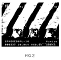
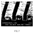
- FIG. 2 A Scanning Electron Micrograph (SEM), of one of the wafers after processing is shown in Figure 2. All the SEM's shown in Figs 2-7 of this example were done at 10 KEV using various magnifications and resolutions. Views from the top as well as the sides are also shown. Specifically, Figure 2 shows the metal line structure of the RIE wafer which contains RIE residue deposit thereon.
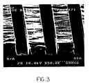
- a first experiment one of the wafers was exposed to supercritical fluid CO 2 for 2 hrs at a temperature of 40°C and a pressure of 5840 psi.
- An SEM for this experiment is shown in Fig. 3. Specifically, this SEM shows a cleaned semiconductor sample. The sample initially contained RIE residue prior to exposure to a supercritical fluid under the above conditions.
- Fig. 8 side view
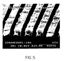
- the wafer was exposed to supercritical fluid CO 2 for 1 hour at 3000 psi and 40°C with stirring at 500 rpm.
- Figure Fig. 9 side view
- all RIE residue has been removed from the sample under these conditions.
Abstract
Description
In an article by Ziger et al. entitled "Compressed Fluid Technology: Application to RIE-Developed Resists", AICHE Journal, Vol. 33, No. 10, October 1978, compressed CO2 i.e., supercritical fluid CO2, is utilized in the area of microlithography to extract nonvolatile siloxane molecules from a host organic polymer.
Claims (25)
- A method for removing residue from an etched precision surface comprising exposing said precision surface to a removing fluid comprising supercritical fluid or liquid CO2 under conditions sufficient to remove said residue from said etch precision surface.
- The method of claim 1 wherein said removing fluid is a supercritical fluid.
- The method of Claim 2 wherein said supercritical fluid comprises Ar or CO2 or mixtures thereof.
- The method of Claim 2 wherein said surface is exposed to said supercritical fluid at a pressure of from about 1000 psi to about 6000 psi.
- The method of Claim 4 wherein said pressure is about 3000 psi.
- The method of Claim 2 wherein said surface is exposed to said supercritical fluid at a temperature of about 40°C to about 80°C.
- The method of claim 1 wherein said removing fluid is liquid CO2.
- The method of Claim 1, 2 or 7 wherein the precision surface is a semiconductor sample, a metal, a polymer or an insulator.
- The method of Claims 1 to 8 wherein the precision surface is etched by reactive ion etching, ion beam etching, plasma etching or laser ablation.
- The method of Claim 9 wherein etching is conducted by reactive ion etching.
- The method of Claim 7 wherein said precision surface is exposed to said liquid CO2 at a pressure of about 880 psi to about 1000 psi.
- The method of Claim 7 wherein said precision surface is exposed to said liquid CO2 at a temperature of from about 25°C to about 40°C.
- The method of Claim 1, 2 or 7 wherein said precision surface is exposed to said removing liquid for a time period of about 30 minutes to about 2 hrs.
- The method of Claim 13 wherein said exposure time is about 1 hr.
- The method of Claim 8 wherein said semiconductor sample is a surface of a semiconductor wafer, semiconductor chip, ceramic substrate, glass substrate, polymer or other patterned film structure.
- The method of claim 1, 2 or 7 wherein said precision surface contains a material selected from the group consisting of titanium silicide, tantalum nitride, silicon, polysilicon, silicon nitride, SiO2, diamond- like carbon, polyimides, polyamides, aluminum, aluminum with copper, copper, Ti, Ta, W, Pt, Pd, Ir, Cr, ferroelectric materials and high dielectric materials.
- The method of Claim 1, 2 or 7 wherein said removing fluid is stirred at about 500 rpm to about 2500 rpm.
- The method of Claim 17 wherein said removing fluid is stirred at about 1000 rpm.
- The method of Claim 1, 2 or 7 wherein an additive or surfactant is used with said removing fluid.
- The method of Claim 19 wherein said additive is selected from the group consisting of Ar, N2O, NH3, N2, CH4, C2H4, CHF3, C2H6, n-C3H8 and H2O.
- The method of Claim 19 wherein said surfactant is a surfactant which contains at least one CFx functional groups.
- The method of Claim 1, 2 or 7 wherein said removing fluid is purified prior to exposing to said precision surface.
- The method of Claim 1, 2 or 7 wherein said residue contains at least one element selected from the group consisting of carbon, hydrogen, silicon, aluminum, W, Ti, Ta, Pt, Pd, Ir, Cr, fluorine and chlorine.
- The method of Claim 1, 2 or 7 further comprising contacting said removing fluid exposed precision surface with a cryogenic aerosol under conditions sufficient to remove any remaining residue from the exposed precision surface.
- The method of Claim 24 wherein said cryogenic aerosol of Ar, N2, CO2 or a mixture thereof.
Applications Claiming Priority (2)
| Application Number | Priority Date | Filing Date | Title |
|---|---|---|---|
| US731538 | 1996-10-16 | ||
| US08/731,538 US5908510A (en) | 1996-10-16 | 1996-10-16 | Residue removal by supercritical fluids |
Publications (2)
| Publication Number | Publication Date |
|---|---|
| EP0836895A2 true EP0836895A2 (en) | 1998-04-22 |
| EP0836895A3 EP0836895A3 (en) | 1998-09-16 |
Family
ID=24939946
Family Applications (1)
| Application Number | Title | Priority Date | Filing Date |
|---|---|---|---|
| EP97307272A Withdrawn EP0836895A3 (en) | 1996-10-16 | 1997-09-18 | Residue removal by supercritical fluids |
Country Status (4)
| Country | Link |
|---|---|
| US (2) | US5908510A (en) |
| EP (1) | EP0836895A3 (en) |
| JP (1) | JP3358172B2 (en) |
| KR (1) | KR100330616B1 (en) |
Cited By (20)
| Publication number | Priority date | Publication date | Assignee | Title |
|---|---|---|---|---|
| WO2000039847A1 (en) * | 1998-12-23 | 2000-07-06 | Infineon Technologies Ag | Method for structuring a substrate and device for carrying out said method |
| WO2001017699A1 (en) * | 1999-09-04 | 2001-03-15 | Messer Griesheim Gmbh | Method for cleaning substrate surfaces |
| WO2001033613A2 (en) * | 1999-11-02 | 2001-05-10 | Tokyo Electron Limited | Removal of photoresist and residue from substrate using supercritical carbon dioxide process |
| WO2002015251A1 (en) * | 2000-08-14 | 2002-02-21 | Tokyo Electron Limited | Removal of photoresist and photoresist residue from semiconductors using supercritical carbon dioxide process |
| EP1214555A1 (en) * | 1999-09-20 | 2002-06-19 | S. C. Fluids, Inc. | Supercritical fluid drying system |
| US6457480B1 (en) * | 2001-06-27 | 2002-10-01 | International Business Machines Corporation | Process and apparatus for cleaning filters |
| US6509141B2 (en) | 1997-05-27 | 2003-01-21 | Tokyo Electron Limited | Removal of photoresist and photoresist residue from semiconductors using supercritical carbon dioxide process |
| WO2003024630A1 (en) * | 2001-09-14 | 2003-03-27 | Micell Technologies, Inc. | Method and apparatus for cleaning substrates using liquid carbon dioxide |
| EP1388376A2 (en) * | 2002-08-09 | 2004-02-11 | MESSER GRIESHEIM GmbH | Cleaning using CO2 and N2O |
| DE10236485A1 (en) * | 2002-08-09 | 2004-02-19 | Messer Griesheim Gmbh | Alternative dry cleaning medium with diverse applications, contains carbon dioxide and nitrous oxide in fifty-fifty proportions |
| DE10236491A1 (en) * | 2002-08-09 | 2004-02-19 | Messer Griesheim Gmbh | Alternative dry cleaning medium with diverse applications, contains carbon dioxide and nitrous oxide in fifty-fifty proportions |
| DE10236493A1 (en) * | 2002-08-09 | 2004-02-19 | Messer Griesheim Gmbh | Alternative dry cleaning medium with diverse applications, contains carbon dioxide and nitrous oxide in fifty-fifty proportions |
| US6736149B2 (en) | 1999-11-02 | 2004-05-18 | Supercritical Systems, Inc. | Method and apparatus for supercritical processing of multiple workpieces |
| EP1441836A1 (en) * | 2001-10-17 | 2004-08-04 | Praxair Technology, Inc. | Central carbon dioxide purifier |
| US6782900B2 (en) | 2001-09-13 | 2004-08-31 | Micell Technologies, Inc. | Methods and apparatus for cleaning and/or treating a substrate using CO2 |
| US7017637B2 (en) | 2001-09-25 | 2006-03-28 | Dainippon Screen Mfg. Co. Ltd. | Thin film forming apparatus and thin film forming method |
| US7195676B2 (en) | 2004-07-13 | 2007-03-27 | Air Products And Chemicals, Inc. | Method for removal of flux and other residue in dense fluid systems |
| US7211553B2 (en) | 2003-08-05 | 2007-05-01 | Air Products And Chemicals, Inc. | Processing of substrates with dense fluids comprising acetylenic diols and/or alcohols |
| US7267727B2 (en) | 2002-09-24 | 2007-09-11 | Air Products And Chemicals, Inc. | Processing of semiconductor components with dense processing fluids and ultrasonic energy |
| US7789971B2 (en) | 2005-05-13 | 2010-09-07 | Tokyo Electron Limited | Treatment of substrate using functionalizing agent in supercritical carbon dioxide |
Families Citing this family (125)
| Publication number | Priority date | Publication date | Assignee | Title |
|---|---|---|---|---|
| KR100417647B1 (en) * | 1996-12-28 | 2004-04-13 | 주식회사 하이닉스반도체 | Method for cleaning semiconductor device |
| WO1999049998A1 (en) * | 1998-03-30 | 1999-10-07 | The Regents Of The University Of California | Composition and method for removing photoresist materials from electronic components |
| US6846789B2 (en) | 1998-03-30 | 2005-01-25 | The Regents Of The University Of California | Composition and method for removing photoresist materials from electronic components |
| KR20000003955A (en) * | 1998-06-30 | 2000-01-25 | 김영환 | Cleaning method of semiconductor device using supercritical fluid |
| US6057230A (en) * | 1998-09-17 | 2000-05-02 | Taiwan Semiconductor Manufacturing Company, Ltd. | Dry etching procedure and recipe for patterning of thin film copper layers |
| US6277753B1 (en) | 1998-09-28 | 2001-08-21 | Supercritical Systems Inc. | Removal of CMP residue from semiconductors using supercritical carbon dioxide process |
| EP1024524A2 (en) | 1999-01-27 | 2000-08-02 | Matsushita Electric Industrial Co., Ltd. | Deposition of dielectric layers using supercritical CO2 |
| US7044143B2 (en) * | 1999-05-14 | 2006-05-16 | Micell Technologies, Inc. | Detergent injection systems and methods for carbon dioxide microelectronic substrate processing systems |
| US6235453B1 (en) * | 1999-07-07 | 2001-05-22 | Advanced Micro Devices, Inc. | Low-k photoresist removal process |
| US6602349B2 (en) | 1999-08-05 | 2003-08-05 | S.C. Fluids, Inc. | Supercritical fluid cleaning process for precision surfaces |
| US6612317B2 (en) | 2000-04-18 | 2003-09-02 | S.C. Fluids, Inc | Supercritical fluid delivery and recovery system for semiconductor wafer processing |
| US6383329B1 (en) | 1999-08-10 | 2002-05-07 | Xerox Corporation | Apparatus and method for removing a label from a surface with a chilled medium |
| US6734121B2 (en) * | 1999-09-02 | 2004-05-11 | Micron Technology, Inc. | Methods of treating surfaces of substrates |
| US6397421B1 (en) * | 1999-09-24 | 2002-06-04 | Micell Technologies | Methods and apparatus for conserving vapor and collecting liquid carbon dioxide for carbon dioxide dry cleaning |
| US6314601B1 (en) * | 1999-09-24 | 2001-11-13 | Mcclain James B. | System for the control of a carbon dioxide cleaning apparatus |
| US6558475B1 (en) | 2000-04-10 | 2003-05-06 | International Business Machines Corporation | Process for cleaning a workpiece using supercritical carbon dioxide |
| AU2001253650A1 (en) * | 2000-04-18 | 2001-10-30 | S. C. Fluids, Inc. | Supercritical fluid delivery and recovery system for semiconductor wafer processing |
| US20040025908A1 (en) * | 2000-04-18 | 2004-02-12 | Stephen Douglas | Supercritical fluid delivery system for semiconductor wafer processing |
| IL152376A0 (en) * | 2000-04-25 | 2003-05-29 | Tokyo Electron Ltd | Method of depositing metal film and metal deposition cluster tool including supercritical drying/cleaning module |
| WO2002009147A2 (en) * | 2000-07-26 | 2002-01-31 | Tokyo Electron Limited | High pressure processing chamber for semiconductor substrate |
| US6627002B1 (en) | 2000-07-28 | 2003-09-30 | Xerox Corporation | Hollow cylindrical imaging member treatment process with solid carbon dioxide pellets |
| US6416389B1 (en) | 2000-07-28 | 2002-07-09 | Xerox Corporation | Process for roughening a surface |
| US20040011378A1 (en) * | 2001-08-23 | 2004-01-22 | Jackson David P | Surface cleaning and modification processes, methods and apparatus using physicochemically modified dense fluid sprays |
| US6346484B1 (en) | 2000-08-31 | 2002-02-12 | International Business Machines Corporation | Method for selective extraction of sacrificial place-holding material used in fabrication of air gap-containing interconnect structures |
| KR100385432B1 (en) * | 2000-09-19 | 2003-05-27 | 주식회사 케이씨텍 | Surface cleaning aerosol production system |
| US6851319B2 (en) * | 2000-09-27 | 2005-02-08 | Digital Wave Corporation | Device and method designed for ultrasonically inspecting cylinders for longitudinal and circumferential defects and to measure wall thickness |
| US6623355B2 (en) * | 2000-11-07 | 2003-09-23 | Micell Technologies, Inc. | Methods, apparatus and slurries for chemical mechanical planarization |
| KR20020052488A (en) * | 2000-12-26 | 2002-07-04 | 박종섭 | A method for manufacturing a fine pattern of a semiconductor device |
| US6425956B1 (en) | 2001-01-05 | 2002-07-30 | International Business Machines Corporation | Process for removing chemical mechanical polishing residual slurry |
| US6451375B1 (en) | 2001-01-05 | 2002-09-17 | International Business Machines Corporation | Process for depositing a film on a nanometer structure |
| JP2002237481A (en) * | 2001-02-09 | 2002-08-23 | Kobe Steel Ltd | Method of cleaning microscopic structure |
| US6613157B2 (en) | 2001-02-15 | 2003-09-02 | Micell Technologies, Inc. | Methods for removing particles from microelectronic structures |
| US6596093B2 (en) | 2001-02-15 | 2003-07-22 | Micell Technologies, Inc. | Methods for cleaning microelectronic structures with cyclical phase modulation |
| US6641678B2 (en) | 2001-02-15 | 2003-11-04 | Micell Technologies, Inc. | Methods for cleaning microelectronic structures with aqueous carbon dioxide systems |
| US6602351B2 (en) | 2001-02-15 | 2003-08-05 | Micell Technologies, Inc. | Methods for the control of contaminants following carbon dioxide cleaning of microelectronic structures |
| US6905555B2 (en) | 2001-02-15 | 2005-06-14 | Micell Technologies, Inc. | Methods for transferring supercritical fluids in microelectronic and other industrial processes |
| US6562146B1 (en) * | 2001-02-15 | 2003-05-13 | Micell Technologies, Inc. | Processes for cleaning and drying microelectronic structures using liquid or supercritical carbon dioxide |
| IL158340A0 (en) * | 2001-04-10 | 2004-05-12 | Supercritical Systems Inc | High pressure processing chamber for semiconductor substrate including flow enhancing features |
| US6823880B2 (en) * | 2001-04-25 | 2004-11-30 | Kabushiki Kaisha Kobe Seiko Sho | High pressure processing apparatus and high pressure processing method |
| US6890855B2 (en) | 2001-06-27 | 2005-05-10 | International Business Machines Corporation | Process of removing residue material from a precision surface |
| US6509136B1 (en) | 2001-06-27 | 2003-01-21 | International Business Machines Corporation | Process of drying a cast polymeric film disposed on a workpiece |
| US6454869B1 (en) * | 2001-06-27 | 2002-09-24 | International Business Machines Corporation | Process of cleaning semiconductor processing, handling and manufacturing equipment |
| US6398875B1 (en) | 2001-06-27 | 2002-06-04 | International Business Machines Corporation | Process of drying semiconductor wafers using liquid or supercritical carbon dioxide |
| US6653233B2 (en) | 2001-06-27 | 2003-11-25 | International Business Machines Corporation | Process of providing a semiconductor device with electrical interconnection capability |
| US20030008129A1 (en) | 2001-06-27 | 2003-01-09 | International Business Machines Corporation | Dielectric material and process of insulating a semiconductor device using same |
| US6946055B2 (en) * | 2001-08-22 | 2005-09-20 | International Business Machines Corporation | Method for recovering an organic solvent from a waste stream containing supercritical CO2 |
| US6838015B2 (en) | 2001-09-04 | 2005-01-04 | International Business Machines Corporation | Liquid or supercritical carbon dioxide composition |
| US6619304B2 (en) | 2001-09-13 | 2003-09-16 | Micell Technologies, Inc. | Pressure chamber assembly including non-mechanical drive means |
| US6706641B2 (en) | 2001-09-13 | 2004-03-16 | Micell Technologies, Inc. | Spray member and method for using the same |
| US6666928B2 (en) | 2001-09-13 | 2003-12-23 | Micell Technologies, Inc. | Methods and apparatus for holding a substrate in a pressure chamber |
| US20040040660A1 (en) * | 2001-10-03 | 2004-03-04 | Biberger Maximilian Albert | High pressure processing chamber for multiple semiconductor substrates |
| US6848458B1 (en) * | 2002-02-05 | 2005-02-01 | Novellus Systems, Inc. | Apparatus and methods for processing semiconductor substrates using supercritical fluids |
| US20080264443A1 (en) * | 2002-02-05 | 2008-10-30 | Novellus Systems, Inc. | Apparatus and methods for increasing the rate of solute concentration evolution in a supercritical process chamber |
| US6766810B1 (en) * | 2002-02-15 | 2004-07-27 | Novellus Systems, Inc. | Methods and apparatus to control pressure in a supercritical fluid reactor |
| KR20030068772A (en) * | 2002-02-18 | 2003-08-25 | 태화일렉트론(주) | Cleaning equipment for LCD panel |
| US6953654B2 (en) | 2002-03-14 | 2005-10-11 | Tokyo Electron Limited | Process and apparatus for removing a contaminant from a substrate |
| US20040003828A1 (en) * | 2002-03-21 | 2004-01-08 | Jackson David P. | Precision surface treatments using dense fluids and a plasma |
| JP2005522056A (en) * | 2002-04-05 | 2005-07-21 | ビーオーシー・インコーポレーテッド | Fluid assisted cryogenic cleaning |
| US6949145B2 (en) * | 2002-04-05 | 2005-09-27 | Boc, Inc. | Vapor-assisted cryogenic cleaning |
| US6852173B2 (en) * | 2002-04-05 | 2005-02-08 | Boc, Inc. | Liquid-assisted cryogenic cleaning |
| US20050217706A1 (en) * | 2002-04-05 | 2005-10-06 | Souvik Banerjee | Fluid assisted cryogenic cleaning |
| US6764552B1 (en) | 2002-04-18 | 2004-07-20 | Novellus Systems, Inc. | Supercritical solutions for cleaning photoresist and post-etch residue from low-k materials |
| US20040045578A1 (en) * | 2002-05-03 | 2004-03-11 | Jackson David P. | Method and apparatus for selective treatment of a precision substrate surface |
| US6669785B2 (en) | 2002-05-15 | 2003-12-30 | Micell Technologies, Inc. | Methods and compositions for etch cleaning microelectronic substrates in carbon dioxide |
| US20030217764A1 (en) * | 2002-05-23 | 2003-11-27 | Kaoru Masuda | Process and composition for removing residues from the microstructure of an object |
| US6846380B2 (en) * | 2002-06-13 | 2005-01-25 | The Boc Group, Inc. | Substrate processing apparatus and related systems and methods |
| US20040011386A1 (en) * | 2002-07-17 | 2004-01-22 | Scp Global Technologies Inc. | Composition and method for removing photoresist and/or resist residue using supercritical fluids |
| US20040050406A1 (en) * | 2002-07-17 | 2004-03-18 | Akshey Sehgal | Compositions and method for removing photoresist and/or resist residue at pressures ranging from ambient to supercritical |
| US6764873B2 (en) * | 2002-07-18 | 2004-07-20 | International Business Machines Corporation | Semiconductor wafer including a low dielectric constant thermosetting polymer film and method of making same |
| US6764385B2 (en) * | 2002-07-29 | 2004-07-20 | Nanoclean Technologies, Inc. | Methods for resist stripping and cleaning surfaces substantially free of contaminants |
| US7297286B2 (en) * | 2002-07-29 | 2007-11-20 | Nanoclean Technologies, Inc. | Methods for resist stripping and other processes for cleaning surfaces substantially free of contaminants |
| US7101260B2 (en) * | 2002-07-29 | 2006-09-05 | Nanoclean Technologies, Inc. | Methods for resist stripping and other processes for cleaning surfaces substantially free of contaminants |
| US7134941B2 (en) * | 2002-07-29 | 2006-11-14 | Nanoclean Technologies, Inc. | Methods for residue removal and corrosion prevention in a post-metal etch process |
| US7066789B2 (en) * | 2002-07-29 | 2006-06-27 | Manoclean Technologies, Inc. | Methods for resist stripping and other processes for cleaning surfaces substantially free of contaminants |
| US20080004194A1 (en) * | 2002-09-24 | 2008-01-03 | Air Products And Chemicals, Inc. | Processing of semiconductor components with dense processing fluids |
| US20080000505A1 (en) * | 2002-09-24 | 2008-01-03 | Air Products And Chemicals, Inc. | Processing of semiconductor components with dense processing fluids |
| US7282099B2 (en) * | 2002-09-24 | 2007-10-16 | Air Products And Chemicals, Inc. | Dense phase processing fluids for microelectronic component manufacture |
| US6953041B2 (en) * | 2002-10-09 | 2005-10-11 | Micell Technologies, Inc. | Compositions of transition metal species in dense phase carbon dioxide and methods of use thereof |
| US6943139B2 (en) * | 2002-10-31 | 2005-09-13 | Advanced Technology Materials, Inc. | Removal of particle contamination on patterned silicon/silicon dioxide using supercritical carbon dioxide/chemical formulations |
| US20060019850A1 (en) * | 2002-10-31 | 2006-01-26 | Korzenski Michael B | Removal of particle contamination on a patterned silicon/silicon dioxide using dense fluid/chemical formulations |
| JP2004158534A (en) * | 2002-11-05 | 2004-06-03 | Kobe Steel Ltd | Method for cleaning microscopic structure |
| US6880560B2 (en) * | 2002-11-18 | 2005-04-19 | Techsonic | Substrate processing apparatus for processing substrates using dense phase gas and sonic waves |
| US6683008B1 (en) | 2002-11-19 | 2004-01-27 | International Business Machines Corporation | Process of removing ion-implanted photoresist from a workpiece |
| US20040112409A1 (en) * | 2002-12-16 | 2004-06-17 | Supercritical Sysems, Inc. | Fluoride in supercritical fluid for photoresist and residue removal |
| US6875286B2 (en) * | 2002-12-16 | 2005-04-05 | International Business Machines Corporation | Solid CO2 cleaning |
| US20040154647A1 (en) * | 2003-02-07 | 2004-08-12 | Supercritical Systems, Inc. | Method and apparatus of utilizing a coating for enhanced holding of a semiconductor substrate during high pressure processing |
| US20040198066A1 (en) * | 2003-03-21 | 2004-10-07 | Applied Materials, Inc. | Using supercritical fluids and/or dense fluids in semiconductor applications |
| US20040194886A1 (en) * | 2003-04-01 | 2004-10-07 | Deyoung James | Microelectronic device manufacturing in coordinated carbon dioxide processing chambers |
| US6875285B2 (en) * | 2003-04-24 | 2005-04-05 | Taiwan Semiconductor Manufacturing Company, Ltd. | System and method for dampening high pressure impact on porous materials |
| KR100505693B1 (en) * | 2003-06-26 | 2005-08-03 | 삼성전자주식회사 | Cleaning method of photoresist or organic material from microelectronic device substrate |
| US20050006310A1 (en) * | 2003-07-10 | 2005-01-13 | Rajat Agrawal | Purification and recovery of fluids in processing applications |
| US7323064B2 (en) * | 2003-08-06 | 2008-01-29 | Micron Technology, Inc. | Supercritical fluid technology for cleaning processing chambers and systems |
| US20050087490A1 (en) * | 2003-10-28 | 2005-04-28 | International Business Machines Corporation | Process for removing impurities from low dielectric constant films disposed on semiconductor devices |
| US7069742B2 (en) * | 2004-01-19 | 2006-07-04 | Air Products And Chemicals, Inc. | High-pressure delivery system for ultra high purity liquid carbon dioxide |
| US7076969B2 (en) * | 2004-01-19 | 2006-07-18 | Air Products And Chemicals, Inc. | System for supply and delivery of high purity and ultrahigh purity carbon dioxide |
| US7076970B2 (en) * | 2004-01-19 | 2006-07-18 | Air Products And Chemicals, Inc. | System for supply and delivery of carbon dioxide with different purity requirements |
| US7264679B2 (en) * | 2004-02-11 | 2007-09-04 | Applied Materials, Inc. | Cleaning of chamber components |
| US20050183740A1 (en) * | 2004-02-19 | 2005-08-25 | Fulton John L. | Process and apparatus for removing residues from semiconductor substrates |
| CA2467316A1 (en) * | 2004-05-14 | 2005-11-14 | British Columbia Hydro And Power Authority | Dry ice blasting cleaning apparatus |
| US20050279453A1 (en) * | 2004-06-17 | 2005-12-22 | Uvtech Systems, Inc. | System and methods for surface cleaning |
| CN100528292C (en) * | 2004-10-07 | 2009-08-19 | 日本派欧尼株式会社 | Processing method of exhaust gas and processing apparatus of exhaust gas |
| US20060081273A1 (en) * | 2004-10-20 | 2006-04-20 | Mcdermott Wayne T | Dense fluid compositions and processes using same for article treatment and residue removal |
| WO2006076005A1 (en) * | 2005-01-12 | 2006-07-20 | Boc, Inc. | System for cleaning a surface using cryogenic aerosol and fluid reactant |
| US7008853B1 (en) * | 2005-02-25 | 2006-03-07 | Infineon Technologies, Ag | Method and system for fabricating free-standing nanostructures |
| JP4518986B2 (en) * | 2005-03-17 | 2010-08-04 | 東京エレクトロン株式会社 | Atmospheric transfer chamber, post-processing transfer method, program, and storage medium |
| US7407554B2 (en) * | 2005-04-12 | 2008-08-05 | International Business Machines Corporation | Development or removal of block copolymer or PMMA-b-S-based resist using polar supercritical solvent |
| WO2006138727A2 (en) * | 2005-06-17 | 2006-12-28 | The Regents Of The University Of Michigan | Apparatus and method of producing net-shape components from alloy sheets |
| JP4533809B2 (en) * | 2005-06-28 | 2010-09-01 | 株式会社東芝 | Method for manufacturing substrate for discrete track medium and method for manufacturing discrete track medium |
| US7588995B2 (en) * | 2005-11-14 | 2009-09-15 | Taiwan Semiconductor Manufacturing Company, Ltd. | Method to create damage-free porous low-k dielectric films and structures resulting therefrom |
| US7951723B2 (en) * | 2006-10-24 | 2011-05-31 | Taiwan Semiconductor Manufacturing Company, Ltd. | Integrated etch and supercritical CO2 process and chamber design |
| KR100885496B1 (en) * | 2007-07-11 | 2009-02-24 | 세메스 주식회사 | Supercritical fluid generating apparatus, and facility and method for treating substrate with the same |
| US7981221B2 (en) | 2008-02-21 | 2011-07-19 | Micron Technology, Inc. | Rheological fluids for particle removal |
| TWI352615B (en) * | 2009-06-09 | 2011-11-21 | Univ Nat Taiwan Science Tech | Fluid separation method and fluid seperation appar |
| KR101789841B1 (en) * | 2009-12-11 | 2017-10-25 | 램 리써치 코포레이션 | Method and system for handling a substrate through processes including an integrated electroless deposition process |
| JP5647845B2 (en) * | 2010-09-29 | 2015-01-07 | 株式会社Screenホールディングス | Substrate drying apparatus and substrate drying method |
| KR101485275B1 (en) * | 2011-02-18 | 2015-01-21 | 오르가노 코포레이션 | Method for cleaning filter, and method for washing or drying body to be treated |
| US9099547B2 (en) | 2011-10-04 | 2015-08-04 | Infineon Technologies Ag | Testing process for semiconductor devices |
| US8883565B2 (en) | 2011-10-04 | 2014-11-11 | Infineon Technologies Ag | Separation of semiconductor devices from a wafer carrier |
| KR102101343B1 (en) * | 2013-12-05 | 2020-04-17 | 삼성전자주식회사 | method for purifying supercritical fluid and purification apparatus of the same |
| WO2019055508A1 (en) * | 2017-09-12 | 2019-03-21 | Applied Materials, Inc. | Selective deposition defects removal by chemical etch |
| JP2019062039A (en) * | 2017-09-26 | 2019-04-18 | 株式会社東芝 | Etching apparatus and method, processing system, and article, semiconductor device, and manufacturing method for semiconductor chip |
| US11033930B2 (en) | 2018-01-08 | 2021-06-15 | Applied Materials, Inc. | Methods and apparatus for cryogenic gas stream assisted SAM-based selective deposition |
| TWI776026B (en) * | 2018-06-04 | 2022-09-01 | 美商帕斯馬舍門有限責任公司 | Method for dicing die attach film |
| KR102179716B1 (en) * | 2019-04-24 | 2020-11-17 | 무진전자 주식회사 | Substrate drying chamber |
| CN114078692B (en) * | 2022-01-07 | 2024-02-20 | 浙江大学杭州国际科创中心 | Wafer cleaning method and wafer cleaning equipment |
Citations (5)
| Publication number | Priority date | Publication date | Assignee | Title |
|---|---|---|---|---|
| EP0391035A2 (en) * | 1989-04-03 | 1990-10-10 | Hughes Aircraft Company | Dense fluid photochemical process for substrate treatment |
| US5267455A (en) * | 1992-07-13 | 1993-12-07 | The Clorox Company | Liquid/supercritical carbon dioxide dry cleaning system |
| EP0587168A1 (en) * | 1992-09-11 | 1994-03-16 | Linde Aktiengesellschaft | Cleaning installation with liquid or supercritical gases |
| US5377705A (en) * | 1993-09-16 | 1995-01-03 | Autoclave Engineers, Inc. | Precision cleaning system |
| US5522938A (en) * | 1994-08-08 | 1996-06-04 | Texas Instruments Incorporated | Particle removal in supercritical liquids using single frequency acoustic waves |
Family Cites Families (20)
| Publication number | Priority date | Publication date | Assignee | Title |
|---|---|---|---|---|
| US3890176A (en) * | 1972-08-18 | 1975-06-17 | Gen Electric | Method for removing photoresist from substrate |
| US5105556A (en) * | 1987-08-12 | 1992-04-21 | Hitachi, Ltd. | Vapor washing process and apparatus |
| JP2663483B2 (en) * | 1988-02-29 | 1997-10-15 | 勝 西川 | Method of forming resist pattern |
| JPH01242621A (en) * | 1988-03-23 | 1989-09-27 | Mitsubishi Gas Chem Co Inc | Preparation of purified polycarbonate resin |
| US5185296A (en) * | 1988-07-26 | 1993-02-09 | Matsushita Electric Industrial Co., Ltd. | Method for forming a dielectric thin film or its pattern of high accuracy on a substrate |
| US5013366A (en) * | 1988-12-07 | 1991-05-07 | Hughes Aircraft Company | Cleaning process using phase shifting of dense phase gases |
| US5213619A (en) * | 1989-11-30 | 1993-05-25 | Jackson David P | Processes for cleaning, sterilizing, and implanting materials using high energy dense fluids |
| US5279771A (en) * | 1990-11-05 | 1994-01-18 | Ekc Technology, Inc. | Stripping compositions comprising hydroxylamine and alkanolamine |
| US5306350A (en) * | 1990-12-21 | 1994-04-26 | Union Carbide Chemicals & Plastics Technology Corporation | Methods for cleaning apparatus using compressed fluids |
| US5185058A (en) * | 1991-01-29 | 1993-02-09 | Micron Technology, Inc. | Process for etching semiconductor devices |
| KR930019861A (en) * | 1991-12-12 | 1993-10-19 | 완다 케이. 덴슨-로우 | Coating method using dense gas |
| US5313965A (en) * | 1992-06-01 | 1994-05-24 | Hughes Aircraft Company | Continuous operation supercritical fluid treatment process and system |
| US5344493A (en) * | 1992-07-20 | 1994-09-06 | Jackson David P | Cleaning process using microwave energy and centrifugation in combination with dense fluids |
| US5368171A (en) * | 1992-07-20 | 1994-11-29 | Jackson; David P. | Dense fluid microwave centrifuge |
| US5294261A (en) * | 1992-11-02 | 1994-03-15 | Air Products And Chemicals, Inc. | Surface cleaning using an argon or nitrogen aerosol |
| US5380401A (en) * | 1993-01-14 | 1995-01-10 | Micron Technology, Inc. | Method to remove fluorine residues from bond pads |
| US5378312A (en) * | 1993-12-07 | 1995-01-03 | International Business Machines Corporation | Process for fabricating a semiconductor structure having sidewalls |
| US5417768A (en) * | 1993-12-14 | 1995-05-23 | Autoclave Engineers, Inc. | Method of cleaning workpiece with solvent and then with liquid carbon dioxide |
| KR0137841B1 (en) * | 1994-06-07 | 1998-04-27 | 문정환 | Method for removing a etching waste material |
| DE69610652T2 (en) * | 1995-01-26 | 2001-05-10 | Texas Instruments Inc | Process for removing surface contamination |
-
1996
- 1996-10-16 US US08/731,538 patent/US5908510A/en not_active Expired - Fee Related
-
1997
- 1997-09-12 KR KR1019970046980A patent/KR100330616B1/en not_active IP Right Cessation
- 1997-09-18 EP EP97307272A patent/EP0836895A3/en not_active Withdrawn
- 1997-10-13 JP JP27892397A patent/JP3358172B2/en not_active Expired - Fee Related
-
1998
- 1998-11-30 US US09/201,459 patent/US5976264A/en not_active Expired - Fee Related
Patent Citations (5)
| Publication number | Priority date | Publication date | Assignee | Title |
|---|---|---|---|---|
| EP0391035A2 (en) * | 1989-04-03 | 1990-10-10 | Hughes Aircraft Company | Dense fluid photochemical process for substrate treatment |
| US5267455A (en) * | 1992-07-13 | 1993-12-07 | The Clorox Company | Liquid/supercritical carbon dioxide dry cleaning system |
| EP0587168A1 (en) * | 1992-09-11 | 1994-03-16 | Linde Aktiengesellschaft | Cleaning installation with liquid or supercritical gases |
| US5377705A (en) * | 1993-09-16 | 1995-01-03 | Autoclave Engineers, Inc. | Precision cleaning system |
| US5522938A (en) * | 1994-08-08 | 1996-06-04 | Texas Instruments Incorporated | Particle removal in supercritical liquids using single frequency acoustic waves |
Cited By (30)
| Publication number | Priority date | Publication date | Assignee | Title |
|---|---|---|---|---|
| US6500605B1 (en) | 1997-05-27 | 2002-12-31 | Tokyo Electron Limited | Removal of photoresist and residue from substrate using supercritical carbon dioxide process |
| US6509141B2 (en) | 1997-05-27 | 2003-01-21 | Tokyo Electron Limited | Removal of photoresist and photoresist residue from semiconductors using supercritical carbon dioxide process |
| DE19860084B4 (en) * | 1998-12-23 | 2005-12-22 | Infineon Technologies Ag | Method for structuring a substrate |
| WO2000039847A1 (en) * | 1998-12-23 | 2000-07-06 | Infineon Technologies Ag | Method for structuring a substrate and device for carrying out said method |
| WO2001017699A1 (en) * | 1999-09-04 | 2001-03-15 | Messer Griesheim Gmbh | Method for cleaning substrate surfaces |
| EP1214555A4 (en) * | 1999-09-20 | 2004-04-07 | S C Fluids Inc | Supercritical fluid drying system |
| EP1214555A1 (en) * | 1999-09-20 | 2002-06-19 | S. C. Fluids, Inc. | Supercritical fluid drying system |
| WO2001033613A2 (en) * | 1999-11-02 | 2001-05-10 | Tokyo Electron Limited | Removal of photoresist and residue from substrate using supercritical carbon dioxide process |
| US6748960B1 (en) | 1999-11-02 | 2004-06-15 | Tokyo Electron Limited | Apparatus for supercritical processing of multiple workpieces |
| US6736149B2 (en) | 1999-11-02 | 2004-05-18 | Supercritical Systems, Inc. | Method and apparatus for supercritical processing of multiple workpieces |
| WO2001033613A3 (en) * | 1999-11-02 | 2002-01-10 | Tokyo Electron Ltd | Removal of photoresist and residue from substrate using supercritical carbon dioxide process |
| WO2002015251A1 (en) * | 2000-08-14 | 2002-02-21 | Tokyo Electron Limited | Removal of photoresist and photoresist residue from semiconductors using supercritical carbon dioxide process |
| US6457480B1 (en) * | 2001-06-27 | 2002-10-01 | International Business Machines Corporation | Process and apparatus for cleaning filters |
| US6782900B2 (en) | 2001-09-13 | 2004-08-31 | Micell Technologies, Inc. | Methods and apparatus for cleaning and/or treating a substrate using CO2 |
| WO2003024630A1 (en) * | 2001-09-14 | 2003-03-27 | Micell Technologies, Inc. | Method and apparatus for cleaning substrates using liquid carbon dioxide |
| US6763840B2 (en) | 2001-09-14 | 2004-07-20 | Micell Technologies, Inc. | Method and apparatus for cleaning substrates using liquid carbon dioxide |
| US7017637B2 (en) | 2001-09-25 | 2006-03-28 | Dainippon Screen Mfg. Co. Ltd. | Thin film forming apparatus and thin film forming method |
| EP1441836A4 (en) * | 2001-10-17 | 2006-04-19 | Praxair Technology Inc | Central carbon dioxide purifier |
| EP1441836A1 (en) * | 2001-10-17 | 2004-08-04 | Praxair Technology, Inc. | Central carbon dioxide purifier |
| DE10236491A1 (en) * | 2002-08-09 | 2004-02-19 | Messer Griesheim Gmbh | Alternative dry cleaning medium with diverse applications, contains carbon dioxide and nitrous oxide in fifty-fifty proportions |
| DE10236493A1 (en) * | 2002-08-09 | 2004-02-19 | Messer Griesheim Gmbh | Alternative dry cleaning medium with diverse applications, contains carbon dioxide and nitrous oxide in fifty-fifty proportions |
| DE10236485A1 (en) * | 2002-08-09 | 2004-02-19 | Messer Griesheim Gmbh | Alternative dry cleaning medium with diverse applications, contains carbon dioxide and nitrous oxide in fifty-fifty proportions |
| EP1388376A2 (en) * | 2002-08-09 | 2004-02-11 | MESSER GRIESHEIM GmbH | Cleaning using CO2 and N2O |
| EP1388376A3 (en) * | 2002-08-09 | 2007-01-10 | Air Liquide Deutschland GmbH | Cleaning using CO2 and N2O |
| DE10236491B4 (en) * | 2002-08-09 | 2012-05-03 | Air Liquide Deutschland Gmbh | Cleaning with CO2 and N2O |
| DE10236485B4 (en) * | 2002-08-09 | 2012-10-11 | Air Liquide Deutschland Gmbh | Cleaning substrate surfaces using CO2 and N2O |
| US7267727B2 (en) | 2002-09-24 | 2007-09-11 | Air Products And Chemicals, Inc. | Processing of semiconductor components with dense processing fluids and ultrasonic energy |
| US7211553B2 (en) | 2003-08-05 | 2007-05-01 | Air Products And Chemicals, Inc. | Processing of substrates with dense fluids comprising acetylenic diols and/or alcohols |
| US7195676B2 (en) | 2004-07-13 | 2007-03-27 | Air Products And Chemicals, Inc. | Method for removal of flux and other residue in dense fluid systems |
| US7789971B2 (en) | 2005-05-13 | 2010-09-07 | Tokyo Electron Limited | Treatment of substrate using functionalizing agent in supercritical carbon dioxide |
Also Published As
| Publication number | Publication date |
|---|---|
| JPH10125644A (en) | 1998-05-15 |
| KR100330616B1 (en) | 2002-06-20 |
| US5976264A (en) | 1999-11-02 |
| KR19980032377A (en) | 1998-07-25 |
| EP0836895A3 (en) | 1998-09-16 |
| JP3358172B2 (en) | 2002-12-16 |
| US5908510A (en) | 1999-06-01 |
Similar Documents
| Publication | Publication Date | Title |
|---|---|---|
| US5908510A (en) | Residue removal by supercritical fluids | |
| US6890855B2 (en) | Process of removing residue material from a precision surface | |
| US6509141B2 (en) | Removal of photoresist and photoresist residue from semiconductors using supercritical carbon dioxide process | |
| EP0390134B1 (en) | Method and apparatus for cleaning semiconductor devices | |
| US6352081B1 (en) | Method of cleaning a semiconductor device processing chamber after a copper etch process | |
| US5925577A (en) | Method for forming via contact hole in a semiconductor device | |
| US20020088477A1 (en) | Process for removing chemical mechanical polishing residual slurry | |
| CA1235630A (en) | Etching techniques | |
| CA1136525A (en) | Dry etching of metal film | |
| US4505782A (en) | Plasma reactive ion etching of aluminum and aluminum alloys | |
| US20030027085A1 (en) | Removal of photoresist and photoresist residue from semiconductors using supercritical carbon dioxide process | |
| US6838015B2 (en) | Liquid or supercritical carbon dioxide composition | |
| KR20010033061A (en) | Method for high temperature etching of patterned layers using an organic mask stack | |
| US5749975A (en) | Process for dry cleaning wafer surfaces using a surface diffusion layer | |
| US5851302A (en) | Method for dry etching sidewall polymer | |
| US5792275A (en) | Film removal by chemical transformation and aerosol clean | |
| US4203800A (en) | Reactive ion etching process for metals | |
| US6758223B1 (en) | Plasma RIE polymer removal | |
| JP2004200658A (en) | Solid co2 purification | |
| JP2001508944A (en) | Metallization layer passivation method | |
| KR100568381B1 (en) | Cleaning fluid and cleaning method for component of semiconductor-treating apparatus | |
| WO2000039847A1 (en) | Method for structuring a substrate and device for carrying out said method | |
| US5755891A (en) | Method for post-etching of metal patterns | |
| Korzenski et al. | Supercritical carbon dioxide: the next generation solvent for semiconductor wafer cleaning technology | |
| EP1321977A1 (en) | Method for reducing residual electric charge created by a previous process step on a conductive structure |
Legal Events
| Date | Code | Title | Description |
|---|---|---|---|
| PUAI | Public reference made under article 153(3) epc to a published international application that has entered the european phase |
Free format text: ORIGINAL CODE: 0009012 |
|
| AK | Designated contracting states |
Kind code of ref document: A2 Designated state(s): AT BE CH DE DK ES FI FR GB GR IE IT LI LU MC NL PT SE |
|
| AX | Request for extension of the european patent |
Free format text: AL;LT;LV;RO;SI |
|
| PUAL | Search report despatched |
Free format text: ORIGINAL CODE: 0009013 |
|
| AK | Designated contracting states |
Kind code of ref document: A3 Designated state(s): AT BE CH DE DK ES FI FR GB GR IE IT LI LU MC NL PT SE |
|
| AX | Request for extension of the european patent |
Free format text: AL;LT;LV;RO;SI |
|
| AKX | Designation fees paid | ||
| RBV | Designated contracting states (corrected) | ||
| STAA | Information on the status of an ep patent application or granted ep patent |
Free format text: STATUS: THE APPLICATION IS DEEMED TO BE WITHDRAWN |
|
| 18D | Application deemed to be withdrawn |
Effective date: 19990317 |
|
| REG | Reference to a national code |
Ref country code: DE Ref legal event code: 8566 |