EP0825652A2 - Ohmic electrode and method of forming the same - Google Patents
Ohmic electrode and method of forming the same Download PDFInfo
- Publication number
- EP0825652A2 EP0825652A2 EP97111565A EP97111565A EP0825652A2 EP 0825652 A2 EP0825652 A2 EP 0825652A2 EP 97111565 A EP97111565 A EP 97111565A EP 97111565 A EP97111565 A EP 97111565A EP 0825652 A2 EP0825652 A2 EP 0825652A2
- Authority
- EP
- European Patent Office
- Prior art keywords
- layer
- compound semiconductor
- type compound
- transition metal
- platinum
- Prior art date
- Legal status (The legal status is an assumption and is not a legal conclusion. Google has not performed a legal analysis and makes no representation as to the accuracy of the status listed.)
- Granted
Links
- 238000000034 method Methods 0.000 title claims abstract description 35
- 239000004065 semiconductor Substances 0.000 claims abstract description 91
- 150000001875 compounds Chemical class 0.000 claims abstract description 82
- 229910052697 platinum Inorganic materials 0.000 claims abstract description 79
- 229910052737 gold Inorganic materials 0.000 claims abstract description 68
- 229910052723 transition metal Inorganic materials 0.000 claims abstract description 64
- 150000003624 transition metals Chemical class 0.000 claims abstract description 54
- 229910052757 nitrogen Inorganic materials 0.000 claims description 13
- 229910052733 gallium Inorganic materials 0.000 claims description 12
- 229910052782 aluminium Inorganic materials 0.000 claims description 10
- 229910052796 boron Inorganic materials 0.000 claims description 10
- 229910052738 indium Inorganic materials 0.000 claims description 10
- 238000001451 molecular beam epitaxy Methods 0.000 claims description 8
- 230000008569 process Effects 0.000 claims description 6
- 238000010438 heat treatment Methods 0.000 claims 2
- BASFCYQUMIYNBI-UHFFFAOYSA-N platinum Chemical compound [Pt] BASFCYQUMIYNBI-UHFFFAOYSA-N 0.000 abstract description 141
- 239000010931 gold Substances 0.000 abstract description 59
- PCHJSUWPFVWCPO-UHFFFAOYSA-N gold Chemical compound [Au] PCHJSUWPFVWCPO-UHFFFAOYSA-N 0.000 abstract description 58
- 238000000137 annealing Methods 0.000 abstract description 43
- 238000010030 laminating Methods 0.000 abstract description 3
- PXHVJJICTQNCMI-UHFFFAOYSA-N nickel Substances [Ni] PXHVJJICTQNCMI-UHFFFAOYSA-N 0.000 description 22
- KDLHZDBZIXYQEI-UHFFFAOYSA-N Palladium Chemical compound [Pd] KDLHZDBZIXYQEI-UHFFFAOYSA-N 0.000 description 19
- IJGRMHOSHXDMSA-UHFFFAOYSA-N Atomic nitrogen Chemical compound N#N IJGRMHOSHXDMSA-UHFFFAOYSA-N 0.000 description 18
- 229910052759 nickel Inorganic materials 0.000 description 11
- UFHFLCQGNIYNRP-UHFFFAOYSA-N Hydrogen Chemical compound [H][H] UFHFLCQGNIYNRP-UHFFFAOYSA-N 0.000 description 9
- 229910052763 palladium Inorganic materials 0.000 description 9
- 229910052751 metal Inorganic materials 0.000 description 8
- 239000002184 metal Substances 0.000 description 8
- 239000000758 substrate Substances 0.000 description 8
- GYHNNYVSQQEPJS-UHFFFAOYSA-N Gallium Chemical compound [Ga] GYHNNYVSQQEPJS-UHFFFAOYSA-N 0.000 description 7
- 230000004913 activation Effects 0.000 description 7
- 230000008859 change Effects 0.000 description 7
- 239000011777 magnesium Substances 0.000 description 6
- ZOXJGFHDIHLPTG-UHFFFAOYSA-N Boron Chemical compound [B] ZOXJGFHDIHLPTG-UHFFFAOYSA-N 0.000 description 5
- KRHYYFGTRYWZRS-UHFFFAOYSA-N Fluorane Chemical compound F KRHYYFGTRYWZRS-UHFFFAOYSA-N 0.000 description 5
- FYYHWMGAXLPEAU-UHFFFAOYSA-N Magnesium Chemical compound [Mg] FYYHWMGAXLPEAU-UHFFFAOYSA-N 0.000 description 5
- XAGFODPZIPBFFR-UHFFFAOYSA-N aluminium Chemical compound [Al] XAGFODPZIPBFFR-UHFFFAOYSA-N 0.000 description 5
- 230000004888 barrier function Effects 0.000 description 5
- 229910017052 cobalt Inorganic materials 0.000 description 5
- 239000010941 cobalt Substances 0.000 description 5
- GUTLYIVDDKVIGB-UHFFFAOYSA-N cobalt atom Chemical compound [Co] GUTLYIVDDKVIGB-UHFFFAOYSA-N 0.000 description 5
- 238000000151 deposition Methods 0.000 description 5
- 238000010586 diagram Methods 0.000 description 5
- 239000001257 hydrogen Substances 0.000 description 5
- 229910052739 hydrogen Inorganic materials 0.000 description 5
- APFVFJFRJDLVQX-UHFFFAOYSA-N indium atom Chemical compound [In] APFVFJFRJDLVQX-UHFFFAOYSA-N 0.000 description 5
- 229910052749 magnesium Inorganic materials 0.000 description 5
- 229910052594 sapphire Inorganic materials 0.000 description 5
- 239000010980 sapphire Substances 0.000 description 5
- 239000010936 titanium Substances 0.000 description 5
- RTAQQCXQSZGOHL-UHFFFAOYSA-N Titanium Chemical compound [Ti] RTAQQCXQSZGOHL-UHFFFAOYSA-N 0.000 description 4
- 229910052719 titanium Inorganic materials 0.000 description 4
- 239000012535 impurity Substances 0.000 description 3
- 150000004767 nitrides Chemical class 0.000 description 3
- DDFHBQSCUXNBSA-UHFFFAOYSA-N 5-(5-carboxythiophen-2-yl)thiophene-2-carboxylic acid Chemical compound S1C(C(=O)O)=CC=C1C1=CC=C(C(O)=O)S1 DDFHBQSCUXNBSA-UHFFFAOYSA-N 0.000 description 2
- ZOKXTWBITQBERF-UHFFFAOYSA-N Molybdenum Chemical compound [Mo] ZOKXTWBITQBERF-UHFFFAOYSA-N 0.000 description 2
- 238000004140 cleaning Methods 0.000 description 2
- 229910001873 dinitrogen Inorganic materials 0.000 description 2
- 230000000694 effects Effects 0.000 description 2
- 239000007788 liquid Substances 0.000 description 2
- 239000000463 material Substances 0.000 description 2
- 150000002739 metals Chemical class 0.000 description 2
- 239000000203 mixture Substances 0.000 description 2
- 229910052750 molybdenum Inorganic materials 0.000 description 2
- 239000011733 molybdenum Substances 0.000 description 2
- 229920002120 photoresistant polymer Polymers 0.000 description 2
- XLYOFNOQVPJJNP-UHFFFAOYSA-N water Substances O XLYOFNOQVPJJNP-UHFFFAOYSA-N 0.000 description 2
- 229910002704 AlGaN Inorganic materials 0.000 description 1
- 229910001218 Gallium arsenide Inorganic materials 0.000 description 1
- 239000000370 acceptor Substances 0.000 description 1
- 239000000956 alloy Substances 0.000 description 1
- 229910045601 alloy Inorganic materials 0.000 description 1
- 230000015572 biosynthetic process Effects 0.000 description 1
- 239000012159 carrier gas Substances 0.000 description 1
- 238000005229 chemical vapour deposition Methods 0.000 description 1
- 230000008021 deposition Effects 0.000 description 1
- 238000009792 diffusion process Methods 0.000 description 1
- 238000001035 drying Methods 0.000 description 1
- 238000010894 electron beam technology Methods 0.000 description 1
- 230000005669 field effect Effects 0.000 description 1
- 150000002431 hydrogen Chemical class 0.000 description 1
- 238000005259 measurement Methods 0.000 description 1
- QPJSUIGXIBEQAC-UHFFFAOYSA-N n-(2,4-dichloro-5-propan-2-yloxyphenyl)acetamide Chemical compound CC(C)OC1=CC(NC(C)=O)=C(Cl)C=C1Cl QPJSUIGXIBEQAC-UHFFFAOYSA-N 0.000 description 1
- 238000000206 photolithography Methods 0.000 description 1
- 230000005855 radiation Effects 0.000 description 1
- 230000000630 rising effect Effects 0.000 description 1
- 239000007787 solid Substances 0.000 description 1
- 239000000126 substance Substances 0.000 description 1
- 230000007704 transition Effects 0.000 description 1
Images


Classifications
-
- H—ELECTRICITY
- H01—ELECTRIC ELEMENTS
- H01L—SEMICONDUCTOR DEVICES NOT COVERED BY CLASS H10
- H01L21/00—Processes or apparatus adapted for the manufacture or treatment of semiconductor or solid state devices or of parts thereof
- H01L21/02—Manufacture or treatment of semiconductor devices or of parts thereof
- H01L21/04—Manufacture or treatment of semiconductor devices or of parts thereof the devices having at least one potential-jump barrier or surface barrier, e.g. PN junction, depletion layer or carrier concentration layer
- H01L21/18—Manufacture or treatment of semiconductor devices or of parts thereof the devices having at least one potential-jump barrier or surface barrier, e.g. PN junction, depletion layer or carrier concentration layer the devices having semiconductor bodies comprising elements of Group IV of the Periodic System or AIIIBV compounds with or without impurities, e.g. doping materials
- H01L21/28—Manufacture of electrodes on semiconductor bodies using processes or apparatus not provided for in groups H01L21/20 - H01L21/268
- H01L21/283—Deposition of conductive or insulating materials for electrodes conducting electric current
- H01L21/285—Deposition of conductive or insulating materials for electrodes conducting electric current from a gas or vapour, e.g. condensation
- H01L21/28506—Deposition of conductive or insulating materials for electrodes conducting electric current from a gas or vapour, e.g. condensation of conductive layers
- H01L21/28575—Deposition of conductive or insulating materials for electrodes conducting electric current from a gas or vapour, e.g. condensation of conductive layers on semiconductor bodies comprising AIIIBV compounds
-
- H—ELECTRICITY
- H01—ELECTRIC ELEMENTS
- H01L—SEMICONDUCTOR DEVICES NOT COVERED BY CLASS H10
- H01L29/00—Semiconductor devices adapted for rectifying, amplifying, oscillating or switching, or capacitors or resistors with at least one potential-jump barrier or surface barrier, e.g. PN junction depletion layer or carrier concentration layer; Details of semiconductor bodies or of electrodes thereof ; Multistep manufacturing processes therefor
- H01L29/40—Electrodes ; Multistep manufacturing processes therefor
- H01L29/43—Electrodes ; Multistep manufacturing processes therefor characterised by the materials of which they are formed
- H01L29/45—Ohmic electrodes
- H01L29/452—Ohmic electrodes on AIII-BV compounds
Definitions
- the present invention relates to an ohmic electrode for a p-type compound semiconductor layer containing at least one type among groups composed of gallium, aluminum, boron and indium as a III group element and nitrogen and a method of forming the ohmic electrode.
- Nitride III-V group semiconductors such as GaN, AlGaN, InGaN or BAlGaInN are considered to be promising as the material for forming a luminous element capable of emitting red or ultraviolet rays because of a reason that a band gap Eg can be varied from 1.8 eV to 6.2 eV. Further, attention is being paid also as a material for forming a Field Effect Transistor (FET) as an environment-proof element utilizing the property of a wide-gap semiconductor.
- FET Field Effect Transistor
- an ohmic electrode formed by laminating Ni and Au has been heretofore used as an ohmic electrode for a p-type GaN layer (Japanese Patent Laid-Open No. Hei 6-275868).
- the value of contact specific resistance is approximately 1x10 -2 ⁇ cm 2 , and has been fairly large as compared with the value of contact specific resistance in an ohmic electrode of another general semiconductor element (for example, approximately 1x10 -5 ⁇ cm 2 in an ohmic electrode for a p-type GaAs layer).
- the conventional ohmic electrode had such a specific character that the value of contact specific resistance becomes larger when annealing is performed at a temperature of 400°C or higher.
- the value of the contact specific resistance in the ohmic electrode for a p-type GaN layer is larger as compared with a value of contact specific resistance in an ohmic electrode of another general semiconductor element as described above because of such a reason that a large barrier against holes is produced on the interface between the semiconductor layer and the metal layer since an energy difference E V - ⁇ V (7.8 eV at RT) between the summit of a valence band and vacuum level of GaN is larger as compared with a work function ⁇ of a metal forming an electrode (for example, 5.2 eV for gold).
- the present invention has been made in view of such problems, and has for its object to provide an ohmic electrode in which the element can be made to operate stably for a long period by reducing the contact specific resistance and also increasing thermal stability thereof, and a method of forming the same.
- An ohmic electrode according to the present invention is used for a p-type compound semiconductor layer containing at least one type among groups composed of gallium, aluminum, boron and indium as a III group element and nitrogen, and is provided with an electrode layer composed of a complex containing at least one type among gold, platinum and a transition metal element other than gold or platinum.
- a method of forming an ohmic electrode according to the present invention is for forming an ohmic electrode for a p-type compound semiconductor layer containing at least one type among groups composed of gallium, aluminum, boron and indium as a III group element and nitrogen, and comprises a process of forming a transition metal layer containing at least one type among transition metal elements other than gold or platinum on a p-type compound semiconductor layer, forming thereon a platinum layer composed of platinum, and further forming thereon a gold layer composed of gold, and a process of annealing after forming the transition metal layer, the platinum layer and the gold layer, respectively.
- the electrode layer is formed of a complex containing at least one type among gold, platinum and a transition metal element other than gold or platinum between the electrode layer and the p-type compound semiconductor layer, the barrier against the holes becomes smaller and the value of the contact specific resistance becomes small.
- annealing is performed after forming a transition metal layer, a platinum layer and a gold layer one after another on a p-type compound semiconductor layer.
- a reaction occurs in a part among the transition metal layer, the platinum layer and the gold layer by the annealing, and these layers become a transition metal containing layer, a platinum containing layer and a gold containing layer.
- the platinum containing layer prevents gold from diffusing toward the p-type compound semiconductor layer, and the transition metal containing layer also makes the platinum containing layer adhere closely to the p-type compound semiconductor layer.
- Fig. 1 shows a structure of an ohmic electrode according to one embodiment of the present invention.
- This ohmic electrode is for making ohmic contact with a p-type compound semiconductor layer 1 (such as a p-type GaN layer) containing at least one type among groups composed of gallium (Ga) , aluminum (Al) , boron (B) and indium (In) as III group elements and nitrogen (N).
- a p-type compound semiconductor layer 1 such as a p-type GaN layer
- a p-type compound semiconductor layer 1 such as a p-type GaN layer
- this p-type compound semiconductor layer 1 is formed on a substrate not shown by a Metal Organic Chemical Vapor Deposition (MOCVD) method.
- MOCVD Metal Organic Chemical Vapor Deposition
- This ohmic electrode is structured of a contact layer 2 formed on the p-type compound semiconductor layer 1 and an electrode layer 3 formed on this contact layer 2.
- the contact layer 2 is formed of a p-type compound semiconductor which has been grown by an MBE method using hydrogen gas (H 2 ) at time of growth.
- This p- type compound semiconductor contains at least one type among groups composed of gallium, aluminum, boron and indium as III group elements, and has the same structure elements as the p-type compound semiconductor layer 1.
- the p-type compound semiconductor layer 1 is formed of GaN added with magnesium (Mg) as p-type impurities
- the contact layer 2 is also formed of GaN added with magnesium as p-type impurities.
- the contact layer 2 since the contact layer 2 is formed by an MBE method using no hydrogen gas at the time of growth, the contact layer 2 does not contain hydrogen (H).
- the contact layer 2 is different in this point from that the p-type compound semiconductor layer 1 formed by an MOCVD method generally using hydrogen gas as carrier gas contains hydrogen. Since acceptors are compensated when hydrogen is introduced in p-type nitride III-V group semiconductors, when the semiconductor is formed by the MOCVD method, the resistance value is large immediately after formation, thus requiring to perform carrier activation processing such as electron beam radiation and thermal annealing (see H. Amano et al., Jpn. J. Appl. Phys. 28(1989) 12112., S. Nakamura et al., Jpn. J. Appl. Phys. 31(1992) 1139 for carrier activation processing). Therefore, the p-type compound semiconductor layer 1 shows hole density of approximately 1x10 17 to 1x10 18 cm -3 for the first time by performing such carrier activation
- the contact layer 2 in the present embodiment also has hole density of approximately 1x10 19 cm -3 which is higher as compared with that of the p-type compound semiconductor layer 1.
- the contact specific resistance is made smaller by providing the contact layer 2 having hole density higher than that of the p-type compound semiconductor layer 1 between the p-type compound semiconductor layer 1 and the electrode layer 3. Namely, since the current flowing in the p-type compound semiconductor layer 1 from the electrode layer 3 is principally a tunnel current, by connecting the p-type compound semiconductor layer 1 with the electrode layer 3 through the contact layer 2 having high hole density, the barrier between the p-type compound semiconductor layer 1 and the electrode layer 3 is made smaller so as to make it easier to apply a tunnel current.
- the electrode layer 3 is formed of a complex containing at least one type among gold, platinum (Pt) and a transition metal other than gold or platinum.
- the complex for example, that which has a structure in which a transition metal layer 3a containing at least one type of transition metal elements other than gold or platinum, a platinum layer 3b composed of platinum and a gold layer 3c composed of gold are laminated one after another from the side of the p-type compound semiconductor layer 1 or that which is annealed after these transition metal layer 3a, platinum layer 3b and gold layer 3c are laminated one after another is preferable.
- transition metal layer 3a the platinum layer 3b and the gold layer 3c that a part of these respective layers reacts by applying annealing. Therefore, explanation is made herein assuming that respective layers after annealing are, although not shown, a transition metal containing layer containing at least one type of transition metal elements other than gold or platinum, a platinum containing layer containing platinum and a gold containing layer containing gold. Presumably, since these transition metal containing layer, platinum containing layer and gold containing layer have reacted to each other sometimes, it is not possible to separate them explicitly.
- the transition metal layer 3a is formed of, for example, nickel, palladium (Pd) , cobalt (Co), titanium (Ti) or molybdenum (Mo) .
- the transition metal containing layer contains, for example, nickel, palladium, cobalt, titanium or molybdenum.
- the contact layer 2 and the platinum layer 3b or the platinum containing layer are made to adhere very closely to each other so as to make the barrier against holes existing among them smaller utilizing such a specific character that the transition element such as nickel reacts to nitrogen easily thereby to form an interstitial nitride. Therefore, the thickness of the transition metal layer 3a is as thin as approximately 10 nm for instance as compared with the platinum layer 3b and the gold layer 3c.
- nickel or palladium when nickel or palladium is used for the transition metal layer 3a or the transition metal containing layer, it is possible to make discontinuity of the contact layer 2 with the valence band smaller because the work function * of nickel or palladium is because the work function ⁇ of nickel or palladium is comparatively large, which is preferable. Furthermore, since palladium has a property of adsorbing hydrogen, it is possible to adsorb hydrogen on the surface of the p-type compound semiconductor layer 1 so as to increase the hole density on the surface when the p-type compound semiconductor layer 1 and the electrode layer 3 are brought into direct contact with each other without through the contact layer 2, which is preferable.
- the platinum layer 3b or the platinum containing layer is for preventing gold from diffusing into the contact layer 2 by the rise of temperature utilizing the fact that platinum is a high melting-point metal. Further, since platinum has the largest work function ⁇ (5.7 eV which is larger than the work function 5.2 eV of gold) among metals having high conductivity, discontinuity with the valence band of the contact layer 2 (viz., a p-type compound semiconductor) is checked to the minimum. Besides, the thickness of the platinum layer 3b is approximately 100 nm for instance.
- the gold layer 3c or the gold containing layer is for connecting wirings not shown composed of gold for instance to the electrode layer 3 by bonding. Besides, the thickness of the gold layer 3c is approximately 200 nm for instance.
- An ohmic electrode having such a structure can be formed as described hereunder.
- a p-type compound semiconductor having the same structural elements as the p-type compound semiconductor layer 1 is grown by the MBE method. Besides, the growth by the MBE method is made without using hydrogen gas. With this, the contact layer 2 is formed.
- a transition metal layer 3a is formed on the contact layer 2 by vacuum-depositing a transition metal other than gold or platinum in the depth of 10 nm for instance.
- a platinum layer 3b is formed on the transition metal layer 3a by vacuum-depositing platinum in the thickness of 100 nm for instance.
- a gold layer 3c is formed on the platinum layer 3b by vacuum-depositing gold in the thickness of 200 nm for instance.
- annealing may be applied further after forming these respective layers.
- respective layers of the transition metal layer 3a, the platinum layer 3b and the gold layer 3c become a transition metal containing layer, a platinum containing layer and a gold containing layer in which a part of the above-mentioned respective layers have reacted.
- An ohmic electrode thus formed functions as described hereunder.
- wirings are connected to the p-type compound semiconductor layer 1 through the contact layer 2 and the electrode layer 3.
- predetermined voltage is applied to the p-type compound semiconductor layer 1 through the wirings and the electrode layer 3
- holes are injected into the p-type compound semiconductor layer 1 from the electrode layer 3 through the contact layer 2. Namely, the current flows from the electrode layer 3 to the p-type compound semiconductor layer 1.
- the contact layer 2 has hole density higher than that of the p-type compound semiconductor layer 1 at the interface between the contact layer 2 and the electrode layer 3, a tunnel current is liable to flow therethrough. Further, since the contact layer 2 and the platinum layer 3b or the platinum containing layer are made to adhere very closely to each other by means of the transition metal layer 3a or the transition metal containing layer of the electrode layer 3, the barrier against holes has been made smaller. Furthermore, since the platinum layer 3b or the platinum containing layer is connected to the contact layer 2 through the thin transition metal layer 3a or the transition metal containing layer, discontinuity of the contact layer 2 with the valence band has been made smaller. Namely, the contact specific resistance has been made smaller.
- the platinum layer 3b or the platinum containing layer is inserted between the gold layer 3c or the gold containing layer and the contact layer 2, the gold is prevented from diffusing toward the contact layer 2 even when Joule heat is generated by application of voltage, thus increasing the temperature or rising the ambient temperature. Thus, even when the temperature rises, it is controlled that the contact specific resistance becomes higher.
- the contact layer 2, the transition metal layer 3a or the transition metal containing layer and the platinum layer 3b or the platinum containing layer are provided consecutively from the side of the p-type compound semiconductor layer 1. Therefore, it is possible to make the value of the contact specific resistance smaller. Further, the transition metal layer 3a or the transition metal containing layer and the platinum layer 3b or the platinum containing layer are provided one after another from the side of the p-type compound semiconductor layer 1. Thus, it is possible to increase thermal stability. Accordingly, it is possible to have the element operate stably for a long period.
- an ohmic electrode related to the present embodiment, since annealing is performed after laminating the transition metal containing layer 3a, the platinum layer 3b and the gold layer 3c one after another, it is possible to have the platinum layer 3b adhere closely to the p-type compound semiconductor layer 1 by means of the transition metal layer 3a while preventing gold from diffusing toward the p-type compound semiconductor layer 1 by the platinum layer 3b. Thus, it is possible to realize an ohmic electrode according to the present embodiment.
- Fig. 2 shows a structure, seen from the side of an electrode layer 13, of a specimen produced in a first embodiment.
- Fig. 3 shows a sectional structure along a line A-A of the specimen shown in Fig. 2.
- the portion of the electrode layer 13 is shown with slashes in Fig. 2 for distinguishing between the electrode layer 13 and the p-type compound semiconductor layer 11.
- a p-type compound semiconductor layer 11 is formed on an appropriate sapphire substrate 10 .
- this p-type compound semiconductor layer 11 is formed by growing GaN added with magnesium as p-type impurities by the MOCVD growth, and carrier activation is performed by annealing at 800°C and for 10 minutes in a nitrogen gas atmosphere after growth is made.
- the hole density of the p-type compound semiconductor layer 11 is 4x10 17 cm -3 , and the thickness thereof is approximately 2 ⁇ m.
- a photoresist film not shown has been applied onto the p- type compound semiconductor layer 11, and a pattern corresponding to the configuration of the electrode layer 13 shown in Fig. 3 has been formed by means of photolithography.
- This pattern is for forming a plurality of second electrodes 14 having different distances between electrodes for a first electrode 14a by removing a part of the electrode layer 13 to show a ring shape.
- the surface oxide film of the p-type compound semiconductor is removed with a mixed liquid of ammonium fluoride and hydrofluoric acid (HF), and cleaning has been performed thereafter with pure water.
- HF hydrofluoric acid
- the p-type compound semiconductor is inserted into a deposition machine, and the electrode layer 13 in which the transition metal layer 13a, the platinum layer 13b and the gold layer 13c are laminated has been formed by depositing nickel in 10 nm, platinum in 100 nm and gold in 200 nm in succession in a vacuum of approximately 1x10 -4 Pa. Thereafter, a photoresist film not shown is removed together with the transition metal layer 13a, the platinum layer 13b and the gold layer 13c formed thereon, and, as shown in Fig. 2 and Fig. 3, a specimen in which a first electrode 14a and a plurality of second electrodes 14b having distances among electrodes at 4 ⁇ m to 36 ⁇ m are formed has been produced.
- the specimen After the specimen is produced as described above, resistance values among respective electrodes have been measured, respectively. Thereafter, the specimen was annealed in a nitrogen gas atmosphere, and variations of resistance values among respective electrodes have been measured, respectively. The measurement was made at the annealing temperature of 200°C , 300°C , 400°C , 500°C , 600°C , 700°C and 800°C, respectively. The annealing period of time was set at 30 seconds, respectively.
- Fig. 4 The results on those that have the distance among electrodes at 24 ⁇ m are shown in Fig. 4 while comparing with a conventional example.
- the conventional example means an example in which the platinum layer 13b in the present embodiment has been removed and Ni has been used as the transition metal layer 13a. Further, that in which only a cobalt layer has been formed on the p-type compound semiconductor layer 11 is also shown in Fig. 4 as a reference example.
- the resistance value here is obtained by adding the contact resistance value and the resistance value of the p-type compound semiconductor layer 11 to each other.
- annealing is performed at the annealing temperature (800°C) in the case of carrier activation in the p-type compound semiconductor layer 11 or lower, it is conceived that the variation quantity of the resistance value of the p-type compound semiconductor layer 11 is small.
- the change of the surface of the p-type compound semiconductor layer 11 caused by diffusion of a metal is considered as the change of the contact resistance value. Therefore, the change of the resistance value shown in Fig. 4 can be regarded in the same light with the change of the contact specific resistance.
- the resistance value before annealing was the smallest in the conventional example. Namely, it is conceivable that the contact specific resistance becomes larger by annealing in the conventional example. As against this, in the present embodiment, although the resistance value becomes larger temporarily by applying annealing, the resistance value has become the smallest by annealing at 700°C. Furthermore, the resistance value has become larger again when annealing is applied at 800°C .
- the resistance value before annealing in the conventional example and the resistance value before annealing in the present embodiment are compared with each other, it has been found that the resistance value in the present embodiment is smaller, and, when the smallest resistance value in the conventional example (before annealed) and the smallest resistance value in the present embodiment (annealed at 700°C) are compared with each other, it has also been found that the smallest resistance value in the present embodiment is smaller.
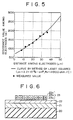
- the value of the contact specific resistance when annealing is performed at 700°C was estimated, the value showed a comparatively small value at 3.2x10 -2 ⁇ cm 2 as shown in Fig. 5.
- the method shown in "G. S. Marlow et al., Solid State Electronics 25(1982) 91" was used.
- the sheet resistance value of the p-type compound semiconductor layer 11 at this time was 14,900 ⁇ / ⁇ .
- the value of the contact specific resistance can be made smaller by the electrode layer 13 in which the transition metal layer 13a composed of nickel, the platinum layer 13b and the gold layer 13c are laminated one after another.
- thermal stability can also be increased when annealing is performed at 700°C.
- a specimen was produced similarly to the first embodiment except that the transition metal layer 13a of the first embodiment was formed of palladium. Thereafter, the change of the resistance value caused by annealing was examined similarly to the first embodiment. Besides, in order to compare with the first embodiment, that which was cut out of the same wafer as the first embodiment was used for a p-type compound semiconductor layer 11 formed on a sapphire substrate 10.
- Fig. 4 The results obtained on those that has the distance among electrodes at 24 ⁇ m are shown in Fig. 4 similarly to the first embodiment.
- the resistance value becomes smaller by annealing at 800°C, but the resistance value before annealing is performed has been the smallest.
- the resistance value before annealing is performed in a conventional example and the resistance value before annealing is performed in the present embodiment are compared with each other, it was found that the resistance value in the present embodiment was smaller.
- a specimen was produced in a similar manner as the first embodiment except that the transition metal layer 13a of the first embodiment was formed of cobalt. Thereafter, the change of resistance value caused by annealing was examined similarly to the first embodiment. Besides, in order to compare with the first embodiment, that which has been cut out of the same wafer as the first embodiment was used for a p-type compound semiconductor layer formed on a sapphire substrate 10.
- Fig. 4 The results on those that have the distance among electrodes at 24 ⁇ m are shown in Fig. 4 similarly to the first embodiment.
- the resistance value before annealing was comparatively large, the resistance value becomes the smallest by means of annealing at 700°C in the present embodiment.
- the smallest resistance value (before annealing is applied) in the conventional example and the smallest value (annealed at 700°C) in the present embodiment were compared with each other, it was found that the resistance value in the present embodiment was smaller.
- a specimen was produced in a similar manner as the first embodiment except that the transition metal layer 13a of the first embodiment was formed of titanium. Thereafter, the change of the resistance value caused by annealing was examined similarly to the first embodiment. Besides, in order to compare with the first embodiment, that which was cut out of the same wafer as the first embodiment was used for a p-type compound semiconductor layer 11 formed on a sapphire substrate 10.
- Fig. 4 The results on those that have the distance among electrodes at 24 ⁇ m are shown in Fig. 4 similarly to the first embodiment.
- the resistance value before annealing is applied has been comparatively large, the resistance value became the smallest by means of annealing at 800°C in the present embodiment.
- the smallest resistance value (before annealing is applied) in the conventional example and the smallest resistance value (annealed at 800°C) in the present embodiment were compared with each other, it was found that the resistance value in the present embodiment was smaller.
- Fig. 6 shows a structure of a specimen produced in a fifth embodiment.
- a p- type compound semiconductor layer 21 formed on a sapphire substrate 20 was prepared first in a similar manner as the first embodiment. Then, an oxide film formed on the surface thereof was removed with a mixed liquid of ammonium fluoride and hydrofluoric acid, and, the p-type compound semiconductor layer 21 on the substrate 20 was inserted into a growth chamber of an MBE growth apparatus after cleaning with pure water and drying.
- the substrate temperature was risen up to 850°C and the surface thereof was nitrided by nitrogen plasma, and a gallium beam, nitrogen plasma and a magnesium beam are radiated thereafter so as to grow GaN, thus forming a contact layer 22.
- nitrogen was excited by an Electron Cyclotron Resonance (ECR) cell or a Radio Frequency (RF) cell.
- ECR Electron Cyclotron Resonance
- RF Radio Frequency
- a transition metal layer 23a composed of nickel, a platinum layer 23b and a gold layer 23c were laminated one after another in the similar manner as the first embodiment, thereby to form an electrode layer 23.
- the contact specific resistance was 10 -3 ⁇ cm 2 or lower. Namely, it has been found that the value of the contact specific resistance could be made smaller by inserting the contact layer 22 between the p-type compound semiconductor layer 21 and the electrode layer 23.
- the present invention has been described above citing embodiments. However, the present invention is not limited to these embodiments, but may be modified in various ways within isometric range thereof.
- the contact layer 2 was inserted between the p-type compound semiconductor layer 1 and the electrode layer 3, but it is not necessarily required to insert the contact layer 2 as seen from the first to the fourth embodiments.
- transition metal layers 13a and 23a were formed of a simple substance such as nickel and palladium in the above-mentioned respective embodiments, but may be formed of an alloy with other metals.
- an electrode layer composed of a complex containing gold, platinum and at least one type among transition metal elements other than gold or platinum is provided. Therefore, it is possible to make the value of the contact specific resistance smaller and also to increase the thermal stability. Hence, such an effect that the elements can be operated stably for a long period is produced.
- an ohmic electrode related to the present invention since there are provided a process of forming a transition metal layer, a platinum layer and a gold layer one after another on a p-type compound semiconductor layer and a process of annealing thereafter, it is possible to have the platinum layer adhere closely to the p-type compound semiconductor layer by the transition metal layer while preventing gold from diffusing toward the p-type compound semiconductor layer by means of the platinum layer. Thus, it is possible to realize an ohmic electrode according to the present invention.
Abstract
Description
Claims (14)
- An ohmic electrode structure, comprising:a p-type compound semiconductor layer containing at least one type among groups composed of Ga, Al, B and In and N; andan electrode layer containing at least one type among Au, Pt and transition metal elements excluding Au and Pt on said p-type compound semiconductor layer.
- An ohmic electrode structure according to Claim 1, wherein said electrode layer is composed of a first layer containing at least one type among transition metal elements excluding Au and Pt, a second layer containing Pt and a third layer containing Au consecutively on said p-type compound semiconductor layer.
- An ohmic electrode structure according to Claim 1, wherein said electrode layer is formed of a transition metal layer containing at least one type among transition metal elements excluding Au and Pt, a Pt layer and an Au layer consecutively on said p-type compound semiconductor layer.
- An ohmic electrode structure according to Claim 1, wherein said electrode layer contains Au, Pt and Pd.
- An ohmic electrode structure according to Claim 1, wherein said electrode layer contains Au, Pt and Ni.
- An ohmic electrode structure according to Claim 1, wherein there is provided a contact layer composed of a p-type compound semiconductor containing at least one type among groups of Ga, Al, B and In and N between said p-type compound semiconductor layer and said electrode layer, and the hole density of said contact layer is higher than that of said p-type compound semiconductor layer.
- A method of forming an ohmic electrode structure, comprising the steps of:forming a first layer containing at least one type among transition metals excluding Au and Pt on a p- type compound semiconductor layer containing at least one type among groups composed of Ga, Al, B and In and N;forming a second layer containing Pt on said first layer;forming a third layer containing Au on said second layer; andapplying heat treatment to said first, second and third layers.
- A method of forming an ohmic electrode according to Claim 7, wherein said first layer contains Pd.
- A method of forming an ohmic electrode according to Claim 7, wherein said first layer contains Ni.
- A method of forming an ohmic electrode according to Claim 7, wherein said first layer is composed of Pd, said second layer is composed of Pt and said third layer is composed of Au.
- A method of forming an ohmic electrode according to Claim 7, wherein said first layer is composed of Ni, said second layer is composed of Pt, and said third layer is composed of Au.
- A method of forming an ohmic electrode according to Claim 7, wherein said first layer contains Ni, and the temperature of said heat treatment is set to 600°C to 800°C.
- A method of forming an ohmic electrode according to Claim 7, further comprising a process of forming a contact layer composed of a p-type compound semiconductor containing at least one type among groups composed of Ga, Al, B and In and N on said p-type compound semiconductor layer by means of molecular beam epitaxy prior to the process of forming said first layer.
- A semiconductor element having an ohmic electrode structure, wherein said ohmic electrode structure comprises:a p-type compound semiconductor layer containing at least one type among groups composed of Ga, Al, B and In and N; andan electrode layer containing at least one type among Au, Pt and transition metal elements excluding Au and Pt on said p-type compound semiconductor layer.
Applications Claiming Priority (3)
| Application Number | Priority Date | Filing Date | Title |
|---|---|---|---|
| JP21311796A JP3587224B2 (en) | 1996-07-24 | 1996-07-24 | Ohmic electrode |
| JP213117/96 | 1996-07-24 | ||
| JP21311796 | 1996-07-24 |
Publications (3)
| Publication Number | Publication Date |
|---|---|
| EP0825652A2 true EP0825652A2 (en) | 1998-02-25 |
| EP0825652A3 EP0825652A3 (en) | 1998-11-18 |
| EP0825652B1 EP0825652B1 (en) | 2002-02-20 |
Family
ID=16633872
Family Applications (1)
| Application Number | Title | Priority Date | Filing Date |
|---|---|---|---|
| EP97111565A Expired - Lifetime EP0825652B1 (en) | 1996-07-24 | 1997-07-08 | Ohmic electrode and method of forming the same |
Country Status (4)
| Country | Link |
|---|---|
| EP (1) | EP0825652B1 (en) |
| JP (1) | JP3587224B2 (en) |
| KR (2) | KR100496369B1 (en) |
| DE (1) | DE69710539T2 (en) |
Cited By (4)
| Publication number | Priority date | Publication date | Assignee | Title |
|---|---|---|---|---|
| US6936859B1 (en) | 1998-05-13 | 2005-08-30 | Toyoda Gosei Co., Ltd. | Light-emitting semiconductor device using group III nitride compound |
| GB2426382A (en) * | 2002-11-26 | 2006-11-22 | Gen Electric | Three-layer compound electrode for organic electronic devices |
| DE19921987B4 (en) * | 1998-05-13 | 2007-05-16 | Toyoda Gosei Kk | Light-emitting semiconductor device with group III element-nitride compounds |
| US8581279B2 (en) | 2005-06-02 | 2013-11-12 | Osram Opto Semiconductors Gmbh | Light-emitting diode chip comprising a contact structure |
Families Citing this family (6)
| Publication number | Priority date | Publication date | Assignee | Title |
|---|---|---|---|---|
| JP2000031084A (en) * | 1998-05-08 | 2000-01-28 | Samsung Electron Co Ltd | Activation method of compound semiconductor thin film to p-type |
| KR100459885B1 (en) * | 1998-11-05 | 2005-01-15 | 삼성전자주식회사 | Method for forming a metal electrode on the semiconductor |
| KR101023115B1 (en) * | 2003-11-13 | 2011-03-24 | 주식회사 포스코 | Door apparatus of heating furnace |
| TWI224877B (en) * | 2003-12-25 | 2004-12-01 | Super Nova Optoelectronics Cor | Gallium nitride series light-emitting diode structure and its manufacturing method |
| WO2005071763A2 (en) | 2004-01-26 | 2005-08-04 | Osram Opto Semiconductors Gmbh | Thin-film led comprising a current-dispersing structure |
| JP4197030B2 (en) | 2006-11-09 | 2008-12-17 | ソニー株式会社 | Semiconductor laser, semiconductor laser manufacturing method, optical pickup, and optical disc apparatus |
Citations (1)
| Publication number | Priority date | Publication date | Assignee | Title |
|---|---|---|---|---|
| JPH07254732A (en) * | 1994-03-15 | 1995-10-03 | Toshiba Corp | Semiconductor light emitting device |
Family Cites Families (20)
| Publication number | Priority date | Publication date | Assignee | Title |
|---|---|---|---|---|
| JPS5727056A (en) * | 1980-07-25 | 1982-02-13 | Nec Corp | Semiconductor device |
| JPS6189664A (en) * | 1984-10-09 | 1986-05-07 | Fujitsu Ltd | Manufacture of semiconductor device |
| JPS6197890A (en) * | 1984-10-18 | 1986-05-16 | Fujitsu Ltd | Semiconductor device |
| JPS61251184A (en) * | 1985-04-30 | 1986-11-08 | Fujitsu Ltd | Manufacture of semiconductor device |
| JPS635519A (en) * | 1986-06-25 | 1988-01-11 | Nec Corp | Formation of semiconductor electrode |
| JPH04363020A (en) * | 1990-11-28 | 1992-12-15 | Toshiba Corp | Manufacture of semiconductor device |
| JPH04291979A (en) * | 1991-03-20 | 1992-10-16 | Fujitsu Ltd | Fabrication of semiconductor light emitting device |
| JP3247437B2 (en) * | 1992-03-10 | 2002-01-15 | 旭化成株式会社 | Nitride-based semiconductor device and method of manufacturing the same |
| JP2778349B2 (en) * | 1992-04-10 | 1998-07-23 | 日亜化学工業株式会社 | Gallium nitride based compound semiconductor electrodes |
| JPH05335622A (en) * | 1992-05-27 | 1993-12-17 | Asahi Chem Ind Co Ltd | Semiconductor light-emitting device |
| JPH0669546A (en) * | 1992-08-21 | 1994-03-11 | Asahi Chem Ind Co Ltd | Light-emitting diode |
| JPH0677537A (en) * | 1992-08-24 | 1994-03-18 | Asahi Chem Ind Co Ltd | Light emitting diode |
| JP2803742B2 (en) * | 1993-04-28 | 1998-09-24 | 日亜化学工業株式会社 | Gallium nitride-based compound semiconductor light emitting device and method for forming electrode thereof |
| JP2803741B2 (en) * | 1993-03-19 | 1998-09-24 | 日亜化学工業株式会社 | Gallium nitride based compound semiconductor electrode forming method |
| JP3293996B2 (en) * | 1994-03-15 | 2002-06-17 | 株式会社東芝 | Semiconductor device |
| JPH0832115A (en) * | 1994-07-19 | 1996-02-02 | Sharp Corp | Electrode structure and its manufacture |
| JP3620926B2 (en) * | 1995-06-16 | 2005-02-16 | 豊田合成株式会社 | P-conducting group III nitride semiconductor electrode, electrode forming method and device |
| JP3669091B2 (en) * | 1996-01-09 | 2005-07-06 | 住友化学株式会社 | Method for producing electrode for group 3-5 compound semiconductor |
| JP3233258B2 (en) * | 1996-04-24 | 2001-11-26 | 日亜化学工業株式会社 | Nitride semiconductor electrode |
| JP3579294B2 (en) * | 1999-04-19 | 2004-10-20 | シャープ株式会社 | Electrode manufacturing method |
-
1996
- 1996-07-24 JP JP21311796A patent/JP3587224B2/en not_active Expired - Lifetime
-
1997
- 1997-07-08 DE DE69710539T patent/DE69710539T2/en not_active Expired - Lifetime
- 1997-07-08 EP EP97111565A patent/EP0825652B1/en not_active Expired - Lifetime
- 1997-07-23 KR KR1019970034396A patent/KR100496369B1/en not_active IP Right Cessation
-
2004
- 2004-10-26 KR KR1020040085607A patent/KR100537398B1/en not_active IP Right Cessation
Patent Citations (1)
| Publication number | Priority date | Publication date | Assignee | Title |
|---|---|---|---|---|
| JPH07254732A (en) * | 1994-03-15 | 1995-10-03 | Toshiba Corp | Semiconductor light emitting device |
Non-Patent Citations (4)
| Title |
|---|
| KING D J ET AL: "Temperature behavior of Pt/Au ohmic contacts to p-GaN" GALLIUM NITRIDE AND RELATED MATERIALS II. SYMPOSIUM, GALLIUM NITRIDE AND RELATED MATERIALS II. SYMPOSIUM, SAN FRANCISCO, CA, USA, 1-4 APRIL 1997, 1997, PITTSBURGH, PA, USA, MATER. RES. SOC, USA, pages 421-426, XP002077829 * |
| MOLNAR R J ET AL: "BLUE-VIOLET LIGHT EMITTING GALLIUM NITRIDE P-N JUNCTIONS GROWN BY ELECTRON CYCLOTRON RESONANCE-ASSISTED MOLECULAR BEAM EPITAXY" APPLIED PHYSICS LETTERS, vol. 66, no. 3, 16 January 1995, pages 268-270, XP000486024 * |
| NAKAMURA S ET AL: "CANDELA-CLASS HIGH-BRIGHTNESS INGAN/AIGAN DOUBLE-HETEROSTRUCTURE BLUE-LIGHT-EMITTING DIODES" APPLIED PHYSICS LETTERS, vol. 64, no. 13, 28 March 1994, pages 1687-1689, XP000441256 * |
| SMITH M A ET AL: "AN INVESTIGATION OF REFRACTORY METAL OHMIC CONTACTS TO GALLIUM NITRIDE" PROCEEDINGS OF THE FIRST SYMPOSIUM ON III-V NITRIDE MATERIALS AND PROCESSES, PROCEEDINGS OF III-V NITRIDE MATERIALS AND PROCESSES. (ISBN 1 56677 163 3), LOS ANGELES, CA, USA, 6-8 MAY 1996, 1996, PENNINGTON, NJ, USA, ELECTROCHEM. SOC, USA, pages 133-141, XP002077828 * |
Cited By (6)
| Publication number | Priority date | Publication date | Assignee | Title |
|---|---|---|---|---|
| US6936859B1 (en) | 1998-05-13 | 2005-08-30 | Toyoda Gosei Co., Ltd. | Light-emitting semiconductor device using group III nitride compound |
| US7109529B2 (en) | 1998-05-13 | 2006-09-19 | Toyoda Gosei Co., Ltd. | Light-emitting semiconductor device using group III nitride compound |
| DE19921987B4 (en) * | 1998-05-13 | 2007-05-16 | Toyoda Gosei Kk | Light-emitting semiconductor device with group III element-nitride compounds |
| GB2426382A (en) * | 2002-11-26 | 2006-11-22 | Gen Electric | Three-layer compound electrode for organic electronic devices |
| GB2426382B (en) * | 2002-11-26 | 2007-07-04 | Gen Electric | Electrodes mitigating effcts of defects in organic electronic devices |
| US8581279B2 (en) | 2005-06-02 | 2013-11-12 | Osram Opto Semiconductors Gmbh | Light-emitting diode chip comprising a contact structure |
Also Published As
| Publication number | Publication date |
|---|---|
| JPH1041254A (en) | 1998-02-13 |
| KR100496369B1 (en) | 2005-09-08 |
| KR980011940A (en) | 1998-04-30 |
| KR100537398B1 (en) | 2005-12-19 |
| EP0825652A3 (en) | 1998-11-18 |
| DE69710539T2 (en) | 2002-10-31 |
| DE69710539D1 (en) | 2002-03-28 |
| JP3587224B2 (en) | 2004-11-10 |
| EP0825652B1 (en) | 2002-02-20 |
Similar Documents
| Publication | Publication Date | Title |
|---|---|---|
| Fan et al. | Very low resistance multilayer Ohmic contact to n‐GaN | |
| Pearton et al. | GaN: Processing, defects, and devices | |
| EP0881666B2 (en) | P-type nitrogen compound semiconductor and method of manufacturing same | |
| JP2786952B2 (en) | Gallium nitride based compound semiconductor light emitting device and method of manufacturing the same | |
| US6100174A (en) | GaN group compound semiconductor device and method for producing the same | |
| JP3705016B2 (en) | Translucent electrode film and group III nitride compound semiconductor device | |
| US7973338B2 (en) | Hetero junction field effect transistor and method of fabricating the same | |
| US7253015B2 (en) | Low doped layer for nitride-based semiconductor device | |
| US6248607B1 (en) | Method for manufacturing semiconductor light emitting device | |
| EP0825652B1 (en) | Ohmic electrode and method of forming the same | |
| JP2884083B1 (en) | Method of forming semiconductor layer epitaxially grown on metal layer and light emitting semiconductor device manufactured using this method | |
| JP4494567B2 (en) | Method of forming electrode on n-type gallium nitride compound semiconductor layer | |
| US20040023423A1 (en) | Semiconductor layer formed by selective deposition and method for depositing semiconductor layer | |
| US6388323B1 (en) | Electrode material and electrode for III-V group compound semiconductor | |
| JP3497790B2 (en) | Method for manufacturing p-type gallium nitride based semiconductor and light emitting device using p-type gallium nitride based semiconductor | |
| KR100387099B1 (en) | GaN-Based Light Emitting Diode and Fabrication Method thereof | |
| Nikolaev et al. | GaN pn-structures grown by hydride vapor phase epitaxy | |
| JPH10189944A (en) | High electron-mobility transistor | |
| JP3792003B2 (en) | Semiconductor light emitting device | |
| JPH11274567A (en) | Method for forming electrode of semiconductor element | |
| KR100293467B1 (en) | blue emitting device and method for fabricating the same | |
| JP4123200B2 (en) | Method for forming ohmic electrode | |
| JP3384700B2 (en) | Gallium nitride based compound semiconductor light emitting device and method of manufacturing the same | |
| KR100348280B1 (en) | method for fabricating blue emitting device | |
| JPH05275467A (en) | Manufacture of compound semiconductor device |
Legal Events
| Date | Code | Title | Description |
|---|---|---|---|
| PUAI | Public reference made under article 153(3) epc to a published international application that has entered the european phase |
Free format text: ORIGINAL CODE: 0009012 |
|
| AK | Designated contracting states |
Kind code of ref document: A2 Designated state(s): DE FR GB |
|
| AX | Request for extension of the european patent |
Free format text: AL;LT;LV;RO;SI |
|
| PUAL | Search report despatched |
Free format text: ORIGINAL CODE: 0009013 |
|
| AK | Designated contracting states |
Kind code of ref document: A3 Designated state(s): AT BE CH DE DK ES FI FR GB GR IE IT LI LU MC NL PT SE |
|
| AX | Request for extension of the european patent |
Free format text: AL;LT;LV;RO;SI |
|
| 17P | Request for examination filed |
Effective date: 19990420 |
|
| AKX | Designation fees paid |
Free format text: DE FR GB |
|
| 17Q | First examination report despatched |
Effective date: 19990525 |
|
| GRAG | Despatch of communication of intention to grant |
Free format text: ORIGINAL CODE: EPIDOS AGRA |
|
| GRAG | Despatch of communication of intention to grant |
Free format text: ORIGINAL CODE: EPIDOS AGRA |
|
| GRAG | Despatch of communication of intention to grant |
Free format text: ORIGINAL CODE: EPIDOS AGRA |
|
| GRAH | Despatch of communication of intention to grant a patent |
Free format text: ORIGINAL CODE: EPIDOS IGRA |
|
| GRAG | Despatch of communication of intention to grant |
Free format text: ORIGINAL CODE: EPIDOS AGRA |
|
| GRAH | Despatch of communication of intention to grant a patent |
Free format text: ORIGINAL CODE: EPIDOS IGRA |
|
| GRAH | Despatch of communication of intention to grant a patent |
Free format text: ORIGINAL CODE: EPIDOS IGRA |
|
| REG | Reference to a national code |
Ref country code: GB Ref legal event code: IF02 |
|
| GRAA | (expected) grant |
Free format text: ORIGINAL CODE: 0009210 |
|
| AK | Designated contracting states |
Kind code of ref document: B1 Designated state(s): DE FR GB |
|
| REF | Corresponds to: |
Ref document number: 69710539 Country of ref document: DE Date of ref document: 20020328 |
|
| ET | Fr: translation filed | ||
| PLBE | No opposition filed within time limit |
Free format text: ORIGINAL CODE: 0009261 |
|
| STAA | Information on the status of an ep patent application or granted ep patent |
Free format text: STATUS: NO OPPOSITION FILED WITHIN TIME LIMIT |
|
| 26N | No opposition filed |
Effective date: 20021121 |
|
| REG | Reference to a national code |
Ref country code: GB Ref legal event code: 746 Effective date: 20120703 |
|
| REG | Reference to a national code |
Ref country code: DE Ref legal event code: R084 Ref document number: 69710539 Country of ref document: DE Effective date: 20120614 |
|
| REG | Reference to a national code |
Ref country code: FR Ref legal event code: PLFP Year of fee payment: 20 |
|
| PGFP | Annual fee paid to national office [announced via postgrant information from national office to epo] |
Ref country code: DE Payment date: 20160722 Year of fee payment: 20 Ref country code: GB Payment date: 20160721 Year of fee payment: 20 |
|
| PGFP | Annual fee paid to national office [announced via postgrant information from national office to epo] |
Ref country code: FR Payment date: 20160721 Year of fee payment: 20 |
|
| REG | Reference to a national code |
Ref country code: DE Ref legal event code: R071 Ref document number: 69710539 Country of ref document: DE |
|
| REG | Reference to a national code |
Ref country code: GB Ref legal event code: PE20 Expiry date: 20170707 |
|
| PG25 | Lapsed in a contracting state [announced via postgrant information from national office to epo] |
Ref country code: GB Free format text: LAPSE BECAUSE OF EXPIRATION OF PROTECTION Effective date: 20170707 |