EP0593924A1 - Device for producing plasma using cathodic sputtering - Google Patents
Device for producing plasma using cathodic sputtering Download PDFInfo
- Publication number
- EP0593924A1 EP0593924A1 EP93115314A EP93115314A EP0593924A1 EP 0593924 A1 EP0593924 A1 EP 0593924A1 EP 93115314 A EP93115314 A EP 93115314A EP 93115314 A EP93115314 A EP 93115314A EP 0593924 A1 EP0593924 A1 EP 0593924A1
- Authority
- EP
- European Patent Office
- Prior art keywords
- coil
- target
- plasma
- shielding plates
- frequency
- Prior art date
- Legal status (The legal status is an assumption and is not a legal conclusion. Google has not performed a legal analysis and makes no representation as to the accuracy of the status listed.)
- Granted
Links
Images

Classifications
-
- H—ELECTRICITY
- H01—ELECTRIC ELEMENTS
- H01J—ELECTRIC DISCHARGE TUBES OR DISCHARGE LAMPS
- H01J37/00—Discharge tubes with provision for introducing objects or material to be exposed to the discharge, e.g. for the purpose of examination or processing thereof
- H01J37/32—Gas-filled discharge tubes
- H01J37/32009—Arrangements for generation of plasma specially adapted for examination or treatment of objects, e.g. plasma sources
- H01J37/32082—Radio frequency generated discharge
- H01J37/321—Radio frequency generated discharge the radio frequency energy being inductively coupled to the plasma
- H01J37/3211—Antennas, e.g. particular shapes of coils
-
- H—ELECTRICITY
- H01—ELECTRIC ELEMENTS
- H01J—ELECTRIC DISCHARGE TUBES OR DISCHARGE LAMPS
- H01J37/00—Discharge tubes with provision for introducing objects or material to be exposed to the discharge, e.g. for the purpose of examination or processing thereof
- H01J37/32—Gas-filled discharge tubes
- H01J37/32009—Arrangements for generation of plasma specially adapted for examination or treatment of objects, e.g. plasma sources
- H01J37/32082—Radio frequency generated discharge
- H01J37/321—Radio frequency generated discharge the radio frequency energy being inductively coupled to the plasma
-
- H—ELECTRICITY
- H01—ELECTRIC ELEMENTS
- H01J—ELECTRIC DISCHARGE TUBES OR DISCHARGE LAMPS
- H01J37/00—Discharge tubes with provision for introducing objects or material to be exposed to the discharge, e.g. for the purpose of examination or processing thereof
- H01J37/32—Gas-filled discharge tubes
- H01J37/34—Gas-filled discharge tubes operating with cathodic sputtering
- H01J37/3402—Gas-filled discharge tubes operating with cathodic sputtering using supplementary magnetic fields
- H01J37/3405—Magnetron sputtering
-
- H—ELECTRICITY
- H01—ELECTRIC ELEMENTS
- H01J—ELECTRIC DISCHARGE TUBES OR DISCHARGE LAMPS
- H01J37/00—Discharge tubes with provision for introducing objects or material to be exposed to the discharge, e.g. for the purpose of examination or processing thereof
- H01J37/32—Gas-filled discharge tubes
- H01J37/34—Gas-filled discharge tubes operating with cathodic sputtering
- H01J37/3411—Constructional aspects of the reactor
- H01J37/3414—Targets
Definitions
- the invention relates to a device for generating a plasma by means of sputtering according to the preamble of claim 1.
- a high-frequency generator which transmits 13.56 MHz waves along a magnetic field which enters the discharge space through an external magnetic field generator (US Pat. No. 4,990,229).
- an external magnetic field generator US Pat. No. 4,990,229
- Helicon-Whistler waves in a plasma space are excited, which lead to a particularly high one Lead plasma activation.
- special antenna structures are provided.
- the disadvantage of the known device is that although it can be used to generate a highly activated and highly ionized plasma, it is not possible to carry out a sputter coating.
- a sputter system which has a high-frequency excitation coil with four turns, which is arranged between a disk-shaped target and a substrate holder in a conventional DC diode system (Matsuo Yamashita: "Effect of magnetic field on plasma characteristics of built- in high-frequency coil type sputtering apparatus ", J. Vac. Sci. Technol. A 7 (4), Jul / Aug 1989, pp. 2752-2757).
- a static magnetic field that penetrates into the plasma area also runs perpendicular to the axis of the high-frequency excitation coil. However, it is not possible to generate Whistler waves with this sputtering system.
- the object of the invention is to apply an RF wave to the plasma space of a magnetron cathode in such a way that Whistler waves can form.
- the advantage achieved with the invention is, in particular, that, owing to a higher volume efficiency, a significantly higher degree of ionization than with conventional devices can be achieved.
- the excitation of Whistler waves in the plasma ionizes the plasma particularly effectively. But also without excitation of "Whistler waves", i.e. H. with normal excitation, a higher degree of plasma ionization is generated than in systems in which there is no wave coupling.
- the invention combines the high plasma density and the sputter coating with one another.
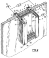
- a plasma chamber 1 shows a section of a plasma chamber 1, which is surrounded by a housing 2.
- a substrate 3 In the lower area of the housing 2 there is a substrate 3 on a turntable 4.
- a magnetron cathode 5 Above the substrate 3, which is to be etched or coated, a magnetron cathode 5 is provided, which in turn has three permanent magnets 6, 7, 8, a yoke 9 and a cathode tub 10 has.
- the cathode tub 10 rests on insulators 11, 12 which are provided with seals 13, 14. These insulators 11, 12 are embedded in the top of the housing 2.
- the negative pole of a direct current supply 15, the positive pole of which is connected to the housing mass of the recipient 2 lies on the electrode trough 10.
- a high-frequency supply 16 can also be provided.
- Beneath the cathode trough 10 there is a target 17 through which the magnetic field lines 18, 19 of the permanent magnets 6 to 8 pass.
- An L-shaped shield 20, 21
- the coil 24 is a coil for generating an additional magnetic field in the plasma space. It is preferably operated with direct current.
- An insulator 26, 27 is provided in front of the vertical part 22, 23 and has grooves in which there is a further coil 28 which is connected to a high-frequency source 29.
- the insulator 26, 27 is closed on its underside by a horizontal part 30, 31 behind the shield 20, 21.
- This part of the shield 20, 21 is electrically insulated and can either be grounded or connected to any electrical potential. It represents the effective anode of the device and can also be used as a distribution screen.
- a cover plate 32, 33 made of an insulating material, for.
- the high-frequency source 29 uses the antenna coil 28 to generate electromagnetic waves in the plasma space, which become Whistler waves can train. The interaction of the electromagnetic waves of the coil 28 with the field of the coil 24 leads to the excitation of helicon modes in the plasma.
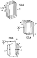
- Fig. 2 shows the magnetron cathode 5 with the shield 20, 21 and the two coils 24 and 28. It can be seen clearly that the coils 24, 28 are embedded in the shield 20, 21 or wrap them around such that the Magnetic fields arising when current flows through are perpendicular to the target 17.
- the substrate 3 and the turntable 4 are omitted in FIG. 2.
- the supply sources 25 and 29 are shown inside the housing 2, although they are actually outside this housing 2, as shown in FIG. 1.
- FIG. 3 to 5 show a more detailed illustration of the high-frequency coil 28.
- the coil 28 is wound clockwise and has one end connected to ground or earth, while its other end 36 is connected to the high-frequency source 29.
- both ends 35, 36 of the coil 28 are connected to earth or ground, while the high-frequency source 29 is connected to the center of the coil 28.
- the coil 28 is divided into two halves 40, 41, the winding direction of these two halves 40, 41 being opposite. Both halves are embedded in the grooves of an insulator at a certain distance from one another. One of these halves 40 is embedded in the insulator part 26, while the other half 41 lies in the grooves of the insulator part 27.
- the winding direction of the coil halves 40, 41 is such that their magnetic fields run parallel to the surface of the target 17.
- D is the slot width, while a is the distance between the coil sections 40, 41.
Abstract
Description
Die Erfindung betrifft eine Vorrichtung zum Erzeugen eines Plasmas mittels Kathodenzerstäubung nach dem Oberbegriff des Patentanspruchs 1.The invention relates to a device for generating a plasma by means of sputtering according to the preamble of claim 1.
Auf zahlreichen Gebieten der Technik ist es erforderlich, dünne Schichten auf Substrate aufzubringen. Beispielsweise werden Glasscheiben beschichtet, um ihnen zu besonderen Eigenschaften zu verhelfen, oder es werden Uhrengehäuse aus einem weniger edlen Material mit einer aus edlem Material bestehenden Schicht überzogen.In many areas of technology, it is necessary to apply thin layers to substrates. For example, glass panes are coated to give them special properties, or watch cases made of a less noble material are coated with a layer made of noble material.
Für das Aufbringen dünner Schichten auf Substrate sind bereits zahlreiche Verfahren vorgeschlagen worden, von denen lediglich die Galvanotechnik und das Beschichten aus einem Plasma heraus erwähnt seien. Das Beschichten aus dem Plasma hat in den letzten Jahren immer mehr an Bedeutung gewonnen, weil es eine Vielzahl von Materialien als Beschichtungsmaterial zuläßt.Numerous methods have already been proposed for applying thin layers to substrates, of which only the electroplating technology and the coating from a plasma should be mentioned. Coating from plasma has become increasingly important in recent years because it allows a large number of materials as coating material.
Um ein für die Beschichtung geeignetes Plasma herzustellen, sind ebenfalls verschiedene Verfahren vorgeschlagen worden. Von diesen Verfahren ist das Kathodenzerstäubungsverfahren, das auch Sputtern genannt wird, wegen seiner hohen Beschichtungsraten von großem Interesse.Various methods have also been proposed to produce a plasma suitable for the coating. Of these processes, the sputtering process, also called sputtering, is of great interest because of its high coating rates.
Bei einer bekannten Vorrichtung für die Erzeugung eines Plasmas hoher Dichte kommt ein Hochfrequenz-Generator zum Einsatz, der 13,56 MHz-Wellen entlang eines Magnetfelds sendet, welches durch einen externen Magnetfeldgenerator in den Entladungsraum gelangt (US-PS 4 990 229). Mit Hilfe dieser Vorrichtung werden Helicon-Whistler-Wellen in einem Plasmaraum angeregt, die zu einer besonders hohen Plasmaaktivierung führen. Um bestimmte Wellenmoden für Whistler-Wellen anzuregen, sind besondere Antennenstrukturen vorgesehen. Eine Antenne für die Anregung von Whistler-Wellen ist bei einer Anregungsfrequenz von 13,56 MHz derart ausgelegt, daß sie die m = 0 und m = 1 Moden anregt.In a known device for generating a high-density plasma, a high-frequency generator is used which transmits 13.56 MHz waves along a magnetic field which enters the discharge space through an external magnetic field generator (US Pat. No. 4,990,229). With the help of this device, Helicon-Whistler waves in a plasma space are excited, which lead to a particularly high one Lead plasma activation. In order to excite certain wave modes for Whistler waves, special antenna structures are provided. An antenna for the excitation of Whistler waves is designed at an excitation frequency of 13.56 MHz in such a way that it excites the m = 0 and m = 1 modes.
Der Nachteil der bekannten Vorrichtung besteht darin, daß mit ihr zwar ein hochaktiviertes und hochionisiertes Plasma erzeugt werden kann, daß es jedoch nicht möglich ist, eine Sputterbeschichtung durchzuführen.The disadvantage of the known device is that although it can be used to generate a highly activated and highly ionized plasma, it is not possible to carry out a sputter coating.
Es ist weiterhin eine Sputteranlage bekannt, die eine Hochfrequenz-Anregungsspule mit vier Windungen aufweist, welche zwischen einem scheibenförmigen Target und einem Substrathalter in einer herkömmlichen DC-Dioden-Anlage angeordnet ist (Matsuo Yamashita: "Effect of magnetic field on plasma characteristics of built-in high-frequency coil type sputtering apparatus", J. Vac. Sci. Technol. A 7 (4), Jul/Aug 1989, S. 2752 - 2757). Senkrecht zur Achse der Hochfrequenz-Anregungsspule verläuft außerdem ein statisches Magnetfeld, das in den Plasmabereich eindringt. Mit dieser Sputteranlage ist es indessen nicht möglich, Whistler-Wellen zu erzeugen.A sputter system is also known which has a high-frequency excitation coil with four turns, which is arranged between a disk-shaped target and a substrate holder in a conventional DC diode system (Matsuo Yamashita: "Effect of magnetic field on plasma characteristics of built- in high-frequency coil type sputtering apparatus ", J. Vac. Sci. Technol. A 7 (4), Jul / Aug 1989, pp. 2752-2757). A static magnetic field that penetrates into the plasma area also runs perpendicular to the axis of the high-frequency excitation coil. However, it is not possible to generate Whistler waves with this sputtering system.
Der Erfindung liegt die Aufgabe zugrunde, den Plasmaraum einer Magnetron-Kathode derart mit einer HF-Welle zu beaufschlagen, daß sich Whistler-Wellen ausbilden können.The object of the invention is to apply an RF wave to the plasma space of a magnetron cathode in such a way that Whistler waves can form.
Diese Aufgabe wird gemäß den Merkmalen des Patentanspruchs 1 gelöst.This object is achieved in accordance with the features of patent claim 1.
Der mit der Erfindung erzielte Vorteil besteht insbesondere darin, daß aufgrund einer höheren Volumenwirksamkeit ein wesentlich höherer Ionisationsgrad als bei herkömmlichen Vorrichtungen erzielt werden kann. Durch die Anregung von Whistler-Wellen im Plasma wird das Plasma besonders effektiv ionisiert. Aber auch ohne Anregung von "Whistler-Wellen", d. h. bei normaler Anregung, wird ein höherer Plasmaionisationsgrad erzeugt als bei Anlagen, in denen keine Welleneinkopplung erfolgt. Durch die Erfindung werden die hohe Plasmadichte und die Sputterbeschichtung miteinander kombiniert.The advantage achieved with the invention is, in particular, that, owing to a higher volume efficiency, a significantly higher degree of ionization than with conventional devices can be achieved. The excitation of Whistler waves in the plasma ionizes the plasma particularly effectively. But also without excitation of "Whistler waves", i.e. H. with normal excitation, a higher degree of plasma ionization is generated than in systems in which there is no wave coupling. The invention combines the high plasma density and the sputter coating with one another.
Ein Ausführungsbeispiel der Erfindung ist in der Zeichnung dargestellt und wird im folgenden näher beschrieben. Es zeigen:
- Fig. 1
- eine Plasmakammer mit einer Magnetronkathode und einer Spulenantenne;
- Fig. 2
- eine perspektivische Ansicht der Magnetronkathode und der Spulenantenne gemäß Fig. 1;
- Fig. 3
- eine erste Hochfrequenzspulenvorrichtung;
- Fig. 4
- eine zweite Hochfrequenzspulenvorrichtung;
- Fig. 5
- eine dritte Hochfrequenzspulenvorrichtung.
- Fig. 1
- a plasma chamber with a magnetron cathode and a coil antenna;
- Fig. 2
- a perspective view of the magnetron cathode and the coil antenna of FIG. 1;
- Fig. 3
- a first high frequency coil device;
- Fig. 4
- a second high frequency coil device;
- Fig. 5
- a third high frequency coil device.
In der Fig. 1 ist ein Ausschnitt aus einer Plasmakammer 1 gezeigt, die von einem Gehäuse 2 umgeben ist. Im unteren Bereich des Gehäuses 2 befindet sich ein Substrat 3 auf einem Drehteller 4. Oberhalb des Substrats 3, das geätzt oder beschichtet werden soll, ist eine Magnetronkathode 5 vorgesehen, die ihrerseits drei Dauermagnete 6, 7, 8, ein Joch 9 sowie eine Kathodenwanne 10 aufweist. Die Kathodenwanne 10 ruht auf Isolatoren 11, 12, die mit Dichtungen 13, 14 versehen sind. Diese Isolatoren 11, 12 sind in die Oberseite des Gehäuses 2 eingebettet. An der Elektrodenwanne 10 liegt der Minuspol einer Gleichstromversorgung 15, deren Pluspol mit der Gehäusemasse des Rezipienten 2 verbunden ist. Alternativ zur Gleichstromversorgung 15 kann auch noch eine Hochfrequenzversorgung 16 vorgesehen sein. Unterhalb der Kathodenwanne 10 befindet sich ein Target 17, durch das die Magnetfeldlinien 18, 19 der Dauermagnete 6 bis 8 stoßen. Zu beiden Seiten des Targets 17 ist eine L-förmige Abschirmung 20, 21 angeordnet.1 shows a section of a plasma chamber 1, which is surrounded by a
Um den vertikalen Teil 22, 23 der Abschirmung 20, 21 ist eine Spule 24 gewickelt, die an einer Gleichspannungsquelle 25 liegt. Die Spule 24 ist eine Spule für die Erzeugung eines zusätzlichen Magnetfelds im Plasmaraum. Sie wird bevorzugt mit Gleichstrom betrieben. Vor dem vertikalen Teil 22, 23 ist ein Isolator 26, 27 vorgesehen, der Nuten aufweist, in denen sich eine weitere Spule 28 befindet, die an eine Hochfrequenzquelle 29 angeschlossen ist. Der Isolator 26, 27 wird auf seiner Unterseite durch einen horizontalen Teil 30, 31 hinter der Abschirmung 20, 21 abgeschlossen. Dieser Teil der Abschirmung 20, 21 ist elektrisch isoliert und kann entweder geerdet oder auf ein beliebiges elektrisches Potential gelegt werden. Er stellt die effektive Anode der Vorrichtung dar und kann gleichzeitig als Verteilungsblende genutzt werden. Vor der als Antenne wirkenden Spule 28 ist eine Abdeckplatte 32, 33 aus einem isolierenden Material, z. B. aus Glas oder aus Metall, angeordnet. Im Falle einer metallenen Abdeckplatte ist diese isoliert angebracht und kann entweder elektrisch floatend sein oder von außen mit einer beliebigen Spannung beaufschlagt werden. Die Hochfrequenzquelle 29 erzeugt mittels der Antennenspule 28 im Plasmaraum elektromagnetische Wellen, die sich zu Whistler-Wellen ausbilden können. Durch das Zusammenspiel der elektromagnetischen Wellen der Spule 28 mit dem Feld der Spule 24 kommt es zur Anregung von Helicon-Moden im Plasma.A
Die Fig. 2 zeigt die Magnetronkathode 5 mit der Abschirmung 20, 21 und den beiden Spulen 24 und 28. Man erkennt hierbei deutlich, daß die Spulen 24, 28 derart in die Abschirmung 20, 21 eingebettet sind bzw. diese derart umschlingen, daß die bei Stromdurchfluß entstehenden Magnetfelder senkrecht auf dem Target 17 stehen. Das Substrat 3 und der Drehteller 4 sind in der Fig. 2 weggelassen. Die Versorgungsquellen 25 und 29 sind innerhalb des Gehäuses 2 dargestellt, obwohl sie sich in Wirklichkeit außerhalb dieses Gehäuses 2 befinden, wie es die Fig. 1 zeigt.Fig. 2 shows the
Eine genauere Darstellung der Hochfrequenzspule 28 zeigen die Fig. 3 bis 5. In der Fig. 3 ist die Spule 28 im Uhrzeigersinn gewickelt und mit ihrem einen Ende an Masse oder Erde gelegt, während ihr anderes Ende 36 mit der Hochfrequenzquelle 29 verbunden ist.3 to 5 show a more detailed illustration of the high-
Bei der Spulenanordnung gemäß Fig. 4 sind beide Enden 35, 36 der Spule 28 an Erde oder Masse gelegt, während die Hochfrequenzquelle 29 an die Mitte der Spule 28 angeschlossen ist.4, both ends 35, 36 of the
In der Fig. 5 ist die Spule 28 in zwei Hälften 40, 41 unterteilt, wobei der Wickelsinn dieser beiden Hälften 40, 41 entgegengesetzt ist. Beide Hälften sind in einem bestimmten Abstand voneinander in die Nuten eines Isolators eingebettet. Die eine dieser Hälften 40 liegt in dem Isolatorteil 26 eingebettet, während die andere Hälfte 41 in den Nuten des Isolatorteils 27 liegt. Der Wickelsinn der Spulenhälften 40, 41 ist dabei derart, daß ihre Magnetfelder parallel zur Oberfläche des Targets 17 verlaufen. Mit d ist die Nutbreite bezeichnet, während mit a der Abstand zwischen den Spulenteilstücken 40, 41 bezeichnet ist.5, the
Claims (12)
gekennzeichnet durch,
marked by,
Applications Claiming Priority (2)
| Application Number | Priority Date | Filing Date | Title |
|---|---|---|---|
| DE4235064A DE4235064A1 (en) | 1992-10-17 | 1992-10-17 | Device for generating a plasma by means of sputtering |
| DE4235064 | 1992-10-17 |
Publications (2)
| Publication Number | Publication Date |
|---|---|
| EP0593924A1 true EP0593924A1 (en) | 1994-04-27 |
| EP0593924B1 EP0593924B1 (en) | 1996-02-28 |
Family
ID=6470713
Family Applications (1)
| Application Number | Title | Priority Date | Filing Date |
|---|---|---|---|
| EP93115314A Expired - Lifetime EP0593924B1 (en) | 1992-10-17 | 1993-09-23 | Device for producing plasma using cathodic sputtering |
Country Status (5)
| Country | Link |
|---|---|
| US (1) | US5417834A (en) |
| EP (1) | EP0593924B1 (en) |
| JP (1) | JP3516054B2 (en) |
| KR (1) | KR100228534B1 (en) |
| DE (2) | DE4235064A1 (en) |
Cited By (21)
| Publication number | Priority date | Publication date | Assignee | Title |
|---|---|---|---|---|
| EP0648069A1 (en) * | 1993-07-30 | 1995-04-12 | Texas Instruments Incorporated | RF induction plasma source for plasma processing |
| WO1996018208A1 (en) * | 1994-12-06 | 1996-06-13 | Lam Research Corporation | Plasma processor for large workpieces |
| EP0727923A1 (en) * | 1995-02-15 | 1996-08-21 | Applied Materials, Inc. | Modifications in or relating to RF plasma reactors and methods of operation thereof |
| DE19518374A1 (en) * | 1995-05-23 | 1996-11-28 | Forschungszentrum Juelich Gmbh | Process for high frequency powered magnetron glow discharge ionization, as well as ion source |
| WO1997042648A1 (en) * | 1996-05-09 | 1997-11-13 | Applied Materials, Inc. | Recessed coil for generating a plasma |
| EP0836219A2 (en) * | 1996-10-08 | 1998-04-15 | Applied Materials, Inc. | Active shield for generating a plasma for sputtering |
| EP0836218A2 (en) * | 1996-10-08 | 1998-04-15 | Applied Materials, Inc. | Active shield for generating a plasma for sputtering |
| EP0837490A2 (en) * | 1996-10-17 | 1998-04-22 | Applied Materials, Inc. | A method to eliminate coil sputtering in an inductively coupled plasma (ICP) source |
| EP0841683A2 (en) * | 1996-10-08 | 1998-05-13 | Applied Materials, Inc. | Active shield for generating a plasma for sputtering |
| WO1998048444A1 (en) * | 1997-04-21 | 1998-10-29 | Tokyo Electron Arizona, Inc. | Method and apparatus for ionized sputtering of materials |
| US5948215A (en) * | 1997-04-21 | 1999-09-07 | Tokyo Electron Limited | Method and apparatus for ionized sputtering |
| US6080287A (en) * | 1998-05-06 | 2000-06-27 | Tokyo Electron Limited | Method and apparatus for ionized physical vapor deposition |
| US6190513B1 (en) | 1997-05-14 | 2001-02-20 | Applied Materials, Inc. | Darkspace shield for improved RF transmission in inductively coupled plasma sources for sputter deposition |
| US6197165B1 (en) | 1998-05-06 | 2001-03-06 | Tokyo Electron Limited | Method and apparatus for ionized physical vapor deposition |
| US6237526B1 (en) | 1999-03-26 | 2001-05-29 | Tokyo Electron Limited | Process apparatus and method for improving plasma distribution and performance in an inductively coupled plasma |
| US6254746B1 (en) | 1996-05-09 | 2001-07-03 | Applied Materials, Inc. | Recessed coil for generating a plasma |
| US6264812B1 (en) | 1995-11-15 | 2001-07-24 | Applied Materials, Inc. | Method and apparatus for generating a plasma |
| US6287435B1 (en) | 1998-05-06 | 2001-09-11 | Tokyo Electron Limited | Method and apparatus for ionized physical vapor deposition |
| US6474258B2 (en) | 1999-03-26 | 2002-11-05 | Tokyo Electron Limited | Apparatus and method for improving plasma distribution and performance in an inductively coupled plasma |
| US6494998B1 (en) | 2000-08-30 | 2002-12-17 | Tokyo Electron Limited | Process apparatus and method for improving plasma distribution and performance in an inductively coupled plasma using an internal inductive element |
| CN111096082A (en) * | 2017-10-23 | 2020-05-01 | 株式会社国际电气 | Substrate processing apparatus, method of manufacturing semiconductor device, and recording medium |
Families Citing this family (33)
| Publication number | Priority date | Publication date | Assignee | Title |
|---|---|---|---|---|
| JP3146112B2 (en) * | 1993-12-24 | 2001-03-12 | シャープ株式会社 | Plasma CVD equipment |
| JP3419899B2 (en) * | 1994-07-26 | 2003-06-23 | 東京エレクトロン株式会社 | Sputtering method and sputtering apparatus |
| DE19510736A1 (en) * | 1995-03-24 | 1996-09-26 | Leybold Ag | Appts. for preventing arcing in hf sputter installations |
| DE19606375A1 (en) * | 1996-02-21 | 1997-08-28 | Balzers Prozes Systeme Gmbh | Microwave plasma source with Whistler or Helicon waves |
| US5716505A (en) * | 1996-02-23 | 1998-02-10 | Balzers Prozess-Systems Gmbh | Apparatus for coating substrates by cathode sputtering with a hollow target |
| US5917286A (en) * | 1996-05-08 | 1999-06-29 | Advanced Energy Industries, Inc. | Pulsed direct current power supply configurations for generating plasmas |
| US6368469B1 (en) * | 1996-05-09 | 2002-04-09 | Applied Materials, Inc. | Coils for generating a plasma and for sputtering |
| KR100489918B1 (en) * | 1996-05-09 | 2005-08-04 | 어플라이드 머티어리얼스, 인코포레이티드 | Coils for generating a plasma and for sputtering |
| US6254747B1 (en) * | 1996-12-25 | 2001-07-03 | Nihon Shinku Gijutsu Kabushiki Kaisha | Magnetron sputtering source enclosed by a mirror-finished metallic cover |
| US6103070A (en) * | 1997-05-14 | 2000-08-15 | Applied Materials, Inc. | Powered shield source for high density plasma |
| US6361661B2 (en) * | 1997-05-16 | 2002-03-26 | Applies Materials, Inc. | Hybrid coil design for ionized deposition |
| US5897753A (en) * | 1997-05-28 | 1999-04-27 | Advanced Energy Industries, Inc. | Continuous deposition of insulating material using multiple anodes alternated between positive and negative voltages |
| US6565717B1 (en) | 1997-09-15 | 2003-05-20 | Applied Materials, Inc. | Apparatus for sputtering ionized material in a medium to high density plasma |
| JPH11135438A (en) * | 1997-10-28 | 1999-05-21 | Nippon Asm Kk | Semiconductor plasma processing apparatus |
| US6132566A (en) * | 1998-07-30 | 2000-10-17 | Applied Materials, Inc. | Apparatus and method for sputtering ionized material in a plasma |
| US6231725B1 (en) * | 1998-08-04 | 2001-05-15 | Applied Materials, Inc. | Apparatus for sputtering material onto a workpiece with the aid of a plasma |
| US6238528B1 (en) | 1998-10-13 | 2001-05-29 | Applied Materials, Inc. | Plasma density modulator for improved plasma density uniformity and thickness uniformity in an ionized metal plasma source |
| US6409890B1 (en) | 1999-07-27 | 2002-06-25 | Applied Materials, Inc. | Method and apparatus for forming a uniform layer on a workpiece during sputtering |
| US6818103B1 (en) | 1999-10-15 | 2004-11-16 | Advanced Energy Industries, Inc. | Method and apparatus for substrate biasing in multiple electrode sputtering systems |
| TW503442B (en) * | 2000-02-29 | 2002-09-21 | Applied Materials Inc | Coil and coil support for generating a plasma |
| CN100437886C (en) * | 2000-07-27 | 2008-11-26 | 特利康控股有限公司 | Magnetron sputtering |
| JP4871442B2 (en) * | 2000-09-12 | 2012-02-08 | 株式会社アルバック | Dense hard thin film forming apparatus and hard thin film forming method |
| US6846396B2 (en) * | 2002-08-08 | 2005-01-25 | Applied Materials, Inc. | Active magnetic shielding |
| DE102008022181B4 (en) | 2008-05-05 | 2019-05-02 | Arianegroup Gmbh | Ion engine |
| DE102008023027B4 (en) * | 2008-05-09 | 2012-06-28 | Von Ardenne Anlagentechnik Gmbh | Electrode arrangement for magnetic-field-guided plasma-assisted processes in vacuum |
| CN102144044B (en) * | 2008-08-28 | 2015-11-25 | Emd株式会社 | Thin film-forming sputtering device |
| JP5344609B2 (en) * | 2009-09-04 | 2013-11-20 | サンユー電子株式会社 | Ionized sputtering vacuum pump |
| JP5475506B2 (en) * | 2010-02-26 | 2014-04-16 | 株式会社イー・エム・ディー | Sputtering thin film forming equipment |
| KR101151223B1 (en) * | 2010-06-25 | 2012-06-14 | 한국과학기술원 | Helicon plasma apparatus |
| TWI553138B (en) * | 2011-08-30 | 2016-10-11 | Emd Corp | Sputtering film forming device |
| KR20180027635A (en) * | 2011-08-30 | 2018-03-14 | 가부시키가이샤 이엠디 | Sputtering thin film forming apparatus |
| DE102015121518A1 (en) * | 2015-12-10 | 2017-06-14 | Technische Universität Clausthal | Process and installation for the production of coatings on substrates and a coated wire-shaped substrate |
| US10867776B2 (en) | 2018-05-09 | 2020-12-15 | Applied Materials, Inc. | Physical vapor deposition in-chamber electro-magnet |
Citations (5)
| Publication number | Priority date | Publication date | Assignee | Title |
|---|---|---|---|---|
| WO1986006923A1 (en) * | 1985-05-03 | 1986-11-20 | The Australian National University | Method and apparatus for producing large volume magnetoplasmas |
| EP0271341A2 (en) * | 1986-12-11 | 1988-06-15 | Dobson, Christopher David | Method and apparatus for ion etching |
| EP0403418A2 (en) * | 1989-06-13 | 1990-12-19 | PLASMA & MATERIALS TECHNOLOGIES, INC. | High density plasma deposition and etching apparatus |
| WO1992007969A1 (en) * | 1990-10-31 | 1992-05-14 | International Business Machines Corporation | Apparatus for depositing material into high aspect ratio holes |
| DE4042289A1 (en) * | 1990-12-31 | 1992-07-02 | Leybold Ag | METHOD AND DEVICE FOR REACTIVELY COATING A SUBSTRATE |
Family Cites Families (4)
| Publication number | Priority date | Publication date | Assignee | Title |
|---|---|---|---|---|
| DE3624480A1 (en) * | 1986-07-19 | 1988-01-28 | Leybold Heraeus Gmbh & Co Kg | SPRAYING CATODE FOR VACUUM COATING SYSTEMS |
| DE4042298A1 (en) * | 1990-12-31 | 1992-07-02 | Schreiber Hans | Mixing reagents for making dental impressions - using bags containing reagents in correct proportions and equipment which alternately compresses them until empty and then extrudes the mixt. |
| DE4123274C2 (en) * | 1991-07-13 | 1996-12-19 | Leybold Ag | Device for coating components or molded parts by sputtering |
| US5279669A (en) * | 1991-12-13 | 1994-01-18 | International Business Machines Corporation | Plasma reactor for processing substrates comprising means for inducing electron cyclotron resonance (ECR) and ion cyclotron resonance (ICR) conditions |
-
1992
- 1992-10-17 DE DE4235064A patent/DE4235064A1/en not_active Withdrawn
-
1993
- 1993-09-23 EP EP93115314A patent/EP0593924B1/en not_active Expired - Lifetime
- 1993-09-23 DE DE59301719T patent/DE59301719D1/en not_active Expired - Lifetime
- 1993-09-24 US US08/126,972 patent/US5417834A/en not_active Expired - Lifetime
- 1993-10-14 KR KR1019930021324A patent/KR100228534B1/en not_active IP Right Cessation
- 1993-10-18 JP JP26019793A patent/JP3516054B2/en not_active Expired - Fee Related
Patent Citations (5)
| Publication number | Priority date | Publication date | Assignee | Title |
|---|---|---|---|---|
| WO1986006923A1 (en) * | 1985-05-03 | 1986-11-20 | The Australian National University | Method and apparatus for producing large volume magnetoplasmas |
| EP0271341A2 (en) * | 1986-12-11 | 1988-06-15 | Dobson, Christopher David | Method and apparatus for ion etching |
| EP0403418A2 (en) * | 1989-06-13 | 1990-12-19 | PLASMA & MATERIALS TECHNOLOGIES, INC. | High density plasma deposition and etching apparatus |
| WO1992007969A1 (en) * | 1990-10-31 | 1992-05-14 | International Business Machines Corporation | Apparatus for depositing material into high aspect ratio holes |
| DE4042289A1 (en) * | 1990-12-31 | 1992-07-02 | Leybold Ag | METHOD AND DEVICE FOR REACTIVELY COATING A SUBSTRATE |
Cited By (35)
| Publication number | Priority date | Publication date | Assignee | Title |
|---|---|---|---|---|
| US5430355A (en) * | 1993-07-30 | 1995-07-04 | Texas Instruments Incorporated | RF induction plasma source for plasma processing |
| EP0648069A1 (en) * | 1993-07-30 | 1995-04-12 | Texas Instruments Incorporated | RF induction plasma source for plasma processing |
| EP0929093A2 (en) * | 1994-12-06 | 1999-07-14 | Lam Research Corporation | Plasma processor for large workpieces |
| WO1996018208A1 (en) * | 1994-12-06 | 1996-06-13 | Lam Research Corporation | Plasma processor for large workpieces |
| US5589737A (en) * | 1994-12-06 | 1996-12-31 | Lam Research Corporation | Plasma processor for large workpieces |
| EP0929093A3 (en) * | 1994-12-06 | 2003-05-14 | Lam Research Corporation | Plasma processor for large workpieces |
| EP0727923A1 (en) * | 1995-02-15 | 1996-08-21 | Applied Materials, Inc. | Modifications in or relating to RF plasma reactors and methods of operation thereof |
| US5688357A (en) * | 1995-02-15 | 1997-11-18 | Applied Materials, Inc. | Automatic frequency tuning of an RF power source of an inductively coupled plasma reactor |
| DE19518374A1 (en) * | 1995-05-23 | 1996-11-28 | Forschungszentrum Juelich Gmbh | Process for high frequency powered magnetron glow discharge ionization, as well as ion source |
| US6297595B1 (en) | 1995-11-15 | 2001-10-02 | Applied Materials, Inc. | Method and apparatus for generating a plasma |
| US6264812B1 (en) | 1995-11-15 | 2001-07-24 | Applied Materials, Inc. | Method and apparatus for generating a plasma |
| US6254746B1 (en) | 1996-05-09 | 2001-07-03 | Applied Materials, Inc. | Recessed coil for generating a plasma |
| WO1997042648A1 (en) * | 1996-05-09 | 1997-11-13 | Applied Materials, Inc. | Recessed coil for generating a plasma |
| US6254737B1 (en) | 1996-10-08 | 2001-07-03 | Applied Materials, Inc. | Active shield for generating a plasma for sputtering |
| EP0836218A3 (en) * | 1996-10-08 | 1998-09-16 | Applied Materials, Inc. | Active shield for generating a plasma for sputtering |
| EP0836219A3 (en) * | 1996-10-08 | 1998-09-16 | Applied Materials, Inc. | Active shield for generating a plasma for sputtering |
| EP0841683A2 (en) * | 1996-10-08 | 1998-05-13 | Applied Materials, Inc. | Active shield for generating a plasma for sputtering |
| EP0841683A3 (en) * | 1996-10-08 | 1999-12-01 | Applied Materials, Inc. | Active shield for generating a plasma for sputtering |
| EP0836219A2 (en) * | 1996-10-08 | 1998-04-15 | Applied Materials, Inc. | Active shield for generating a plasma for sputtering |
| EP0836218A2 (en) * | 1996-10-08 | 1998-04-15 | Applied Materials, Inc. | Active shield for generating a plasma for sputtering |
| EP0837490A3 (en) * | 1996-10-17 | 1998-09-16 | Applied Materials, Inc. | A method to eliminate coil sputtering in an inductively coupled plasma (ICP) source |
| US6514390B1 (en) | 1996-10-17 | 2003-02-04 | Applied Materials, Inc. | Method to eliminate coil sputtering in an ICP source |
| EP0837490A2 (en) * | 1996-10-17 | 1998-04-22 | Applied Materials, Inc. | A method to eliminate coil sputtering in an inductively coupled plasma (ICP) source |
| US5948215A (en) * | 1997-04-21 | 1999-09-07 | Tokyo Electron Limited | Method and apparatus for ionized sputtering |
| WO1998048444A1 (en) * | 1997-04-21 | 1998-10-29 | Tokyo Electron Arizona, Inc. | Method and apparatus for ionized sputtering of materials |
| US6190513B1 (en) | 1997-05-14 | 2001-02-20 | Applied Materials, Inc. | Darkspace shield for improved RF transmission in inductively coupled plasma sources for sputter deposition |
| US6197165B1 (en) | 1998-05-06 | 2001-03-06 | Tokyo Electron Limited | Method and apparatus for ionized physical vapor deposition |
| US6287435B1 (en) | 1998-05-06 | 2001-09-11 | Tokyo Electron Limited | Method and apparatus for ionized physical vapor deposition |
| US6080287A (en) * | 1998-05-06 | 2000-06-27 | Tokyo Electron Limited | Method and apparatus for ionized physical vapor deposition |
| US6237526B1 (en) | 1999-03-26 | 2001-05-29 | Tokyo Electron Limited | Process apparatus and method for improving plasma distribution and performance in an inductively coupled plasma |
| US6474258B2 (en) | 1999-03-26 | 2002-11-05 | Tokyo Electron Limited | Apparatus and method for improving plasma distribution and performance in an inductively coupled plasma |
| US6719886B2 (en) | 1999-11-18 | 2004-04-13 | Tokyo Electron Limited | Method and apparatus for ionized physical vapor deposition |
| US6494998B1 (en) | 2000-08-30 | 2002-12-17 | Tokyo Electron Limited | Process apparatus and method for improving plasma distribution and performance in an inductively coupled plasma using an internal inductive element |
| CN111096082A (en) * | 2017-10-23 | 2020-05-01 | 株式会社国际电气 | Substrate processing apparatus, method of manufacturing semiconductor device, and recording medium |
| CN111096082B (en) * | 2017-10-23 | 2022-11-18 | 株式会社国际电气 | Substrate processing apparatus, method of manufacturing semiconductor device, and recording medium |
Also Published As
| Publication number | Publication date |
|---|---|
| KR100228534B1 (en) | 1999-11-01 |
| DE4235064A1 (en) | 1994-04-21 |
| KR940010868A (en) | 1994-05-26 |
| JP3516054B2 (en) | 2004-04-05 |
| JPH06240452A (en) | 1994-08-30 |
| EP0593924B1 (en) | 1996-02-28 |
| US5417834A (en) | 1995-05-23 |
| DE59301719D1 (en) | 1996-04-04 |
Similar Documents
| Publication | Publication Date | Title |
|---|---|---|
| EP0593924B1 (en) | Device for producing plasma using cathodic sputtering | |
| DE2556607C2 (en) | Method and device for cathode sputtering | |
| EP0003020B1 (en) | High frequency sputtering apparatus | |
| DE102006037144B4 (en) | ECR plasma source | |
| DE69732364T2 (en) | ION SOURCE | |
| DE4102102A1 (en) | Magnet arrangement with variable magnetic field - useful for magnetron sputtering unit | |
| DE3708716A1 (en) | HIGH FREQUENCY ION SOURCE | |
| CH707466B1 (en) | Apparatus for performing a plasma-assisted process. | |
| DE19939040B4 (en) | Magnetronsputtergerät | |
| DE3912572A1 (en) | SPRAYING DEVICE | |
| DE4230291C2 (en) | Microwave assisted atomization arrangement | |
| EP1290926B1 (en) | High frequency plasma source | |
| DE19540794A1 (en) | Device for coating a substrate from an electrically conductive target | |
| DE2837594A1 (en) | DEVICE FOR MICRO-MACHINING USING ION EROSION | |
| DE4230290A1 (en) | Appts. for producing plasma using cathode sputtering - comprises plasma chamber, target connected to electrode, magnetron, and microwave emitter | |
| DE60021167T2 (en) | Apparatus for generating high-density plasma | |
| DE69830736T2 (en) | STEAM PRECIPITATION COATING DEVICE | |
| EP0316523A2 (en) | Control for sputtering according to the magnetron principle | |
| EP0563609B1 (en) | Device for producing plasma using cathodic sputtering and microwave radiation | |
| DE4239843A1 (en) | Appts for sputter coating substrates - using microwave resonator to improve coating | |
| DE3411536A1 (en) | Magnetron cathode for cathode-sputtering systems | |
| DE10358505B4 (en) | Plasma source for generating an inductively coupled plasma | |
| DE10196278B3 (en) | Unbalanced plasma generator with cylindrical symmetry | |
| DE4030900A1 (en) | METHOD AND DEVICE FOR COATING PARTS | |
| DE3837487A1 (en) | METHOD AND DEVICE FOR ETCHING SUBSTRATES WITH A MAGNETIC FIELD SUPPORTED LOW PRESSURE DISCHARGE |
Legal Events
| Date | Code | Title | Description |
|---|---|---|---|
| PUAI | Public reference made under article 153(3) epc to a published international application that has entered the european phase |
Free format text: ORIGINAL CODE: 0009012 |
|
| AK | Designated contracting states |
Kind code of ref document: A1 Designated state(s): CH DE FR GB LI NL |
|
| 17P | Request for examination filed |
Effective date: 19941012 |
|
| 17Q | First examination report despatched |
Effective date: 19950724 |
|
| GRAA | (expected) grant |
Free format text: ORIGINAL CODE: 0009210 |
|
| AK | Designated contracting states |
Kind code of ref document: B1 Designated state(s): CH DE FR GB LI NL |
|
| REG | Reference to a national code |
Ref country code: CH Ref legal event code: NV Representative=s name: PATENTANWALTSBUERO FELDMANN AG |
|
| REF | Corresponds to: |
Ref document number: 59301719 Country of ref document: DE Date of ref document: 19960404 |
|
| ET | Fr: translation filed | ||
| GBT | Gb: translation of ep patent filed (gb section 77(6)(a)/1977) |
Effective date: 19960325 |
|
| RAP2 | Party data changed (patent owner data changed or rights of a patent transferred) |
Owner name: BALZERS UND LEYBOLD DEUTSCHLAND HOLDING AKTIENGESE |
|
| NLT2 | Nl: modifications (of names), taken from the european patent patent bulletin |
Owner name: BALZERS UND LEYBOLD DEUTSCHLAND HOLDING AKTIENGESE |
|
| PLBE | No opposition filed within time limit |
Free format text: ORIGINAL CODE: 0009261 |
|
| STAA | Information on the status of an ep patent application or granted ep patent |
Free format text: STATUS: NO OPPOSITION FILED WITHIN TIME LIMIT |
|
| 26N | No opposition filed | ||
| REG | Reference to a national code |
Ref country code: GB Ref legal event code: IF02 |
|
| REG | Reference to a national code |
Ref country code: CH Ref legal event code: PFA Owner name: LEYBOLD AKTIENGESELLSCHAFT Free format text: LEYBOLD AKTIENGESELLSCHAFT#WILHELM-ROHN-STRASSE 25, POSTFACH 1555#D-63450 HANAU (DE) -TRANSFER TO- LEYBOLD AKTIENGESELLSCHAFT#WILHELM-ROHN-STRASSE 25, POSTFACH 1555#D-63450 HANAU (DE) |
|
| PGFP | Annual fee paid to national office [announced via postgrant information from national office to epo] |
Ref country code: CH Payment date: 20100923 Year of fee payment: 18 |
|
| PGFP | Annual fee paid to national office [announced via postgrant information from national office to epo] |
Ref country code: FR Payment date: 20101005 Year of fee payment: 18 |
|
| PGFP | Annual fee paid to national office [announced via postgrant information from national office to epo] |
Ref country code: GB Payment date: 20100921 Year of fee payment: 18 |
|
| PGFP | Annual fee paid to national office [announced via postgrant information from national office to epo] |
Ref country code: NL Payment date: 20100916 Year of fee payment: 18 |
|
| PGFP | Annual fee paid to national office [announced via postgrant information from national office to epo] |
Ref country code: DE Payment date: 20100922 Year of fee payment: 18 |
|
| REG | Reference to a national code |
Ref country code: NL Ref legal event code: V1 Effective date: 20120401 |
|
| REG | Reference to a national code |
Ref country code: CH Ref legal event code: PL |
|
| GBPC | Gb: european patent ceased through non-payment of renewal fee |
Effective date: 20110923 |
|
| REG | Reference to a national code |
Ref country code: FR Ref legal event code: ST Effective date: 20120531 |
|
| REG | Reference to a national code |
Ref country code: DE Ref legal event code: R119 Ref document number: 59301719 Country of ref document: DE Effective date: 20120403 |
|
| PG25 | Lapsed in a contracting state [announced via postgrant information from national office to epo] |
Ref country code: CH Free format text: LAPSE BECAUSE OF NON-PAYMENT OF DUE FEES Effective date: 20110930 Ref country code: NL Free format text: LAPSE BECAUSE OF NON-PAYMENT OF DUE FEES Effective date: 20120401 Ref country code: LI Free format text: LAPSE BECAUSE OF NON-PAYMENT OF DUE FEES Effective date: 20110930 Ref country code: DE Free format text: LAPSE BECAUSE OF NON-PAYMENT OF DUE FEES Effective date: 20120403 |
|
| PG25 | Lapsed in a contracting state [announced via postgrant information from national office to epo] |
Ref country code: FR Free format text: LAPSE BECAUSE OF NON-PAYMENT OF DUE FEES Effective date: 20110930 Ref country code: GB Free format text: LAPSE BECAUSE OF NON-PAYMENT OF DUE FEES Effective date: 20110923 |