EP0528367A1 - Three-dimensional multi-chip module - Google Patents
Three-dimensional multi-chip module Download PDFInfo
- Publication number
- EP0528367A1 EP0528367A1 EP92113849A EP92113849A EP0528367A1 EP 0528367 A1 EP0528367 A1 EP 0528367A1 EP 92113849 A EP92113849 A EP 92113849A EP 92113849 A EP92113849 A EP 92113849A EP 0528367 A1 EP0528367 A1 EP 0528367A1
- Authority
- EP
- European Patent Office
- Prior art keywords
- substrate
- chip module
- recited
- electrode terminals
- heat conductive
- Prior art date
- Legal status (The legal status is an assumption and is not a legal conclusion. Google has not performed a legal analysis and makes no representation as to the accuracy of the status listed.)
- Withdrawn
Links
Images
Classifications
-
- H—ELECTRICITY
- H01—ELECTRIC ELEMENTS
- H01L—SEMICONDUCTOR DEVICES NOT COVERED BY CLASS H10
- H01L25/00—Assemblies consisting of a plurality of individual semiconductor or other solid state devices ; Multistep manufacturing processes thereof
- H01L25/03—Assemblies consisting of a plurality of individual semiconductor or other solid state devices ; Multistep manufacturing processes thereof all the devices being of a type provided for in the same subgroup of groups H01L27/00 - H01L33/00, or in a single subclass of H10K, H10N, e.g. assemblies of rectifier diodes
- H01L25/04—Assemblies consisting of a plurality of individual semiconductor or other solid state devices ; Multistep manufacturing processes thereof all the devices being of a type provided for in the same subgroup of groups H01L27/00 - H01L33/00, or in a single subclass of H10K, H10N, e.g. assemblies of rectifier diodes the devices not having separate containers
- H01L25/065—Assemblies consisting of a plurality of individual semiconductor or other solid state devices ; Multistep manufacturing processes thereof all the devices being of a type provided for in the same subgroup of groups H01L27/00 - H01L33/00, or in a single subclass of H10K, H10N, e.g. assemblies of rectifier diodes the devices not having separate containers the devices being of a type provided for in group H01L27/00
- H01L25/0657—Stacked arrangements of devices
-
- H—ELECTRICITY
- H01—ELECTRIC ELEMENTS
- H01L—SEMICONDUCTOR DEVICES NOT COVERED BY CLASS H10
- H01L23/00—Details of semiconductor or other solid state devices
- H01L23/34—Arrangements for cooling, heating, ventilating or temperature compensation ; Temperature sensing arrangements
- H01L23/36—Selection of materials, or shaping, to facilitate cooling or heating, e.g. heatsinks
- H01L23/367—Cooling facilitated by shape of device
-
- H—ELECTRICITY
- H01—ELECTRIC ELEMENTS
- H01L—SEMICONDUCTOR DEVICES NOT COVERED BY CLASS H10
- H01L25/00—Assemblies consisting of a plurality of individual semiconductor or other solid state devices ; Multistep manufacturing processes thereof
- H01L25/03—Assemblies consisting of a plurality of individual semiconductor or other solid state devices ; Multistep manufacturing processes thereof all the devices being of a type provided for in the same subgroup of groups H01L27/00 - H01L33/00, or in a single subclass of H10K, H10N, e.g. assemblies of rectifier diodes
- H01L25/04—Assemblies consisting of a plurality of individual semiconductor or other solid state devices ; Multistep manufacturing processes thereof all the devices being of a type provided for in the same subgroup of groups H01L27/00 - H01L33/00, or in a single subclass of H10K, H10N, e.g. assemblies of rectifier diodes the devices not having separate containers
- H01L25/065—Assemblies consisting of a plurality of individual semiconductor or other solid state devices ; Multistep manufacturing processes thereof all the devices being of a type provided for in the same subgroup of groups H01L27/00 - H01L33/00, or in a single subclass of H10K, H10N, e.g. assemblies of rectifier diodes the devices not having separate containers the devices being of a type provided for in group H01L27/00
- H01L25/0652—Assemblies consisting of a plurality of individual semiconductor or other solid state devices ; Multistep manufacturing processes thereof all the devices being of a type provided for in the same subgroup of groups H01L27/00 - H01L33/00, or in a single subclass of H10K, H10N, e.g. assemblies of rectifier diodes the devices not having separate containers the devices being of a type provided for in group H01L27/00 the devices being arranged next and on each other, i.e. mixed assemblies
-
- H—ELECTRICITY
- H01—ELECTRIC ELEMENTS
- H01L—SEMICONDUCTOR DEVICES NOT COVERED BY CLASS H10
- H01L2224/00—Indexing scheme for arrangements for connecting or disconnecting semiconductor or solid-state bodies and methods related thereto as covered by H01L24/00
- H01L2224/01—Means for bonding being attached to, or being formed on, the surface to be connected, e.g. chip-to-package, die-attach, "first-level" interconnects; Manufacturing methods related thereto
- H01L2224/10—Bump connectors; Manufacturing methods related thereto
- H01L2224/15—Structure, shape, material or disposition of the bump connectors after the connecting process
- H01L2224/16—Structure, shape, material or disposition of the bump connectors after the connecting process of an individual bump connector
- H01L2224/161—Disposition
- H01L2224/16151—Disposition the bump connector connecting between a semiconductor or solid-state body and an item not being a semiconductor or solid-state body, e.g. chip-to-substrate, chip-to-passive
- H01L2224/16221—Disposition the bump connector connecting between a semiconductor or solid-state body and an item not being a semiconductor or solid-state body, e.g. chip-to-substrate, chip-to-passive the body and the item being stacked
- H01L2224/16225—Disposition the bump connector connecting between a semiconductor or solid-state body and an item not being a semiconductor or solid-state body, e.g. chip-to-substrate, chip-to-passive the body and the item being stacked the item being non-metallic, e.g. insulating substrate with or without metallisation
-
- H—ELECTRICITY
- H01—ELECTRIC ELEMENTS
- H01L—SEMICONDUCTOR DEVICES NOT COVERED BY CLASS H10
- H01L2224/00—Indexing scheme for arrangements for connecting or disconnecting semiconductor or solid-state bodies and methods related thereto as covered by H01L24/00
- H01L2224/01—Means for bonding being attached to, or being formed on, the surface to be connected, e.g. chip-to-package, die-attach, "first-level" interconnects; Manufacturing methods related thereto
- H01L2224/42—Wire connectors; Manufacturing methods related thereto
- H01L2224/47—Structure, shape, material or disposition of the wire connectors after the connecting process
- H01L2224/48—Structure, shape, material or disposition of the wire connectors after the connecting process of an individual wire connector
- H01L2224/4805—Shape
- H01L2224/4809—Loop shape
- H01L2224/48091—Arched
-
- H—ELECTRICITY
- H01—ELECTRIC ELEMENTS
- H01L—SEMICONDUCTOR DEVICES NOT COVERED BY CLASS H10
- H01L2224/00—Indexing scheme for arrangements for connecting or disconnecting semiconductor or solid-state bodies and methods related thereto as covered by H01L24/00
- H01L2224/01—Means for bonding being attached to, or being formed on, the surface to be connected, e.g. chip-to-package, die-attach, "first-level" interconnects; Manufacturing methods related thereto
- H01L2224/42—Wire connectors; Manufacturing methods related thereto
- H01L2224/47—Structure, shape, material or disposition of the wire connectors after the connecting process
- H01L2224/48—Structure, shape, material or disposition of the wire connectors after the connecting process of an individual wire connector
- H01L2224/481—Disposition
- H01L2224/48151—Connecting between a semiconductor or solid-state body and an item not being a semiconductor or solid-state body, e.g. chip-to-substrate, chip-to-passive
- H01L2224/48221—Connecting between a semiconductor or solid-state body and an item not being a semiconductor or solid-state body, e.g. chip-to-substrate, chip-to-passive the body and the item being stacked
- H01L2224/48225—Connecting between a semiconductor or solid-state body and an item not being a semiconductor or solid-state body, e.g. chip-to-substrate, chip-to-passive the body and the item being stacked the item being non-metallic, e.g. insulating substrate with or without metallisation
- H01L2224/48227—Connecting between a semiconductor or solid-state body and an item not being a semiconductor or solid-state body, e.g. chip-to-substrate, chip-to-passive the body and the item being stacked the item being non-metallic, e.g. insulating substrate with or without metallisation connecting the wire to a bond pad of the item
-
- H—ELECTRICITY
- H01—ELECTRIC ELEMENTS
- H01L—SEMICONDUCTOR DEVICES NOT COVERED BY CLASS H10
- H01L2224/00—Indexing scheme for arrangements for connecting or disconnecting semiconductor or solid-state bodies and methods related thereto as covered by H01L24/00
- H01L2224/73—Means for bonding being of different types provided for in two or more of groups H01L2224/10, H01L2224/18, H01L2224/26, H01L2224/34, H01L2224/42, H01L2224/50, H01L2224/63, H01L2224/71
- H01L2224/732—Location after the connecting process
- H01L2224/73251—Location after the connecting process on different surfaces
- H01L2224/73253—Bump and layer connectors
-
- H—ELECTRICITY
- H01—ELECTRIC ELEMENTS
- H01L—SEMICONDUCTOR DEVICES NOT COVERED BY CLASS H10
- H01L2224/00—Indexing scheme for arrangements for connecting or disconnecting semiconductor or solid-state bodies and methods related thereto as covered by H01L24/00
- H01L2224/73—Means for bonding being of different types provided for in two or more of groups H01L2224/10, H01L2224/18, H01L2224/26, H01L2224/34, H01L2224/42, H01L2224/50, H01L2224/63, H01L2224/71
- H01L2224/732—Location after the connecting process
- H01L2224/73251—Location after the connecting process on different surfaces
- H01L2224/73265—Layer and wire connectors
-
- H—ELECTRICITY
- H01—ELECTRIC ELEMENTS
- H01L—SEMICONDUCTOR DEVICES NOT COVERED BY CLASS H10
- H01L2225/00—Details relating to assemblies covered by the group H01L25/00 but not provided for in its subgroups
- H01L2225/03—All the devices being of a type provided for in the same subgroup of groups H01L27/00 - H01L33/648 and H10K99/00
- H01L2225/04—All the devices being of a type provided for in the same subgroup of groups H01L27/00 - H01L33/648 and H10K99/00 the devices not having separate containers
- H01L2225/065—All the devices being of a type provided for in the same subgroup of groups H01L27/00 - H01L33/648 and H10K99/00 the devices not having separate containers the devices being of a type provided for in group H01L27/00
- H01L2225/06503—Stacked arrangements of devices
- H01L2225/0651—Wire or wire-like electrical connections from device to substrate
-
- H—ELECTRICITY
- H01—ELECTRIC ELEMENTS
- H01L—SEMICONDUCTOR DEVICES NOT COVERED BY CLASS H10
- H01L2225/00—Details relating to assemblies covered by the group H01L25/00 but not provided for in its subgroups
- H01L2225/03—All the devices being of a type provided for in the same subgroup of groups H01L27/00 - H01L33/648 and H10K99/00
- H01L2225/04—All the devices being of a type provided for in the same subgroup of groups H01L27/00 - H01L33/648 and H10K99/00 the devices not having separate containers
- H01L2225/065—All the devices being of a type provided for in the same subgroup of groups H01L27/00 - H01L33/648 and H10K99/00 the devices not having separate containers the devices being of a type provided for in group H01L27/00
- H01L2225/06503—Stacked arrangements of devices
- H01L2225/06517—Bump or bump-like direct electrical connections from device to substrate
-
- H—ELECTRICITY
- H01—ELECTRIC ELEMENTS
- H01L—SEMICONDUCTOR DEVICES NOT COVERED BY CLASS H10
- H01L2225/00—Details relating to assemblies covered by the group H01L25/00 but not provided for in its subgroups
- H01L2225/03—All the devices being of a type provided for in the same subgroup of groups H01L27/00 - H01L33/648 and H10K99/00
- H01L2225/04—All the devices being of a type provided for in the same subgroup of groups H01L27/00 - H01L33/648 and H10K99/00 the devices not having separate containers
- H01L2225/065—All the devices being of a type provided for in the same subgroup of groups H01L27/00 - H01L33/648 and H10K99/00 the devices not having separate containers the devices being of a type provided for in group H01L27/00
- H01L2225/06503—Stacked arrangements of devices
- H01L2225/06555—Geometry of the stack, e.g. form of the devices, geometry to facilitate stacking
-
- H—ELECTRICITY
- H01—ELECTRIC ELEMENTS
- H01L—SEMICONDUCTOR DEVICES NOT COVERED BY CLASS H10
- H01L2225/00—Details relating to assemblies covered by the group H01L25/00 but not provided for in its subgroups
- H01L2225/03—All the devices being of a type provided for in the same subgroup of groups H01L27/00 - H01L33/648 and H10K99/00
- H01L2225/04—All the devices being of a type provided for in the same subgroup of groups H01L27/00 - H01L33/648 and H10K99/00 the devices not having separate containers
- H01L2225/065—All the devices being of a type provided for in the same subgroup of groups H01L27/00 - H01L33/648 and H10K99/00 the devices not having separate containers the devices being of a type provided for in group H01L27/00
- H01L2225/06503—Stacked arrangements of devices
- H01L2225/06572—Auxiliary carrier between devices, the carrier having an electrical connection structure
-
- H—ELECTRICITY
- H01—ELECTRIC ELEMENTS
- H01L—SEMICONDUCTOR DEVICES NOT COVERED BY CLASS H10
- H01L2225/00—Details relating to assemblies covered by the group H01L25/00 but not provided for in its subgroups
- H01L2225/03—All the devices being of a type provided for in the same subgroup of groups H01L27/00 - H01L33/648 and H10K99/00
- H01L2225/04—All the devices being of a type provided for in the same subgroup of groups H01L27/00 - H01L33/648 and H10K99/00 the devices not having separate containers
- H01L2225/065—All the devices being of a type provided for in the same subgroup of groups H01L27/00 - H01L33/648 and H10K99/00 the devices not having separate containers the devices being of a type provided for in group H01L27/00
- H01L2225/06503—Stacked arrangements of devices
- H01L2225/06589—Thermal management, e.g. cooling
-
- H—ELECTRICITY
- H01—ELECTRIC ELEMENTS
- H01L—SEMICONDUCTOR DEVICES NOT COVERED BY CLASS H10
- H01L2924/00—Indexing scheme for arrangements or methods for connecting or disconnecting semiconductor or solid-state bodies as covered by H01L24/00
- H01L2924/01—Chemical elements
- H01L2924/01014—Silicon [Si]
-
- H—ELECTRICITY
- H01—ELECTRIC ELEMENTS
- H01L—SEMICONDUCTOR DEVICES NOT COVERED BY CLASS H10
- H01L2924/00—Indexing scheme for arrangements or methods for connecting or disconnecting semiconductor or solid-state bodies as covered by H01L24/00
- H01L2924/10—Details of semiconductor or other solid state devices to be connected
- H01L2924/102—Material of the semiconductor or solid state bodies
- H01L2924/1025—Semiconducting materials
- H01L2924/10251—Elemental semiconductors, i.e. Group IV
- H01L2924/10253—Silicon [Si]
-
- H—ELECTRICITY
- H01—ELECTRIC ELEMENTS
- H01L—SEMICONDUCTOR DEVICES NOT COVERED BY CLASS H10
- H01L2924/00—Indexing scheme for arrangements or methods for connecting or disconnecting semiconductor or solid-state bodies as covered by H01L24/00
- H01L2924/15—Details of package parts other than the semiconductor or other solid state devices to be connected
- H01L2924/151—Die mounting substrate
- H01L2924/153—Connection portion
- H01L2924/1531—Connection portion the connection portion being formed only on the surface of the substrate opposite to the die mounting surface
- H01L2924/15312—Connection portion the connection portion being formed only on the surface of the substrate opposite to the die mounting surface being a pin array, e.g. PGA
-
- H—ELECTRICITY
- H01—ELECTRIC ELEMENTS
- H01L—SEMICONDUCTOR DEVICES NOT COVERED BY CLASS H10
- H01L2924/00—Indexing scheme for arrangements or methods for connecting or disconnecting semiconductor or solid-state bodies as covered by H01L24/00
- H01L2924/15—Details of package parts other than the semiconductor or other solid state devices to be connected
- H01L2924/151—Die mounting substrate
- H01L2924/153—Connection portion
- H01L2924/1532—Connection portion the connection portion being formed on the die mounting surface of the substrate
-
- H—ELECTRICITY
- H01—ELECTRIC ELEMENTS
- H01L—SEMICONDUCTOR DEVICES NOT COVERED BY CLASS H10
- H01L2924/00—Indexing scheme for arrangements or methods for connecting or disconnecting semiconductor or solid-state bodies as covered by H01L24/00
- H01L2924/15—Details of package parts other than the semiconductor or other solid state devices to be connected
- H01L2924/161—Cap
- H01L2924/1615—Shape
- H01L2924/16195—Flat cap [not enclosing an internal cavity]
-
- H—ELECTRICITY
- H01—ELECTRIC ELEMENTS
- H01L—SEMICONDUCTOR DEVICES NOT COVERED BY CLASS H10
- H01L2924/00—Indexing scheme for arrangements or methods for connecting or disconnecting semiconductor or solid-state bodies as covered by H01L24/00
- H01L2924/19—Details of hybrid assemblies other than the semiconductor or other solid state devices to be connected
- H01L2924/1901—Structure
- H01L2924/1904—Component type
- H01L2924/19041—Component type being a capacitor
Definitions
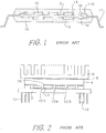
- the present invention relates to a three-dimensional multi-chip module comprising a plurality of semiconductor chips, and more particularly to the structure of a multi-chip module which achieves a higher integration density and a high power output.
- FIG. 1 A plurality of semiconductor elements (chips) 10 are arranged on both surfaces of a substrate 2. Wiring patterns and electrode terminals (not shown) are formed in advance on the surfaces of the substrate 2, and bonding pads formed on each semiconductor element 10 are operatively connected to electrode terminals of the wiring patterns by bonding wires 13.
- the substrate 2 with semiconductor elements 10 is disposed on a stage 11a of a lead frame 11, and electrode terminals of the wiring pattern are operatively connected by boding wires 15 to inner leads 11b of the lead frame 11.
- boding wires 15 to inner leads 11b of the lead frame 11.
- a wireless bonding method In order to obtain a higher integration density in a multi-chip module, a wireless bonding method has been utilized.
- a flip-chip method As the wireless bonding method, a flip-chip method, a beam lead method and a TAB (tape automated bonding) method are widely known.
- the flip-chip method is most effective for saving bonding area on the surface of a substrate.
- FIG. 2 shows an example of a multi-chip module of the prior art, in which the multi-chip module comprises two high output power semiconductor elements 10a.
- the multi-chip module further comprises two semiconductor elements 10b heat dissipation of which is comparatively small.
- All semiconductor elements 10a, 10b are bonded facedown to a substrate 2 by the flip-chip bonding method, namely, bumps 14 of solder are formed in advance on the major surface of the semiconductor elements and the semiconductor elements are disposed on the substrate 2, thereby the bumps on the major surface being brought in contact with electrode terminals of wiring pattern (not shown) on the substrate 2 and bonded together, and the wiring pattern being connected to outer leads 12.
- the back surface of the high power semiconductor elements 10a is further made in contact with a heat conductive base 4 using heat conductive paste 16 therebetween. After fixing a heat sink 5 to the above package, the multi-chip module is finally completed.
- the package structure of the prior art of Figure 2 encloses semiconductor elements which are arranged two-dimensionally on a front surface of the substrate 2 only. Therefore, an integration density can not be increased to the level of three-dimensional multi-chip module. Further, there is a problem that mixed disposition of the semiconductor elements is difficult, in which one semiconductor element requires wire bonding and the other semiconductor element requires flip-chip bonding.
- a three-dimensional multi-chip module of the present invention comprising: a substrate having a first and second surface, and comprising wiring patterns having a plurality of electrode terminals on the first and second surfaces respectively, at least a single semiconductor element arranged facedown on the first surface of the substrate and operatively connected to the electrode terminals on the first surface, at least a single semiconductor element and/or passive element arranged on the second surface of the substrate and operatively connected to the electrode terminals on the second surface, and a heat conductive base facing the first surface of the substrate and thermally in contact with the back surface of the semiconductor element arranged on the first surface of the substrate.
- the multi-chip module of the present invention further comprises a support base and a cap, forming an enclosure together with the heat conductive base, and a heat sink fixed to the heat conductive base, which results in achieving a high integration density and a high power of the module.
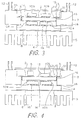
- Figure 3 shows a schematic cross section of an embodiment of a three-dimensional multi-chip module in accordance with the present invention.
- a support base 3, a heat conductive base 4 and a cap 7 form a packaging enclosure of the multi-chip module, and a substrate 2 with semiconductor elements 10a, 10b is enclosed therein.
- a heat sink 5 is attached to the heat conductive base 4 and enhances heat handling capability of the multi-chip module.
- the substrate 2 is made of multilayer ceramic and predetermined wiring patterns are formed between ceramic layers and/or on the surface of the substrate by the known technology.
- a plurality of semiconductor elements 10a, 10b are arranged on a first and second surface of the substrate 2, thereby the first surface being defined for the surface which subsequently faces the heat conductive base 4 after packaging.
- the semiconductor element 10a which requires comparatively large heat dissipation is arranged on the first surface of the substrate 2, and the semiconductor element 10b which requires comparatively small heat dissipation is arranged on the second surface thereof. Therefore, a semiconductor element which dissipates several watts to tens of watts is preferably arranged on the first surface of the substrate 2.
- both semiconductor elements 10a, 10b are bonded facedown to the first and second surfaces of the substrate 2, namely, the major surface comprising main integrated circuits of the semiconductor element is bonded facing the substrate 2.
- a flip-chip method is applied for bonding the semiconductor elements 10a, 10b and, in this case, a plurality of bumps 14 which are to be bonded to electrode terminals of the wiring pattern, are formed in advance on the major surface of the semiconductor elements.
- the semiconductor elements 10a, 10b are disposed at the predetermined positions respectively on the first and second surfaces of the substrate 2 and they are heated for reflowing the solder of the bumps.
- a subassembly composed of the semiconductor elements 10a, 10b and the substrate 2 is mounted on another subassembly composed of the support base 3 and the heat conductive base 4, thereby these two parts being fixed together by thermal conductive resin or solder.
- the support base 3 is made of multilayer ceramic and comprises a buried wiring pattern (not shown) and a plurality of outer leads 12 and a plurality of electrode terminals 31. The outer leads 12 and electrode terminals 31 are operatively connected by the wiring pattern.
- the material used for the heat conductive base 4 is required to have a high thermal conductivity and also have a thermal expansion coefficient which is close to that of silicon as much as possible.
- Porous sintered copper-tungsten (Cu-W) and sintered copper-molybdenum (Cu-Mo) have a thermal expansion coefficient of approx. 6x10 ⁇ 6/deg, and these materials are favorable as the heat conductive base 4 on which silicon chip (having a thermal expansion coefficient of about 2.6x10 ⁇ 6/deg) is disposed.
- the substrate 2 with semiconductor elements 10a, 10b is mounted on the heat conductive base 4 in a manner that the minor surfaces (back surfaces) of the semiconductor elements 10a are fixed to the heat conductive base 4 using heat conductive adhesive 16 such as Ag paste, solder, etc. between the thermal conductive base 4 and the minor surface of the semiconductor elements 10a, and further the substrate 2 is fixed to the support base 3 using insulating thermal conductive resin therebetween.
- heat conductive adhesive 16 such as Ag paste, solder, etc.
- electrode terminals 31 on the step portion of the support base 3 and electrode terminals 21 on the substrate 2 are connected by bonding wires 15.
- a heat sink 5 of aluminum or aluminum alloy is fixed on the outer surface of the heat conductive base 4 using thermal compound, and the cap 7 of iron-nickel alloy closes an opening of the support base 3.
- Figure 4 shows a schematic cross section of another embodiment of a three-dimensional multi-chip module of the present invention.
- Semiconductor elements 10a having comparatively a large heat dissipation are arranged facedown on the first surface (bottom surface) of the substrate 2 and bonded thereto in the same way as in Figure 3.
- semiconductor elements 10b having comparatively a small heat dissipation are arranged faceup on the second surface (front surface) of the substrate 2, and pads (not shown) on the semiconductor element 10b are connected to electrode terminals on the substrate 2 using a bonding wire 13.
- a passive elements 6 such as capacitor, coil, and resistor are arranged on the second surface of the substrate 2 and connected to the electrode terminals on the substrate 2.
- Figure 4 shows that active and/or passive elements which require a wire-bonding method can be mixed and comprised in the module using the second surface of the substrate 2.
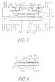
- Figure 5 shows a schematic cross section of still another embodiment of the present invention.
- the module of Figure 5 further comprises a heat conductive metal member 9 having elasticity.
- One end 9a of the metal member 9 is fixed to an inside surface of the cap 7.
- the other end 9b of the metal member 9 is elastically in contact with the inside surface of the cap 7 and can move when the metal member 9 is subjected to thermal expansion.
- the middle portion of the metal member 9 is elastically in contact with the second surface of the substrate 2 and pressing the second surface of the substrate 2 when the cap 7 closes the opening of the support base 3.
- semiconductor elements 10b and/or passive elements 6 arranged on the second surface of the substrate 2 have no direct heat removing means such as the heat conductive base 4 for the semiconductor elements 10a on the first surface of the substrate 2, heats generated in semiconductor elements 10b and passive elements 6 are conducted to the substrate 2. Temperature rise of the substrate 2 can be remarkably reduced by the function of the above metal member 9 by conducting the heat of the substrate 2 to the cap 7 which is cooled by the ambient atmosphere.
- the shape of the metal member 9 in Figure 5 shows an illustrative one, and many other shapes can be used.
- One end of the metal member 9 may be fixed to the substrate 2 and the other end may be in contact with the cap 7 or vice versa, thereby metal member 9 having a "U" character shape being used laying its side up.
- Figure 6 shows a schematic cross section of a modified structure of a substrate 2 with semiconductor elements 10a, 10b arranged thereon.
- Wiring patterns (not shown) on the substrate 2 has test terminals 22 other than electrode terminals 21 which are actually used for bonding the semiconductor elements 10a, 10b and subsequently for connecting the wiring patterns to the outside electrode terminals.
- the subassembly of Figure 6 comprising the substrate 2 and the semiconductor elements 10a, 10b bonded thereto, is subjected to function test, in which the entire circuit of the module is divided into several circuit blocks and each circuit block is tested using the test terminals 22 and/or electrode terminals 21.
- the substrate 2 with semiconductor elements 10a, 10b is packaged in the enclosure of support base 3, heat conductive base 4 and cap 7.
- all semiconductor elements 10a, 10b are bonded facedown to the substrate 2 using bumps 14.
- a substrate 2 having test terminals 22 can be utilized for other multi-chip module comprising semiconductor elements requiring wire bonding and/or passive elements.
Abstract
A three-dimensional multi-chip module having a high integration density and a high power output in accordance with the present invention comprising:
a substrate (2) having wiring patterns with a plurality of electrode terminals (21), at least a single semiconductor element (10a) arranged facedown on the bottom surface of the substrate (2) and operatively connected to the electrode terminals (21), at least a single semiconductor element (10b) and/or passive element (6) arranged on the front surface of the substrate (2) and operatively connected to the electrode terminals (21), a heat conductive base (4) facing the bottom surface of the substrate (2) and thermally in contact with the back surface of the semiconductor element (2) arranged on the bottom surface of the substrate (2), a support base (3), a cap (7) and a heat sink (5), thereby the heat conductive base (4), the support base (3) and the cap (7) forming an enclosure of the substrate (2).
a substrate (2) having wiring patterns with a plurality of electrode terminals (21), at least a single semiconductor element (10a) arranged facedown on the bottom surface of the substrate (2) and operatively connected to the electrode terminals (21), at least a single semiconductor element (10b) and/or passive element (6) arranged on the front surface of the substrate (2) and operatively connected to the electrode terminals (21), a heat conductive base (4) facing the bottom surface of the substrate (2) and thermally in contact with the back surface of the semiconductor element (2) arranged on the bottom surface of the substrate (2), a support base (3), a cap (7) and a heat sink (5), thereby the heat conductive base (4), the support base (3) and the cap (7) forming an enclosure of the substrate (2).
Description
- The present invention relates to a three-dimensional multi-chip module comprising a plurality of semiconductor chips, and more particularly to the structure of a multi-chip module which achieves a higher integration density and a high power output.
- The most typical three-dimensional multi-chip module of the prior art is schematically illustrated in Figure 1. A plurality of semiconductor elements (chips) 10 are arranged on both surfaces of a
substrate 2. Wiring patterns and electrode terminals (not shown) are formed in advance on the surfaces of thesubstrate 2, and bonding pads formed on eachsemiconductor element 10 are operatively connected to electrode terminals of the wiring patterns bybonding wires 13. Thesubstrate 2 withsemiconductor elements 10 is disposed on astage 11a of a lead frame 11, and electrode terminals of the wiring pattern are operatively connected byboding wires 15 to inner leads 11b of the lead frame 11. Thus formed subassembly is molded in amold package 18 of epoxy resin. - In order to obtain a higher integration density in a multi-chip module, a wireless bonding method has been utilized. As the wireless bonding method, a flip-chip method, a beam lead method and a TAB (tape automated bonding) method are widely known. Among these methods, the flip-chip method is most effective for saving bonding area on the surface of a substrate.
- When the multi-chip module includes a semiconductor element which dissipates a lot of heat during operation, there arises another problem how to give off the heat generated in the semiconductor element out of the multi-chip module. Figure 2 shows an example of a multi-chip module of the prior art, in which the multi-chip module comprises two high output
power semiconductor elements 10a. The multi-chip module further comprises twosemiconductor elements 10b heat dissipation of which is comparatively small. Allsemiconductor elements substrate 2 by the flip-chip bonding method, namely,bumps 14 of solder are formed in advance on the major surface of the semiconductor elements and the semiconductor elements are disposed on thesubstrate 2, thereby the bumps on the major surface being brought in contact with electrode terminals of wiring pattern (not shown) on thesubstrate 2 and bonded together, and the wiring pattern being connected toouter leads 12. The back surface of the highpower semiconductor elements 10a is further made in contact with a heatconductive base 4 using heatconductive paste 16 therebetween. After fixing aheat sink 5 to the above package, the multi-chip module is finally completed. - The package structure of the prior art of Figure 2 encloses semiconductor elements which are arranged two-dimensionally on a front surface of the
substrate 2 only. Therefore, an integration density can not be increased to the level of three-dimensional multi-chip module. Further, there is a problem that mixed disposition of the semiconductor elements is difficult, in which one semiconductor element requires wire bonding and the other semiconductor element requires flip-chip bonding. - It is an object of the present invention to provide a multi-chip module having a high integration density and a high power output.
- It is another object of the present invention to provide a multi-chip module having a higher integration density and a high power output, in which high power semiconductor elements and low power semiconductor elements and/or passive elements are mixed and arranged three-dimensionally on both surfaces of a substrate.
- It is still another object of the present invention to provide a three-dimensional multi-chip module which comprises provision for directly removing the heat generated in high power semiconductor elements arranged on one side of a substrate.
- It is further object of the present invention to provide the three-dimensional multi-chip module which further comprises provision for indirectly cooling the elements arranged on the other side of the substrate by removing the heat of the substrate.
- The above objects are achieved by a three-dimensional multi-chip module of the present invention comprising: a substrate having a first and second surface, and comprising wiring patterns having a plurality of electrode terminals on the first and second surfaces respectively, at least a single semiconductor element arranged facedown on the first surface of the substrate and operatively connected to the electrode terminals on the first surface, at least a single semiconductor element and/or passive element arranged on the second surface of the substrate and operatively connected to the electrode terminals on the second surface, and a heat conductive base facing the first surface of the substrate and thermally in contact with the back surface of the semiconductor element arranged on the first surface of the substrate.
- The multi-chip module of the present invention further comprises a support base and a cap, forming an enclosure together with the heat conductive base, and a heat sink fixed to the heat conductive base, which results in achieving a high integration density and a high power of the module.
- Other and further objects and advantage of the invention will become more apparent from the following description, reference being had to the accompanied drawings.
-
- Figure 1 shows a schematic cross section of a multi-chip module of the prior art in which semiconductor elements are arranged on both surfaces of a substrate and packaged in a resin mold,
- Figure 2 shows a schematic cross section of a multi-chip module of the prior art in which semiconductor elements are arranged on a front surface of a substrate only and a heat sink is provided for cooling high power semiconductor elements,
- Figure 3 shows a schematic cross section of an embodiment of a three-dimensional multi-chip module of the present invention in which high power and low power semiconductor elements are respectively arranged on bottom and front surfaces of a substrate, and cooling provision are provided for the high power semiconductor elements,
- Figure 4 shows a schematic cross section of another embodiment of a three-dimensional multi-chip module of the present invention in which high power semiconductor elements are arranged on a bottom surface and low power semiconductor elements and/or a passive element are arranged on a front surfaces of a substrate,
- Figure 5 shows a schematic cross section of still another embodiment of a three-dimensional multi-chip module of the present invention in which provision for cooling a substrate is added to the structure of Figure 4, and
- Figure 6 is a schematic side view of a subassembly of the present invention including a substrate and semiconductor elements, wherein the subassembly can be subjected to a preliminary test before it is packaged.
- Throughout the drawings, the same reference numerals designate and identify the same or similar parts.
- Figure 3 shows a schematic cross section of an embodiment of a three-dimensional multi-chip module in accordance with the present invention.
- A
support base 3, a heatconductive base 4 and acap 7 form a packaging enclosure of the multi-chip module, and asubstrate 2 withsemiconductor elements heat sink 5 is attached to the heatconductive base 4 and enhances heat handling capability of the multi-chip module. - The
substrate 2 is made of multilayer ceramic and predetermined wiring patterns are formed between ceramic layers and/or on the surface of the substrate by the known technology. A plurality ofsemiconductor elements substrate 2, thereby the first surface being defined for the surface which subsequently faces the heatconductive base 4 after packaging. Thesemiconductor element 10a which requires comparatively large heat dissipation is arranged on the first surface of thesubstrate 2, and thesemiconductor element 10b which requires comparatively small heat dissipation is arranged on the second surface thereof. Therefore, a semiconductor element which dissipates several watts to tens of watts is preferably arranged on the first surface of thesubstrate 2. - In Figure 3, both
semiconductor elements substrate 2, namely, the major surface comprising main integrated circuits of the semiconductor element is bonded facing thesubstrate 2. In Figure 3, a flip-chip method is applied for bonding thesemiconductor elements bumps 14 which are to be bonded to electrode terminals of the wiring pattern, are formed in advance on the major surface of the semiconductor elements. Thesemiconductor elements substrate 2 and they are heated for reflowing the solder of the bumps. - A subassembly composed of the
semiconductor elements substrate 2 is mounted on another subassembly composed of thesupport base 3 and the heatconductive base 4, thereby these two parts being fixed together by thermal conductive resin or solder. Thesupport base 3 is made of multilayer ceramic and comprises a buried wiring pattern (not shown) and a plurality ofouter leads 12 and a plurality ofelectrode terminals 31. Theouter leads 12 andelectrode terminals 31 are operatively connected by the wiring pattern. - The material used for the heat
conductive base 4 is required to have a high thermal conductivity and also have a thermal expansion coefficient which is close to that of silicon as much as possible. Porous sintered copper-tungsten (Cu-W) and sintered copper-molybdenum (Cu-Mo) have a thermal expansion coefficient of approx. 6x10⁻⁶/deg, and these materials are favorable as the heatconductive base 4 on which silicon chip (having a thermal expansion coefficient of about 2.6x10⁻⁶/deg) is disposed. - The
substrate 2 withsemiconductor elements conductive base 4 in a manner that the minor surfaces (back surfaces) of thesemiconductor elements 10a are fixed to the heatconductive base 4 using heatconductive adhesive 16 such as Ag paste, solder, etc. between the thermalconductive base 4 and the minor surface of thesemiconductor elements 10a, and further thesubstrate 2 is fixed to thesupport base 3 using insulating thermal conductive resin therebetween. - Next,
electrode terminals 31 on the step portion of thesupport base 3 andelectrode terminals 21 on thesubstrate 2 are connected bybonding wires 15. - Finally, a
heat sink 5 of aluminum or aluminum alloy is fixed on the outer surface of the heatconductive base 4 using thermal compound, and thecap 7 of iron-nickel alloy closes an opening of thesupport base 3. Thus, the three- dimensional multi-chip module of the embodiment is completed. - Figure 4 shows a schematic cross section of another embodiment of a three-dimensional multi-chip module of the present invention.
Semiconductor elements 10a having comparatively a large heat dissipation are arranged facedown on the first surface (bottom surface) of thesubstrate 2 and bonded thereto in the same way as in Figure 3. On the other hand,semiconductor elements 10b having comparatively a small heat dissipation are arranged faceup on the second surface (front surface) of thesubstrate 2, and pads (not shown) on thesemiconductor element 10b are connected to electrode terminals on thesubstrate 2 using abonding wire 13. Further apassive elements 6 such as capacitor, coil, and resistor are arranged on the second surface of thesubstrate 2 and connected to the electrode terminals on thesubstrate 2. - Figure 4 shows that active and/or passive elements which require a wire-bonding method can be mixed and comprised in the module using the second surface of the
substrate 2. - Figure 5 shows a schematic cross section of still another embodiment of the present invention. The only one difference in structure between Figure 4 and Figure 5 exists in that the module of Figure 5 further comprises a heat
conductive metal member 9 having elasticity. Oneend 9a of themetal member 9 is fixed to an inside surface of thecap 7. Theother end 9b of themetal member 9 is elastically in contact with the inside surface of thecap 7 and can move when themetal member 9 is subjected to thermal expansion. The middle portion of themetal member 9 is elastically in contact with the second surface of thesubstrate 2 and pressing the second surface of thesubstrate 2 when thecap 7 closes the opening of thesupport base 3. - Since
semiconductor elements 10b and/orpassive elements 6 arranged on the second surface of thesubstrate 2 have no direct heat removing means such as the heatconductive base 4 for thesemiconductor elements 10a on the first surface of thesubstrate 2, heats generated insemiconductor elements 10b andpassive elements 6 are conducted to thesubstrate 2. Temperature rise of thesubstrate 2 can be remarkably reduced by the function of theabove metal member 9 by conducting the heat of thesubstrate 2 to thecap 7 which is cooled by the ambient atmosphere. - The shape of the
metal member 9 in Figure 5 shows an illustrative one, and many other shapes can be used. One end of themetal member 9 may be fixed to thesubstrate 2 and the other end may be in contact with thecap 7 or vice versa, therebymetal member 9 having a "U" character shape being used laying its side up. - Figure 6 shows a schematic cross section of a modified structure of a
substrate 2 withsemiconductor elements substrate 2 hastest terminals 22 other thanelectrode terminals 21 which are actually used for bonding thesemiconductor elements substrate 2 having thesemiconductor elements substrate 2 and thesemiconductor elements test terminals 22 and/orelectrode terminals 21. - When any of the circuit blocks is found to be defective, a defective semiconductor element can be easily replaced with a good one. After confirming the subassembly works satisfactory, the
substrate 2 withsemiconductor elements support base 3, heatconductive base 4 andcap 7. In Figure 6, allsemiconductor elements substrate 2 using bumps 14. Asubstrate 2 havingtest terminals 22 can be utilized for other multi-chip module comprising semiconductor elements requiring wire bonding and/or passive elements. - The present invention may be embodied in other specific forms. The presently disclosed embodiments are, therefore, to be considered in all respects as illustrative and not restrictive, the scope of the invention being indicated by the appended claims, rather than the foregoing description, and all changes which come within the meaning and range of equivalence of the claims are, therefore, to be embraced therein.
Claims (11)
- A multi-chip module having a plurality of semiconductor elements arranged three-dimensionally, said multi-chip module comprising:
a substrate (2) having a first surface and a second surface, and wiring patterns including a plurality of electrode terminals (21) formed on the first and second surfaces respectively,
at least a single semiconductor element (10a) arranged facedown on the first surface of the substrate (2) and operatively connected to the electrode terminals (21) on the first surface,
at least a single semiconductor element (10b) arranged on the second surface of the substrate (2) and operatively connected to the electrode terminals (21) on the second surface, and
a heat conductive base (4) facing the first surface of the substrate and thermally in contact with a back surface of the semiconductor element (10a) arranged on the first surface of the substrate (2). - A multi-chip module as recited in claim 1, said multi-chip module further comprising:
a support base (3) having a plurality of outer leads (12) and a plurality of electrode terminals operatively connected to the outer leads (12) and having an opening for accepting said substrate (2) with the semiconductor elements (10a,10b) therein, thereby the electrode terminals on the support base (3) being operatively connected to said electrode terminals on the substrate (2) and an end surface of the support base (3) being fixed to the periphery of said heat conductive base (4). - A multi-chip module as recited in claim 2, said multi-chip module further comprising:
a cap (7) disposed on said support base (3) facing the second surface of the substrate (2), thereby said heat conductive base (4), said support base (3) and the cap (7) forming an enclosure inside which said substrate (2) is disposed. - A multi-chip module as recited in anyone of claims 1 to 3, said multi-chip module further comprising:
a heat sink (5) for cooling said heat conductive base (4). - A multi-chip module as recited in anyone of claims 1 to 4, wherein said semiconductor element (10a) on the first surface of the substrate (2) is the one whose heat dissipation is large and said semiconductor element (10b) on the second surface is the one whose heat dissipation is small.
- A multi-chip module as recited in anyone of claims 1 to 5, said multi-chip module further comprising:
a passive element (6) arranged on the second surface of the substrate (2). - A multi-chip module as recited in anyone of claims 1 to 6, wherein material of said heat conductive base (4) has a thermal expansion coefficient close to that of the semiconductor element (2).
- A multi-chip module as recited in anyone of claims 2 to 7, wherein said substrate (2) and said support base (3) are made of ceramic.
- A multi-chip module as recited in anyone of claims 3 to 8, said multi-chip module further comprising:
an elastic metal member (9) of heat conductive material inserted between the second surface of said substrate (2) and the inside surface of said cap (7). - A multi-chip module as recited in claim 9, wherein one and (9a) of said metal member (9) is fixed to the inside surface of the cap (7), the other end (9b) thereof is movable in contact with the inside surface of the cap (7), and the middle portion thereof is in contact with said second surface of the substrate (2).
- A multi-chip module as recited in anyone of claims 1 to 10, wherein said wiring pattern further comprises test terminals (22), whereby the test terminals (22) are used for testing each circuit block of a subassembly composed of said semiconductor elements (10a,10b) and the substrate (2) before packaging into the multi-chip module.
Applications Claiming Priority (2)
| Application Number | Priority Date | Filing Date | Title |
|---|---|---|---|
| JP3202089A JPH0548000A (en) | 1991-08-13 | 1991-08-13 | Semiconductor device |
| JP202089/91 | 1991-08-13 |
Publications (1)
| Publication Number | Publication Date |
|---|---|
| EP0528367A1 true EP0528367A1 (en) | 1993-02-24 |
Family
ID=16451786
Family Applications (1)
| Application Number | Title | Priority Date | Filing Date |
|---|---|---|---|
| EP92113849A Withdrawn EP0528367A1 (en) | 1991-08-13 | 1992-08-13 | Three-dimensional multi-chip module |
Country Status (4)
| Country | Link |
|---|---|
| US (1) | US5297006A (en) |
| EP (1) | EP0528367A1 (en) |
| JP (1) | JPH0548000A (en) |
| KR (1) | KR930005177A (en) |
Cited By (14)
| Publication number | Priority date | Publication date | Assignee | Title |
|---|---|---|---|---|
| EP0729652A1 (en) * | 1993-11-16 | 1996-09-04 | Formfactor, Inc. | Contact structure for interconnections, interposer, semiconductor assembly and method |
| EP0694968A3 (en) * | 1994-07-26 | 1996-09-11 | Nec Corp | Multi-chip module semiconductor device |
| EP0792517A1 (en) * | 1994-11-15 | 1997-09-03 | Formfactor, Inc. | Electrical contact structures from flexible wire |
| US6049976A (en) | 1993-11-16 | 2000-04-18 | Formfactor, Inc. | Method of mounting free-standing resilient electrical contact structures to electronic components |
| EP0996155A2 (en) * | 1998-10-23 | 2000-04-26 | Sony Corporation | Radio frequency integrated circuit apparatus |
| US6336269B1 (en) | 1993-11-16 | 2002-01-08 | Benjamin N. Eldridge | Method of fabricating an interconnection element |
| US6727579B1 (en) | 1994-11-16 | 2004-04-27 | Formfactor, Inc. | Electrical contact structures formed by configuring a flexible wire to have a springable shape and overcoating the wire with at least one layer of a resilient conductive material, methods of mounting the contact structures to electronic components, and applications for employing the contact structures |
| WO2004061861A2 (en) * | 2002-12-31 | 2004-07-22 | Matrix Semiconductor, Inc. | Nand memory array incorporating capacitance boosting of channel regions in unselected memory cells and method for operation of same |
| US6778406B2 (en) | 1993-11-16 | 2004-08-17 | Formfactor, Inc. | Resilient contact structures for interconnecting electronic devices |
| US7005350B2 (en) | 2002-12-31 | 2006-02-28 | Matrix Semiconductor, Inc. | Method for fabricating programmable memory array structures incorporating series-connected transistor strings |
| US7023739B2 (en) | 2003-12-05 | 2006-04-04 | Matrix Semiconductor, Inc. | NAND memory array incorporating multiple write pulse programming of individual memory cells and method for operation of same |
| US7221588B2 (en) | 2003-12-05 | 2007-05-22 | Sandisk 3D Llc | Memory array incorporating memory cells arranged in NAND strings |
| US8485418B2 (en) | 1995-05-26 | 2013-07-16 | Formfactor, Inc. | Method of wirebonding that utilizes a gas flow within a capillary from which a wire is played out |
| CN112420636A (en) * | 2020-11-19 | 2021-02-26 | 四川长虹空调有限公司 | Chip heat radiation structure |
Families Citing this family (55)
| Publication number | Priority date | Publication date | Assignee | Title |
|---|---|---|---|---|
| JPH0786717A (en) * | 1993-09-17 | 1995-03-31 | Fujitsu Ltd | Printing wiring board structure |
| US5772451A (en) * | 1993-11-16 | 1998-06-30 | Form Factor, Inc. | Sockets for electronic components and methods of connecting to electronic components |
| JPH07202463A (en) * | 1994-01-11 | 1995-08-04 | Yokogawa Electric Corp | Electronic circuit module |
| AT402135B (en) * | 1994-03-30 | 1997-02-25 | Electrovac | CIRCUIT BOARD |
| CN1037134C (en) * | 1994-07-04 | 1998-01-21 | 松下电器产业株式会社 | Integrated circuit device |
| EP0693776B1 (en) * | 1994-07-15 | 2000-05-31 | Mitsubishi Materials Corporation | Highly heat-radiating ceramic package |
| JPH0846136A (en) * | 1994-07-26 | 1996-02-16 | Fujitsu Ltd | Semiconductor device |
| US6031723A (en) * | 1994-08-18 | 2000-02-29 | Allen-Bradley Company, Llc | Insulated surface mount circuit board construction |
| JP2636777B2 (en) * | 1995-02-14 | 1997-07-30 | 日本電気株式会社 | Semiconductor module for microprocessor |
| SE515416C2 (en) * | 1995-02-16 | 2001-07-30 | Ericsson Telefon Ab L M | Device for integrated circuits, and method for its assembly |
| TW373308B (en) * | 1995-02-24 | 1999-11-01 | Agere Systems Inc | Thin packaging of multi-chip modules with enhanced thermal/power management |
| US5572405A (en) * | 1995-06-07 | 1996-11-05 | International Business Machines Corporation (Ibm) | Thermally enhanced ball grid array package |
| US5607538A (en) * | 1995-09-07 | 1997-03-04 | Ford Motor Company | Method of manufacturing a circuit assembly |
| US6008988A (en) * | 1995-12-20 | 1999-12-28 | Intel Corporation | Integrated circuit package with a heat spreader coupled to a pair of electrical devices |
| US5785535A (en) * | 1996-01-17 | 1998-07-28 | International Business Machines Corporation | Computer system with surface mount socket |
| US5729052A (en) * | 1996-06-20 | 1998-03-17 | International Business Machines Corporation | Integrated ULSI heatsink |
| US5847927A (en) * | 1997-01-27 | 1998-12-08 | Raytheon Company | Electronic assembly with porous heat exchanger and orifice plate |
| US6188874B1 (en) | 1997-06-27 | 2001-02-13 | Lockheed Martin Corporation | Control and telemetry signal communication system for geostationary satellites |
| US5990418A (en) * | 1997-07-29 | 1999-11-23 | International Business Machines Corporation | Hermetic CBGA/CCGA structure with thermal paste cooling |
| US6019166A (en) * | 1997-12-30 | 2000-02-01 | Intel Corporation | Pickup chuck with an integral heatsink |
| US5990549A (en) * | 1998-02-06 | 1999-11-23 | Intel Corporation | Thermal bus bar design for an electronic cartridge |
| US6552264B2 (en) | 1998-03-11 | 2003-04-22 | International Business Machines Corporation | High performance chip packaging and method |
| US6369444B1 (en) * | 1998-05-19 | 2002-04-09 | Agere Systems Guardian Corp. | Packaging silicon on silicon multichip modules |
| US6265771B1 (en) | 1999-01-27 | 2001-07-24 | International Business Machines Corporation | Dual chip with heat sink |
| SE516139C2 (en) * | 1999-03-17 | 2001-11-26 | Ericsson Telefon Ab L M | Method and apparatus for improving the thermal and electrical properties of components connected to a substrate mounted on a carrier |
| US6890798B2 (en) | 1999-06-08 | 2005-05-10 | Intel Corporation | Stacked chip packaging |
| DE19928733A1 (en) * | 1999-06-23 | 2001-01-04 | Giesecke & Devrient Gmbh | Semiconductor memory chip module |
| US6297551B1 (en) * | 1999-09-22 | 2001-10-02 | Agere Systems Guardian Corp. | Integrated circuit packages with improved EMI characteristics |
| US6473310B1 (en) * | 2000-02-18 | 2002-10-29 | Stmicroelectronics S.R.L. | Insulated power multichip package |
| KR100890534B1 (en) * | 2000-02-25 | 2009-03-27 | 이비덴 가부시키가이샤 | Multilayer printed wiring board and method for producing multilayer printed wiring board |
| KR101093471B1 (en) | 2000-09-25 | 2011-12-13 | 이비덴 가부시키가이샤 | Semiconductor element, method of manufacturing semiconductor element, multi-layer printed circuit board, and method of manufacturing multi-layer printed circuit board |
| US6627980B2 (en) | 2001-04-12 | 2003-09-30 | Formfactor, Inc. | Stacked semiconductor device assembly with microelectronic spring contacts |
| US20050136640A1 (en) * | 2002-01-07 | 2005-06-23 | Chuan Hu | Die exhibiting an effective coefficient of thermal expansion equivalent to a substrate mounted thereon, and processes of making same |
| US6841413B2 (en) * | 2002-01-07 | 2005-01-11 | Intel Corporation | Thinned die integrated circuit package |
| TW577153B (en) * | 2002-12-31 | 2004-02-21 | Advanced Semiconductor Eng | Cavity-down MCM package |
| US6711021B1 (en) * | 2003-01-15 | 2004-03-23 | Hewlett-Packard Development Company, L.P. | Systems and methods that use at least one component to remove the heat generated by at least one other component |
| GB0304438D0 (en) * | 2003-02-27 | 2003-04-02 | Lang Andrew | Bicycle display and storage bracket |
| US7365273B2 (en) * | 2004-12-03 | 2008-04-29 | Delphi Technologies, Inc. | Thermal management of surface-mount circuit devices |
| US7310036B2 (en) * | 2005-01-10 | 2007-12-18 | International Business Machines Corporation | Heat sink for integrated circuit devices |
| US7473579B2 (en) * | 2005-01-31 | 2009-01-06 | Purdue Research Foundation | Self-aligned wafer level integration system |
| DE102005053974B3 (en) * | 2005-11-11 | 2007-03-01 | Siemens Ag | Electrical circuit arrangement has heat sink thermally coupled to a circuit carrier for electronic components and a second carrier within the first having an electronic component between it and the heat sink |
| US8174114B2 (en) * | 2005-12-15 | 2012-05-08 | Taiwan Semiconductor Manufacturing Go. Ltd. | Semiconductor package structure with constraint stiffener for cleaning and underfilling efficiency |
| JP4821537B2 (en) * | 2006-09-26 | 2011-11-24 | 株式会社デンソー | Electronic control unit |
| KR101489325B1 (en) * | 2007-03-12 | 2015-02-06 | 페어차일드코리아반도체 주식회사 | Power module with stacked flip-chip and method of fabricating the same power module |
| US20090080163A1 (en) * | 2007-05-17 | 2009-03-26 | Lockheed Martin Corporation | Printed wiring board assembly |
| US20100314730A1 (en) * | 2009-06-16 | 2010-12-16 | Broadcom Corporation | Stacked hybrid interposer through silicon via (TSV) package |
| US8680670B2 (en) | 2010-10-22 | 2014-03-25 | International Business Machines Corporation | Multi-chip module system with removable socketed modules |
| CN102891116B (en) | 2011-07-20 | 2015-06-10 | 讯芯电子科技(中山)有限公司 | Embedded element packaging structure and manufacturing method thereof |
| US20130119529A1 (en) * | 2011-11-15 | 2013-05-16 | Taiwan Semiconductor Manufacturing Company, Ltd. | Semiconductor device having lid structure and method of making same |
| US20130277855A1 (en) * | 2012-04-24 | 2013-10-24 | Terry (Teckgyu) Kang | High density 3d package |
| KR102127335B1 (en) * | 2012-10-29 | 2020-06-30 | 삼성전자주식회사 | Semiconductor Module |
| ITUB20153344A1 (en) * | 2015-09-02 | 2017-03-02 | St Microelectronics Srl | ELECTRONIC POWER MODULE WITH IMPROVED THERMAL DISSIPATION AND ITS MANUFACTURING METHOD |
| RU2656030C2 (en) * | 2016-07-14 | 2018-05-30 | Акционерное общество "Концерн радиостроения "Вега" | Method of manufacturing three-dimensional electronic module |
| DE102018201842A1 (en) * | 2018-02-06 | 2019-08-08 | Siemens Aktiengesellschaft | Power electronic circuit with multiple power modules |
| US11521939B2 (en) * | 2020-07-24 | 2022-12-06 | Advanced Semiconductor Engineering, Inc. | Semiconductor device structure having stiffener with two or more contact points for heat dissipating element |
Citations (2)
| Publication number | Priority date | Publication date | Assignee | Title |
|---|---|---|---|---|
| EP0264469A1 (en) * | 1986-10-21 | 1988-04-27 | International Business Machines Corporation | Package density doubling device for semiconductor chips containing monolithically integrated circuits |
| FR2630859A1 (en) * | 1988-04-27 | 1989-11-03 | Thomson Composants Militaires | Multilayer ceramic package with plural integrated-circuit microchips |
Family Cites Families (2)
| Publication number | Priority date | Publication date | Assignee | Title |
|---|---|---|---|---|
| FR2550009B1 (en) * | 1983-07-29 | 1986-01-24 | Inf Milit Spatiale Aeronaut | ELECTRONIC COMPONENT HOUSING PROVIDED WITH A CAPACITOR |
| JPS629649A (en) * | 1985-07-08 | 1987-01-17 | Nec Corp | Package for semiconductor |
-
1991
- 1991-08-13 JP JP3202089A patent/JPH0548000A/en not_active Withdrawn
-
1992
- 1992-07-21 US US07/916,264 patent/US5297006A/en not_active Expired - Fee Related
- 1992-08-10 KR KR1019920014319A patent/KR930005177A/en not_active Application Discontinuation
- 1992-08-13 EP EP92113849A patent/EP0528367A1/en not_active Withdrawn
Patent Citations (2)
| Publication number | Priority date | Publication date | Assignee | Title |
|---|---|---|---|---|
| EP0264469A1 (en) * | 1986-10-21 | 1988-04-27 | International Business Machines Corporation | Package density doubling device for semiconductor chips containing monolithically integrated circuits |
| FR2630859A1 (en) * | 1988-04-27 | 1989-11-03 | Thomson Composants Militaires | Multilayer ceramic package with plural integrated-circuit microchips |
Non-Patent Citations (1)
| Title |
|---|
| IBM TECHNICAL DISCLOSURE BULLETIN vol. 27, no. 7B, December 1984, NEW YORK page 4226 R.A.CICONE ET AL 'silicon integrated high performance package' * |
Cited By (28)
| Publication number | Priority date | Publication date | Assignee | Title |
|---|---|---|---|---|
| US6279227B1 (en) | 1993-11-16 | 2001-08-28 | Igor Y. Khandros | Method of forming a resilient contact structure |
| US7225538B2 (en) | 1993-11-16 | 2007-06-05 | Formfactor, Inc. | Resilient contact structures formed and then attached to a substrate |
| US6242803B1 (en) | 1993-11-16 | 2001-06-05 | Formfactor, Inc. | Semiconductor devices with integral contact structures |
| US6274823B1 (en) | 1993-11-16 | 2001-08-14 | Formfactor, Inc. | Interconnection substrates with resilient contact structures on both sides |
| EP0729652A4 (en) * | 1993-11-16 | 1998-06-24 | Formfactor Inc | Contact structure for interconnections, interposer, semiconductor assembly and method |
| US5900738A (en) * | 1993-11-16 | 1999-05-04 | Formfactor, Inc. | Contact structure device for interconnections, interposer, semiconductor assembly and package using the same and method |
| US5917707A (en) * | 1993-11-16 | 1999-06-29 | Formfactor, Inc. | Flexible contact structure with an electrically conductive shell |
| US5926951A (en) * | 1993-11-16 | 1999-07-27 | Formfactor, Inc. | Method of stacking electronic components |
| US6049976A (en) | 1993-11-16 | 2000-04-18 | Formfactor, Inc. | Method of mounting free-standing resilient electrical contact structures to electronic components |
| US6835898B2 (en) | 1993-11-16 | 2004-12-28 | Formfactor, Inc. | Electrical contact structures formed by configuring a flexible wire to have a springable shape and overcoating the wire with at least one layer of a resilient conductive material, methods of mounting the contact structures to electronic components, and applications for employing the contact structures |
| US6184587B1 (en) | 1993-11-16 | 2001-02-06 | Formfactor, Inc. | Resilient contact structures, electronic interconnection component, and method of mounting resilient contact structures to electronic components |
| US6778406B2 (en) | 1993-11-16 | 2004-08-17 | Formfactor, Inc. | Resilient contact structures for interconnecting electronic devices |
| EP0729652A1 (en) * | 1993-11-16 | 1996-09-04 | Formfactor, Inc. | Contact structure for interconnections, interposer, semiconductor assembly and method |
| US6476333B1 (en) | 1993-11-16 | 2002-11-05 | Formfactor, Inc. | Raised contact structures (solder columns) |
| US6336269B1 (en) | 1993-11-16 | 2002-01-08 | Benjamin N. Eldridge | Method of fabricating an interconnection element |
| EP0694968A3 (en) * | 1994-07-26 | 1996-09-11 | Nec Corp | Multi-chip module semiconductor device |
| EP0792517A1 (en) * | 1994-11-15 | 1997-09-03 | Formfactor, Inc. | Electrical contact structures from flexible wire |
| EP0792517A4 (en) * | 1994-11-15 | 1998-06-24 | Formfactor Inc | Electrical contact structures from flexible wire |
| US6727579B1 (en) | 1994-11-16 | 2004-04-27 | Formfactor, Inc. | Electrical contact structures formed by configuring a flexible wire to have a springable shape and overcoating the wire with at least one layer of a resilient conductive material, methods of mounting the contact structures to electronic components, and applications for employing the contact structures |
| US8485418B2 (en) | 1995-05-26 | 2013-07-16 | Formfactor, Inc. | Method of wirebonding that utilizes a gas flow within a capillary from which a wire is played out |
| EP0996155A2 (en) * | 1998-10-23 | 2000-04-26 | Sony Corporation | Radio frequency integrated circuit apparatus |
| EP0996155A3 (en) * | 1998-10-23 | 2001-04-18 | Sony Corporation | Radio frequency integrated circuit apparatus |
| US7005350B2 (en) | 2002-12-31 | 2006-02-28 | Matrix Semiconductor, Inc. | Method for fabricating programmable memory array structures incorporating series-connected transistor strings |
| WO2004061861A3 (en) * | 2002-12-31 | 2004-10-28 | Matrix Semiconductor Inc | Nand memory array incorporating capacitance boosting of channel regions in unselected memory cells and method for operation of same |
| WO2004061861A2 (en) * | 2002-12-31 | 2004-07-22 | Matrix Semiconductor, Inc. | Nand memory array incorporating capacitance boosting of channel regions in unselected memory cells and method for operation of same |
| US7023739B2 (en) | 2003-12-05 | 2006-04-04 | Matrix Semiconductor, Inc. | NAND memory array incorporating multiple write pulse programming of individual memory cells and method for operation of same |
| US7221588B2 (en) | 2003-12-05 | 2007-05-22 | Sandisk 3D Llc | Memory array incorporating memory cells arranged in NAND strings |
| CN112420636A (en) * | 2020-11-19 | 2021-02-26 | 四川长虹空调有限公司 | Chip heat radiation structure |
Also Published As
| Publication number | Publication date |
|---|---|
| US5297006A (en) | 1994-03-22 |
| JPH0548000A (en) | 1993-02-26 |
| KR930005177A (en) | 1993-03-23 |
Similar Documents
| Publication | Publication Date | Title |
|---|---|---|
| EP0528367A1 (en) | Three-dimensional multi-chip module | |
| US7208819B2 (en) | Power module package having improved heat dissipating capability | |
| US6380615B1 (en) | Chip size stack package, memory module having the same, and method of fabricating the module | |
| US7122401B2 (en) | Area array type semiconductor package fabrication method | |
| US6060768A (en) | Semiconductor device, method of manufacturing the semiconductor device, and method of manufacturing lead frame | |
| US6707140B1 (en) | Arrayable, scaleable, and stackable molded package configuration | |
| KR100393448B1 (en) | Semiconductor package and method for manufacturing the same | |
| KR0178623B1 (en) | Semiconductor device | |
| JPH0677357A (en) | Improved semiconductor package, improved method for packaging of integrated circuit device and method for cooling of semiconductor device | |
| KR20030018642A (en) | Stack chip module | |
| EP0645816B1 (en) | Semiconductor device comprising a plurality of semiconductor elements | |
| US20020079570A1 (en) | Semiconductor package with heat dissipating element | |
| US5757068A (en) | Carrier film with peripheral slits | |
| US6166435A (en) | Flip-chip ball grid array package with a heat slug | |
| US6075281A (en) | Modified lead finger for wire bonding | |
| CN113540056A (en) | Semiconductor module and method for manufacturing the same | |
| JPH0855875A (en) | Semiconductor device | |
| US5982026A (en) | Inexpensive resin molded semiconductor device | |
| CA2017080C (en) | Semiconductor device package structure | |
| KR100206880B1 (en) | Culumn type package, having heatsink | |
| US6318622B1 (en) | High power hybrid modules assembly using vacuum oven for permanent electrical connections | |
| US6538303B1 (en) | Lead frame and semiconductor device using the same | |
| JP2690248B2 (en) | Surface mount type semiconductor device | |
| JP2822990B2 (en) | CSP type semiconductor device | |
| JP2800806B2 (en) | Semiconductor device and manufacturing method thereof |
Legal Events
| Date | Code | Title | Description |
|---|---|---|---|
| PUAI | Public reference made under article 153(3) epc to a published international application that has entered the european phase |
Free format text: ORIGINAL CODE: 0009012 |
|
| AK | Designated contracting states |
Kind code of ref document: A1 Designated state(s): DE FR GB |
|
| 17P | Request for examination filed |
Effective date: 19930421 |
|
| 17Q | First examination report despatched |
Effective date: 19941202 |
|
| STAA | Information on the status of an ep patent application or granted ep patent |
Free format text: STATUS: THE APPLICATION IS DEEMED TO BE WITHDRAWN |
|
| 18D | Application deemed to be withdrawn |
Effective date: 19970301 |