EP0444601A2 - Memory access control - Google Patents
Memory access control Download PDFInfo
- Publication number
- EP0444601A2 EP0444601A2 EP91102810A EP91102810A EP0444601A2 EP 0444601 A2 EP0444601 A2 EP 0444601A2 EP 91102810 A EP91102810 A EP 91102810A EP 91102810 A EP91102810 A EP 91102810A EP 0444601 A2 EP0444601 A2 EP 0444601A2
- Authority
- EP
- European Patent Office
- Prior art keywords
- memory
- address
- data
- dram
- external memory
- Prior art date
- Legal status (The legal status is an assumption and is not a legal conclusion. Google has not performed a legal analysis and makes no representation as to the accuracy of the status listed.)
- Granted
Links
Images


Classifications
-
- G—PHYSICS
- G06—COMPUTING; CALCULATING OR COUNTING
- G06F—ELECTRIC DIGITAL DATA PROCESSING
- G06F12/00—Accessing, addressing or allocating within memory systems or architectures
- G06F12/02—Addressing or allocation; Relocation
- G06F12/06—Addressing a physical block of locations, e.g. base addressing, module addressing, memory dedication
- G06F12/0607—Interleaved addressing
Definitions
- the present invention relates to a data processor, and more specifically to a method of locating and controlling a memory device provided in the data processor.
- a typical conventional data processor includes a central processing unit (CPU) for executing data processing.
- the CPU is coupled to an address bus used to supply an address to an external device and a data bus for transferring data between the CPU and the external device.
- the CPU is coupled to a control bus used for controlling the external device.
- On typical CPU is adapted to handle a memory space in such a manner that a plurality of consecutive memory areas are treated as a one block.
- a width of an internal data bus is larger than a width of an external data bus. Therefore, a plurality of external bus cycles can be generated in response to one internal bus cycle.
- This type of CPU can be exemplified by Intel's microprocessor i8088 and a CPU including a cache controller therein.
- the cache controller has adopted a data exchange manner in which a memory space is divided into a plurality of blocks, and data exchange or transfer between a cache memory and an external memory is collectively executed in units of blocks.
- the data bus is coupled to a plurality of DRAMs (dynamic random access memory), which constitute external memories for the CPU.
- DRAMs dynamic random access memory
- Each of the DRAMs is controlled by one corresponding DRAM controller coupled to the address bus.
- Each DRAM controller is controlled by a control logic which is coupled to the CPU through a control bus in order to interface an operating timing between the control bus and the external device such as the DRAMs and the DRAM controller.
- the control logic supplies a common memory read signal and a common memory write signal to all the DRAM controllers.
- the DRAM controllers are also controlled by a decoder coupled to the address bus so that one of the DRAM controllers is selectively activated in response to a chip select signal generated by the decoder on the basis of the result of decoding of an address on the address bus.
- the DRAM is configured to be capable of executing a high speed page mode operation, in which if a row address does not change, a data exchange can be executed by changing only a column address and activating a column address strobe again.
- a row address and a column address are applied to the DRAM by executing an address input by two times. Therefore, since the input of the row address is unnecessary, the data exchange can be correspondingly executed at a high speed
- the DRAM has one restriction in which once a row address strobe is activated, a precharge period in which the row address strobe is made an inactive is required. If the precharge period is not satisfied, a content of the DRAM will be broken.
- the address bus is composed of 32 bits, and two 1M DRAMs are used, an address of 0000 0000 h to 000F FFFF h is assigned to a first DRAM, and an address of 0010 0000 h to 001F FFFF h is assigned to a second DRAM, in a memory map of the data processor.
- the suffix "h” means a hexadecimal notation.
- the CPU can access to the external device with units of block each of which includes a plurality of units of processing, similarly to the type including the cache memory therein.
- the units of processing is called a "word". For example one block includes four words.
- an operation of the conventional data processor will be discussed.
- an address is supplied to the address bus, and decoded by the decoder. If the supplied address designates the first DRAM, the decoder outputs an active chip select signal to a first DRAM controller associated with the first DRAM.
- an memory access is outputted to the control bus and converted by the control logic into an active memory read signal or into an active memory write signal. Now, assume that the memory read signal has been activated.
- the first DRAM controller associated with the first DRAM is activated.
- the row address strobe supplied to the first DRAM is activated by the first DRAM controller and thereafter maintained in an active condition.
- the first DRAM controller supplies an address signal to the first DRAM during a high level period of the T1 clock.
- the column address strobe supplied to the first DRAM is activated, so that a content of the first DRAM is outputted to the data bus.
- the data exchange is completed, and a first TB clock following the T2 clock rises.
- the TB clock is used in the high speed page mode operation, and makes it possible to execute the data exchange with only one clock.
- the column address strobe supplied to the first DRAM is inactivated, and a next address is supplied to the first DRAM during a high level period of the TB clock.
- the column address strobe supplied to the first DRAM is activated, and the a second data exchange is executed during a low level period of the TB clock.
- second and third clocks are generated so that the same memory reading operation (the data exchange) is executed three times. As a result, the data exchange is executed four times in total by the T1 and T2 clocks and the succeeding first to third TB clocks.
- a second bus cycle starts, and a T1 clock of the second bus cycle rises at an end of the low level period of the third TB clock of the first bus cycle.
- a next address is supplied to the address bus so that a memory access will be started.
- the row column strobe supplied to the first DRAM is inactivated, and maintained in an inactive condition for a period corresponding to one clock period, since a period for the precharging is required to have one clock period.
- the row column strobe supplied to the first DRAM is activated at a falling of the T2 clock of the second bus cycle.
- the staring of the memory access in the second bus cycle is delayed from the starting of the memory access in the first bus cycle by a period of time corresponding to one clock. Because of this, a TW clock is inserted between the T2 clock and the first TB clock in the second bus cycle, so that the CPU is brought into a wait condition so as to adjust the timing. This adjustment is controlled by the control logic.
- the DRAM has rapid access mode such as the high speed page mode which is higher than the ordinary access operations.
- ROMs read only memory
- SRAMs static random access memory
- ROMs or SRAMs are used, these memory resources are often located at the outside of the cache coverage.
- T1, T2, TB, TB and TB clocks the data exchange between the ROM or SRAM and the CPU is executed in a normal access mode (four sets of T1 and T2 clocks).
- the ROMs or SRAMs are located at the outside of the cache coverage, the performance of the data processor inevitably lowers. If the CPU operates in different modes, the control circuit becomes complicated.
- Another object of the present invention is to provide a data processor capable of continuously accessing the same region of an external device with the same period of time as that required when a different region is accessed.
- Still another object of the present invention is to provide a data processor capable of accessing a low access speed external device apparently as quick as the data processor accesses a high access speed external device.
- a data processor comprising a CPU and a memory accessed by the CPU, the memory being divided into a plurality of memory banks in such a manner that a size of one block that can be accessed by the CPU is assigned to one memory bank, the CPU generating a control signal for locating the memory banks in an interlaced or interleaved manner, one of the memory bank including a plurality of memory sub-banks, and the CPU generating another control signal for sequentially executing a data exchange between the CPU and the memory sub-banks.
- FIG. 1 there is shown a block diagram of a first embodiment of the data processor in accordance with the present invention.
- the shown data processor includes a central processing unit (CPU) 1 for executing data processing.
- the CPU is coupled to an address bus 2 used to supply an address to an external device and a data bus 2 for transferring data between the CPU and the external device.
- the address bus 2 has a width of 32 bits, and respective bits of the address bus are designated by A0, A1, . . . , A31, where the suffix added to the letter "A" shows a bit position.
- the CPU has a width of an internal data bus which is larger than a width of an external data bus. Therefore, a plurality of external bus cycles can be generated in response to one internal bus cycle.
- this type of CPU can be exemplified by Intel's microprocessor i8088 and a CPU including a cache controller therein.
- the data bus 3 is coupled to a plurality of DRAMs 8-1 DRAM0 and 8-2 DRAM1, which constitute external memories for the CPU.
- DRAM0 8-1 and DRAM1 8-2 are controlled by DRAM controllers (DRAMC) 7-1 and 7-2 coupled to the address bus 2.
- DRAM controllers (DRAMC) 7-1 and 7-2 are controlled by DRAM controllers (DRAMC) 7-1 and 7-2 coupled to the address bus 2.
- DRAM controller 7-1 and 7-2 is controlled by a control logic 5 which is coupled to the CPU through a control bus bus 4 in order to interface an operating timing between the control bus 4 and the external device such as the DRAMs and the DRAM controller.
- the control logic 5 supplies a common memory read signal MRD 9 and a common memory write signal MWR 10 to all the DRAM controllers 7-1 and 7-2 in parallel.
- the DRAM controllers are also controlled by an address decoder 6 coupled to the address bus 2.
- the address decoder 6 decodes a portion of an address on the address bus 2 and generates chip select signals MEM0CS and MOM1CS , which are supplied to a chip selection input CS of the DRAM controllers 7-1 and 7-2, respectively.
- the chip select signals MEM0CS and MOM1CS are an active low signal in which the signal is active when it is of "0" and inactive when it is of "1".
- an upper bar means an active low signal.
- the control logic 5 receives a bus cycle request from the CPU 1 through the control bus 4, and activate the memory read signal MRD 9 if the memory read is requested, and the memory write signal MWR 10 if the memory write is requested. In addition, when the memory (the external device to the CPU) completes the data exchange, the control logic 5 notifies it to the CPU 1 through the control bus 4.
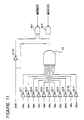
- the address decoder 5 is constituted of inverters 12-1 to 12-12, 11-input AND gate 13 and 2-input NAND gates 14-1 and 14-2, connected as shown in Figure 11.
- Address inputs DA0 to DA10 are respectively supplied through the inverters 12-1 to 12-11 to the AND gate 13, whose output is connected to the NAND gates 14-1 and 14-2.
- a Bank input BNK is supplied through the inverter 12-12 to the NAND gate 14-1 and directly to the NAND gate 14-2.
- the DRAM controllers 7-1 and 7-2 have the same construction, and therefore, inputs and outputs are shown only for the DRAM controller 7-1.
- a chip select input CS When a chip select input CS is active and when either the memory read signal MRD 9 or the memory write signal MWR 10 is active, the DRAM controller operates to control the associated DRAM.
- the DRAM controller has address inputs RA0 to RA19, and operates to supply the address inputs RA10 to RA19 (often called a "row address”) to address outputs MA0 to MA9, coupled to an address input port of the associated DRAM.
- the DRAM controller activates the row address strobe RAS .
- the DRAM controller activates a write enable signal WE .
- the DRAM controller operates to supply the address inputs RA0 to RA9 (often called a "column address”) to the address outputs MA0 to MA9 and at the same time, activates the column address strobe CAS .
- Each of the DRAMs 8-1 and 8-2 is configured to be capable of executing the high speed page mode operation as already explained hereinbefore
- the BNK input of the address decoder 6 is connected to the address bit A2 of the address bus 2
- the address inputs DA0 to DA10 of the address decoder 6 are connected to the address bits A21 to A31.
- the address inputs RA0 to RA19 of each DRAM controller are connected to the address bits A0, A1, A3 to A20.
- the BNK input of the address decoder 6 is connected to the address bit A20 of the address bus 2, and the address inputs RA0 to RA19 of each DRAM controller are connected to the address bits A0 to A19.
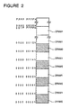
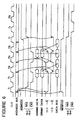
- FIG. 2 there is shown a memory map realized in accordance with the above mentioned connection between the address bus and the address decoder and the DRAM controllers.
- address 00000000 h to 00000003 h , 00000008 h to 0000000B h , 00000010 h to 00000013 h , 00000018 h to 0000001B h , . . . are assigned to the DRAM0 7-1.
- address 00000004 h to 00000007 h , 0000000C h to 0000000F h , 00000014 h to 00000017 h , 0000001C h to 0000001F h , . . . are assigned to the DRAM1 7-2.
- the memory banks are located by units of 4 words in the interleaved manner, differently from the conventional data processor in which, for example, memory banks are continuously located as shown in Figure 12.
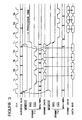
- FIG. 3 there is shown a timing chart illustrating the operation of the data processor shown in Figure 1.
- the address decoder 6 decode the address "0" and activates the chip select signal MEM0CS .
- the DRAM controller 7-1 activates the row address strobe RAS at a falling the T1 clock, so that access to the DRAM 8-1 starts. Thereafter, the row address strobe RAS is maintained in the active condition.
- the DRAM controller 7-1 supplies an address signal of MA0 to MA9 to the DRAM 8-1 during a high level period of the T1 clock.
- the column address strobe CAS supplied to the DRAM 7-1 is activated, so that a data exchanged between the DRAM 7-1 and the CPU 1 is executed through the data bus 3.
- the data exchange is completed, and a first TB clock following the T2 clock rises.
- the column address strobe CAS supplied to the DRAM 8-1 is inactivated, and a next address of MA0 to MA9 is supplied to the DRAM 8-1 during a high level period of the TB clock.
- the column address strobe CAS supplied to the DRAM 8-1 is activated, and the a second data exchange is executed during a low level period of the TB clock. Succeeding to the first TB clock, second and third clocks are generated so that the same memory reading operation (the data exchange) is executed three times. As a result, the data exchange is executed four times in total by the T1 and T2 clocks and the succeeding first to third TB clocks.
- data is read from or written to the addresses of 00000000 h to 00000003 h in the memory map shown in Figure 2.
- the memory access is alternately executed to the DRAM0 8-1 and the DRAM1 8-2, so that the delay of the access time caused for the precharging will not occur.
- the above mentioned embodiment is such that, in the memory space, memory blocks each composed of four words are located in the interleaved manner.
- the CPU under consideration can access four words as one block.
- the BNK input of the address decoder 6 is connected to the address bit A4 of the address bus 2
- the address inputs DA0 to DA10 of the address decoder 6 are connected to the address bits A21 to A31.
- the address inputs RA0 to RA19 of each DRAM controller are connected to the address bits A0, A1, A2, A3, A5, to A20.
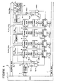
- FIG. 4 there is shown a second embodiment.
- This second embodiment is adapted to adjust a mismatching of the operating timing with the TB clocks, which is the second problem of the prior art discussed hereinbefore.
- the second embodiment includes inverters 15-1 to 15-4, two-input NAND gates 16-1 to 16-4, bidirectional buffers 17-1 to 17-4 having a latch function.
- the buffer When an input E is active, the buffer is open.
- DRAM controllers 18-1 to 18-4 are associated to the DRAMs 8-1 to 8-4.
- These DRAM controllers 18-1 to 18-4 operates basically similarly to conventional DRAM controller and the DRAM controller shown in Figure 1. However, the DRAM controllers 18-1 to 18-4 have a different high speed page mode, an operating timing of which will be explained hereinafter.
- the BNK input of the address decoder 6 is connected to the address bit A2 of the address bus 2, and the address inputs DA0 to DA9 of the address decoder 6 are connected to the address bits A22 to A31.
- the address input DA10 of the address decoder 6 is grounded.
- the address inputs RA0 to RA19 of each of the DRAM controllers 18-1 to 18-4 are connected to the address bits A1 and A3 to A20.
- the E input of the buffer 17-1 is connected to receive an output of the NAND gate 16-1 receiving an output of the inverter 15-2 receiving the MEM0CS signal and an output of the inverter 15-1 receiving the address bit A0.
- the E input of the buffer 17-2 is connected to receive an output of the NAND gate 16-2 receiving the address bit A0 and the output of the inverter 15-2.
- the E input of the buffer 17-3 is connected to receive an output of the NAND gate 16-3 receiving an output of the inverter 15-3 receiving the MOM1CS signal and an output of the inverter 15-4 receiving the address bit A0.
- the E input of the buffer 17-4 is connected to receive an output of the NAND gate 16-4 receiving the address bit A0 and the output of the inverter 15-3.
- the D input of each of the buffers 17-1 to 17-4 are connected to receive the memory write signal 10.
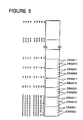
- FIG. 5 there is shown a memory map realized in the second embodiment.
- addresses of 00000000 h , 00000002 h , 00000008 h , 0000000A h , . . . are assigned to the DRAM00 8-1.
- Addresses of 00000001 h , 00000003 h , 00000009 h , 0000000B h , . . . are assigned to the DRAM01 8-2.
- Addresses of 00000004 h , 00000006 h , 0000000C h , 0000000E h , . . . are assigned to the DRAM10 8-3.
- Addresses of 00000005 h , 00000007 h , 0000000D h , 0000000F h , . . . are assigned to the DRAM11 8-4.
- FIG. 6 there is shown a timing chart illustrating the operation of the second embodiment of the data processor shown in Figure 4.
- the address on the address bus changes at a T1 clock in a first cycle. If the address decoder 6 activates the chip select signal MEM0CS . In response to this signal, the DRAM controllers 18-1 and 18-2 activate the row address strobe RAS , so that access to the DRAM00 8-1 and DRAM01 8-2 starts. Thereafter, at a rising of a T2 clock following the T1 clock, the column address strobe CAS of the DRAM controllers 18-1 and 18-2 is activated, so that a data exchange between the DRAM00 8-1 and the DRAM01 8-2 and the CPU 1 becomes possible. At this time, the E input of the buffer 17-1 is activated, a data exchange between the DRAM00 8-1 and the CPU 1 is executed.
- the address changes, with the result that the E input of the buffer 17-2 is activated, a data exchange between the DRAM01 8-2 and the CPU 1 is executed.
- the column address strobe CAS is inactivated.
- the column address strobe CAS is activated, again.
- the second embodiment After an end of the third TB clock, and at a T1 clock of a second cycle, the address changes, the chip select signal MEM0CS is inactivated and the chip select signal MOM1CS is activated. Therefore, the second embodiment can ensure the precharging time, similarly to the first embodiment.
- the transition timing of the column address strobe CAS from the active condition to the inactive condition and vice versa is expanded to one clock, while the transition timing is a half clock in the first embodiment. Therefore, the controlling timing of the DRAMs can be loosen.
- the memory includes eight banks.
- the third embodiment includes selectors 22-1 and 22-2. An operation of each selector is illustrated in the truth table shown in Figure 8.
- DRAM controllers 19-1 to 19-8 will be explained hereinafter when an operating timing is explained. These DRAM controllers 19-1 to 19-8 are associated to eight DRAMs 20-1 to 20-8 (DRAM00 to DRAM03 and DRAM01 to DRAM13). Buffers 21-1 to 21-8 have the same function as the buffer 17 shown in Figure 4.
- the BNK input of the address decoder 6 is connected to the address bit A2 of the address bus 2, and the address inputs DA0 to DA8 of the address decoder 6 are connected to the address bits A23 to A31.
- the address inputs DA9 and DA10 of the address decoder 6 is grounded.
- the address inputs of each DRAM controller are connected to the address bits A3 to A20.
- the A and B inputs of each selector are connected to the address bits A0 and A1.
- the G input of the selector 18-1 is connected to receive the MEM0CS signal
- the G input of the selector 18-2 is connected to receive the MOM1CS signal.
- addresses of 00000000 h , 00000008 h , . . . are assigned to the DRAM00. Addresses of 00000001 h , 00000009 h , . . . are assigned to the DRAM01. Addresses of 00000002 h , 0000000A h , . . . are assigned to the DRAM02. Addresses of 00000003 h , 0000000B h , . . . are assigned to the DRAM03. Addresses of 00000004 h , 0000000C h , . . . are assigned to the DRAM10.
- Addresses of 00000005 h , 0000000D h , . . . are assigned to the DRAM11. Addresses of 00000006 h , 0000000E h , . . . are assigned to the DRAM12. Addresses of 00000007 h , 0000000F h , . . . are assigned to the DRAM13.
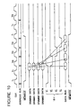
- FIG. 10 there is shown a timing chart illustrating the operation of the third embodiment of the data processor shown in Figure 7.
- the address decoder 6 activates the chip select signal MEM0CS .
- the DRAM controllers 19-1 to 19-4 activate the row address strobe RAS , so that access to the DRAM00 to DRAM03 starts.
- the Y0 output of the selector 22-1 is activated, so that a data exchange between the DRAM00 and the CPU 1 is executed at an end of the T2 clock, namely at a rising of a first TB clock.
- the Y1 output of the selector 22-1 is activated, so that a data exchange between the DRAM01 and the CPU 1 is executed.
- the Y2 output of the selector 22-1 is activated at the second TB clock, so that a data exchange between the DRAM10 and the CPU 1 is executed.
- the Y3 output of the selector 22-1 is activated at the third TB clock, so that a data exchange between the DRAM11 and the CPU 1 is executed.
- the DRAMs since the four DRAMs (DRAM00 to DRAM03 or DRAM10 to DRAM13) are driven at the same one-time timing, the DRAM high speed page mode access is not used. Therefore, the DRAMs and the DRAM controllers can be replaced by memories such as ROMs or SRAMs which have a constant access speed.
Abstract
Description
- The present invention relates to a data processor, and more specifically to a method of locating and controlling a memory device provided in the data processor.
- A typical conventional data processor includes a central processing unit (CPU) for executing data processing. The CPU is coupled to an address bus used to supply an address to an external device and a data bus for transferring data between the CPU and the external device. In addition, the CPU is coupled to a control bus used for controlling the external device. On typical CPU is adapted to handle a memory space in such a manner that a plurality of consecutive memory areas are treated as a one block. In this CPU, a width of an internal data bus is larger than a width of an external data bus. Therefore, a plurality of external bus cycles can be generated in response to one internal bus cycle. This type of CPU can be exemplified by Intel's microprocessor i8088 and a CPU including a cache controller therein. As known, the cache controller has adopted a data exchange manner in which a memory space is divided into a plurality of blocks, and data exchange or transfer between a cache memory and an external memory is collectively executed in units of blocks.
- In addition, the data bus is coupled to a plurality of DRAMs (dynamic random access memory), which constitute external memories for the CPU. Each of the DRAMs is controlled by one corresponding DRAM controller coupled to the address bus. Each DRAM controller is controlled by a control logic which is coupled to the CPU through a control bus in order to interface an operating timing between the control bus and the external device such as the DRAMs and the DRAM controller. Typically, the control logic supplies a common memory read signal and a common memory write signal to all the DRAM controllers. The DRAM controllers are also controlled by a decoder coupled to the address bus so that one of the DRAM controllers is selectively activated in response to a chip select signal generated by the decoder on the basis of the result of decoding of an address on the address bus.
- The DRAM is configured to be capable of executing a high speed page mode operation, in which if a row address does not change, a data exchange can be executed by changing only a column address and activating a column address strobe again. In a normal access mode, a row address and a column address are applied to the DRAM by executing an address input by two times. Therefore, since the input of the row address is unnecessary, the data exchange can be correspondingly executed at a high speed
On the other hand, the DRAM has one restriction in which once a row address strobe is activated, a precharge period in which the row address strobe is made an inactive is required. If the precharge period is not satisfied, a content of the DRAM will be broken. - Now, assuming that the address bus is composed of 32 bits, and two 1M DRAMs are used, an address of 0000 0000h to 000F FFFFh is assigned to a first DRAM, and an address of 0010 0000h to 001F FFFFh is assigned to a second DRAM, in a memory map of the data processor. Here, the suffix "h" means a hexadecimal notation. In addition, the CPU can access to the external device with units of block each of which includes a plurality of units of processing, similarly to the type including the cache memory therein. Here, the units of processing is called a "word". For example one block includes four words.
- Under the above mentioned conditions, an operation of the conventional data processor will be discussed. At a T1 clock of a first bus cycle, an address is supplied to the address bus, and decoded by the decoder. If the supplied address designates the first DRAM, the decoder outputs an active chip select signal to a first DRAM controller associated with the first DRAM. On the other hand, an memory access is outputted to the control bus and converted by the control logic into an active memory read signal or into an active memory write signal. Now, assume that the memory read signal has been activated.
- In response to the active chip select signal and the active memory read signal, the first DRAM controller associated with the first DRAM is activated. As result, at a falling of the T1 clock, the row address strobe supplied to the first DRAM is activated by the first DRAM controller and thereafter maintained in an active condition. Then, the first DRAM controller supplies an address signal to the first DRAM during a high level period of the T1 clock. At a rising of a T2 clock following the T1 clock, the column address strobe supplied to the first DRAM is activated, so that a content of the first DRAM is outputted to the data bus. At an end of a low level period of the T2 clock, the data exchange is completed, and a first TB clock following the T2 clock rises. The TB clock is used in the high speed page mode operation, and makes it possible to execute the data exchange with only one clock. At a rising of the first TB clock, the column address strobe supplied to the first DRAM is inactivated, and a next address is supplied to the first DRAM during a high level period of the TB clock. At a falling of the first TB clock, the column address strobe supplied to the first DRAM is activated, and the a second data exchange is executed during a low level period of the TB clock. Succeeding to the first TB clock, second and third clocks are generated so that the same memory reading operation (the data exchange) is executed three times. As a result, the data exchange is executed four times in total by the T1 and T2 clocks and the succeeding first to third TB clocks.
- Following the first bus cycle, a second bus cycle starts, and a T1 clock of the second bus cycle rises at an end of the low level period of the third TB clock of the first bus cycle. At the T1 clock, a next address is supplied to the address bus so that a memory access will be started. However, at a falling of the T1 clock of the second bus cycle, the row column strobe supplied to the first DRAM is inactivated, and maintained in an inactive condition for a period corresponding to one clock period, since a period for the precharging is required to have one clock period. As a result, the row column strobe supplied to the first DRAM is activated at a falling of the T2 clock of the second bus cycle. Namely, the staring of the memory access in the second bus cycle is delayed from the starting of the memory access in the first bus cycle by a period of time corresponding to one clock. Because of this, a TW clock is inserted between the T2 clock and the first TB clock in the second bus cycle, so that the CPU is brought into a wait condition so as to adjust the timing. This adjustment is controlled by the control logic.
- As seen from the above, when the same bank of the memory is continuously accessed by the CPU, the data exchange, which will be completed with five clocks in ordinary cases, requires six clocks. As a result, the processing capacity of the data processor will correspondingly decrease. If first and second accesses are made to different backs, respectively, a second access can be completed with five clocks. However, considering a processing situation of the CPU, an instruction reading operation is of course executed for consecutive memory backs, and data precessed by the CPU is collectively stored in some region of the memory (localization of access region). Therefore, possibility of access to the same bank is higher than possibility of access to different banks. As a result, opportunity of the six clock access is much.
- The above mentioned operation time was made on the basic of clocks. In fact, however, various operating timings of different DRAMs coupled to the CPU must be satisfied. For example, an access period of time from the activation of the column address strobe until the completion of the data exchange must be ensured. Therefore, if the processing capacity of the data processor is increased by increasing the frequency of the clock, the operation based on the T1 and T2 clocks can be adjusted by inserting the TW clock for waiting, bur it is not possible to adjust the operation of the TB clock by inserting the TW clock. As a result, there occurs a situation in which the operating timing (for example, the access period of time starting from the activation of the column address strobe) cannot be satisfied. In this situation, the data processor cannot properly operate.
- In addition, the DRAM has rapid access mode such as the high speed page mode which is higher than the ordinary access operations. However, ROMs (read only memory) and SRAMs (static random access memory) ceaselessly require the same access time. In the case that these memories are coupled to the CPU, if the CPU is adapted to execute a first memory access by the T1 and T2 clocks and each of succeeding memory accesses by one TB clock as in the conventional example explained hereinbefore, it is requires that the memory access can be completed by only one clock. As a result, expensive ROMs or SRAMs are required.
- Furthermore, if ROMs or SRAMs are used, these memory resources are often located at the outside of the cache coverage. In addition, it is necessary to generate various control signals so that the data exchange between the DRAM and the CPU is executed in the high speed access mode (T1, T2, TB, TB and TB clocks) and the data exchange between the ROM or SRAM and the CPU is executed in a normal access mode (four sets of T1 and T2 clocks). However, if the ROMs or SRAMs are located at the outside of the cache coverage, the performance of the data processor inevitably lowers. If the CPU operates in different modes, the control circuit becomes complicated.
- Accordingly, it is an object of the present invention to provide a data processor which has overcome the above mentioned defect of the conventional one.
- Another object of the present invention is to provide a data processor capable of continuously accessing the same region of an external device with the same period of time as that required when a different region is accessed.
- Still another object of the present invention is to provide a data processor capable of accessing a low access speed external device apparently as quick as the data processor accesses a high access speed external device.
- The above and other objects of the present invention are achieved in accordance with the present invention by a data processor comprising a CPU and a memory accessed by the CPU, the memory being divided into a plurality of memory banks in such a manner that a size of one block that can be accessed by the CPU is assigned to one memory bank, the CPU generating a control signal for locating the memory banks in an interlaced or interleaved manner, one of the memory bank including a plurality of memory sub-banks, and the CPU generating another control signal for sequentially executing a data exchange between the CPU and the memory sub-banks.
- The above and other objects, features and advantages of the present invention will be apparent from the following description of preferred embodiments of the invention with reference to the accompanying drawings.
-
- Figure 1 is a block diagram of a first embodiment of the data processor in accordance with the present invention;
- Figure 2 shows a memory map realized in the data processor shown in Figure 1;
- Figure 3 is a timing chart showing an operation of the data processor shown in Figure 1, in which two banks of memory are provided and a number of block each of which includes four words are located in the interleaved manner;
- Figure 4 is a block diagram of a second embodiment of the data processor in accordance with the present invention;
- Figure 5 shows a memory map realized in the data processor shown in Figure 4;
- Figure 6 is a timing chart showing an operation of the data processor shown in Figure 4, in which four banks of memory are provided and each of the memory banks includes two sub-banks;
- Figure 7 is a block diagram of a third embodiment of the data processor in accordance with the present invention;
- Figure 8 is a truth table illustrating an operation of the selector shown in Figure 7;
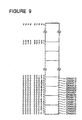
- Figure 9 shows a memory map realized in the data processor shown in Figure 7;
- Figure 10 is a timing chart showing an operation of the data processor shown in Figure 7, in which four banks of memory are provided and each of the memory banks includes four sub-banks;
- Figure 11 is a logic diagram of the address decoder shown in Figure 1; and
- Figure 12 shows a memory map realized in a typical conventional data processor.
- Referring to Figure 1, there is shown a block diagram of a first embodiment of the data processor in accordance with the present invention.
- The shown data processor includes a central processing unit (CPU) 1 for executing data processing. The CPU is coupled to an
address bus 2 used to supply an address to an external device and adata bus 2 for transferring data between the CPU and the external device. In the shown embodiment, theaddress bus 2 has a width of 32 bits, and respective bits of the address bus are designated by A₀, A₁, . . . , A₃₁, where the suffix added to the letter "A" shows a bit position. Here, the CPU has a width of an internal data bus which is larger than a width of an external data bus. Therefore, a plurality of external bus cycles can be generated in response to one internal bus cycle. As mentioned hereinbefore, this type of CPU can be exemplified by Intel's microprocessor i8088 and a CPU including a cache controller therein. - In addition, the
data bus 3 is coupled to a plurality of DRAMs 8-1 DRAM0 and 8-2 DRAM1, which constitute external memories for the CPU. DRAM0 8-1 and DRAM1 8-2 are controlled by DRAM controllers (DRAMC) 7-1 and 7-2 coupled to theaddress bus 2. Each of the DRAM controller 7-1 and 7-2 is controlled by acontrol logic 5 which is coupled to the CPU through acontrol bus bus 4 in order to interface an operating timing between thecontrol bus 4 and the external device such as the DRAMs and the DRAM controller. Thecontrol logic 5 supplies a common memory readsignal MRD 9 and a common memorywrite signal MWR 10 to all the DRAM controllers 7-1 and 7-2 in parallel. The DRAM controllers are also controlled by anaddress decoder 6 coupled to theaddress bus 2. Theaddress decoder 6 decodes a portion of an address on theaddress bus 2 and generates chip select signalsMEM0CS andMOM1CS , which are supplied to a chip selection inputCS of the DRAM controllers 7-1 and 7-2, respectively. Here, the chip select signalsMEM0CS andMOM1CS are an active low signal in which the signal is active when it is of "0" and inactive when it is of "1". In this specification, an upper bar means an active low signal. - The
control logic 5 receives a bus cycle request from theCPU 1 through thecontrol bus 4, and activate the memory readsignal MRD 9 if the memory read is requested, and the memorywrite signal MWR 10 if the memory write is requested. In addition, when the memory (the external device to the CPU) completes the data exchange, thecontrol logic 5 notifies it to theCPU 1 through thecontrol bus 4. - For example, the
address decoder 5 is constituted of inverters 12-1 to 12-12, 11-input ANDgate 13 and 2-input NAND gates 14-1 and 14-2, connected as shown in Figure 11. Address inputs DA₀ to DA₁₀ are respectively supplied through the inverters 12-1 to 12-11 to the ANDgate 13, whose output is connected to the NAND gates 14-1 and 14-2. A Bank input BNK is supplied through the inverter 12-12 to the NAND gate 14-1 and directly to the NAND gate 14-2. With this arrangement, if all of address inputs DA₀ to DA₁₀ are of "0" and the BNK input is also of "0", theNAND gate 14 1 activates the chip select signalMEM0CS . When all of address inputs DA₀ to DA₁₀ are of "0" and the BNK input is of "1", the NAND gate 14-2 activates the chip select signalMOM1CS . - The DRAM controllers 7-1 and 7-2 have the same construction, and therefore, inputs and outputs are shown only for the DRAM controller 7-1. When a chip select input
CS is active and when either the memory readsignal MRD 9 or the memorywrite signal MWR 10 is active, the DRAM controller operates to control the associated DRAM. The DRAM controller has address inputs RA₀ to RA₁₉, and operates to supply the address inputs RA₁₀ to RA₁₉ (often called a "row address") to address outputs MA₀ to MA₉, coupled to an address input port of the associated DRAM. At the same time, the DRAM controller activates the row address strobeRAS . At this time, if the memory write signal MWR is active, the DRAM controller activates a write enable signalWE . Thereafter, the DRAM controller operates to supply the address inputs RA₀ to RA₉ (often called a "column address") to the address outputs MA₀ to MA₉ and at the same time, activates the column address strobeCAS . - Each of the DRAMs 8-1 and 8-2 is configured to be capable of executing the high speed page mode operation as already explained hereinbefore
The above mentioned arrangement and construction are fundamentally the same as those of the conventional data processor. According to the present invention, the BNK input of theaddress decoder 6 is connected to the address bit A₂ of theaddress bus 2, and the address inputs DA₀ to DA₁₀ of theaddress decoder 6 are connected to the address bits A₂₁ to A₃₁. On the other hand, the address inputs RA₀ to RA₁₉ of each DRAM controller are connected to the address bits A₀, A₁, A₃ to A₂₀. (For reference, in a typical conventional data processor, the BNK input of theaddress decoder 6 is connected to the address bit A₂₀ of theaddress bus 2, and the address inputs RA₀ to RA₁₉ of each DRAM controller are connected to the address bits A₀ to A₁₉.) - Referring to Figure 2, there is shown a memory map realized in accordance with the above mentioned connection between the address bus and the address decoder and the DRAM controllers. As shown in Figure 2, address 00000000h to 00000003h, 00000008h to 0000000Bh, 00000010h to 00000013h, 00000018h to 0000001Bh, . . . are assigned to the DRAM0 7-1. On the other hand, address 00000004h to 00000007h, 0000000Ch to 0000000Fh, 00000014h to 00000017h, 0000001Ch to 0000001Fh, . . . are assigned to the DRAM1 7-2. Namely, the memory banks are located by units of 4 words in the interleaved manner, differently from the conventional data processor in which, for example, memory banks are continuously located as shown in Figure 12.
- Referring to Figure 3, there is shown a timing chart illustrating the operation of the data processor shown in Figure 1.
- Assume that the address "0" is outputted to the address bus at a T1 clock in a first cycle. The
address decoder 6 decode the address "0" and activates the chip select signalMEM0CS . In response to this signal, the DRAM controller 7-1 activates the row address strobeRAS at a falling the T1 clock, so that access to the DRAM 8-1 starts. Thereafter, the row address strobeRAS is maintained in the active condition. - Then, the DRAM controller 7-1 supplies an address signal of MA₀ to MA₉ to the DRAM 8-1 during a high level period of the T1 clock. At a rising of a T2 clock following the T1 clock, the column address strobe
CAS supplied to the DRAM 7-1 is activated, so that a data exchanged between the DRAM 7-1 and theCPU 1 is executed through thedata bus 3. At an end of a low level period of the T2 clock, the data exchange is completed, and a first TB clock following the T2 clock rises. At a rising of the first TB clock, the column address strobeCAS supplied to the DRAM 8-1 is inactivated, and a next address of MA₀ to MA₉ is supplied to the DRAM 8-1 during a high level period of the TB clock. At a falling of the first TB clock, the column address strobeCAS supplied to the DRAM 8-1 is activated, and the a second data exchange is executed during a low level period of the TB clock. Succeeding to the first TB clock, second and third clocks are generated so that the same memory reading operation (the data exchange) is executed three times. As a result, the data exchange is executed four times in total by the T1 and T2 clocks and the succeeding first to third TB clocks. Thus, data is read from or written to the addresses of 00000000h to 00000003h in the memory map shown in Figure 2. - Now, assume that an address of "4" is outputted to the
address bus 2 in a T1 clock of a second cycle succeeding to the first cycle. In this situation, the chip select signalMEM0CS is inactivated and the chip select signalMOM1CS is activated. As a result, the access to the DRAM1 8-2 is executed completely similarly to the above mentioned access to the DRAM0 8-1. At this time, the DRAM controller 7-1 inactivates the row address strobeRAS , so that the precharging period of time can be endure for the DRAM0 8-1. As a result, data is read from or written to the addresses of 00000004h to 00000007h in the memory map shown in Figure 2. - As seen from the above, although the data is read from or written to apparently continuous addresses in the memory, the memory access is alternately executed to the DRAM0 8-1 and the DRAM1 8-2, so that the delay of the access time caused for the precharging will not occur.
- The above mentioned embodiment is such that, in the memory space, memory blocks each composed of four words are located in the interleaved manner. The reason for this is that the CPU under consideration can access four words as one block. For example, if the CPU is adapted to access sixteen words as one block, memory blocks each composed of sixteen words are located in the interleaved manner. In this case, the BNK input of the
address decoder 6 is connected to the address bit A₄ of theaddress bus 2, and the address inputs DA₀ to DA₁₀ of theaddress decoder 6 are connected to the address bits A₂₁ to A₃₁. On the other hand, the address inputs RA₀ to RA₁₉ of each DRAM controller are connected to the address bits A₀, A₁, A₂, A₃, A₅, to A₂₀. - Referring to Figure 4, there is shown a second embodiment. This second embodiment is adapted to adjust a mismatching of the operating timing with the TB clocks, which is the second problem of the prior art discussed hereinbefore.
- In Figure 4, elements similar to those shown in Figure 1 are given the same Reference Numerals and explanation thereof will be omitted. In the second embodiment, four DRAMs 8-1 to 8-4 are provided, and each of these DRAM is similar to the DRAMs shown in Figure 1.
- The second embodiment includes inverters 15-1 to 15-4, two-input NAND gates 16-1 to 16-4, bidirectional buffers 17-1 to 17-4 having a latch function. When an input
E is active, the buffer is open. On the other hand, if an input D is of "1", data is supplied from thedata bus 3 to the DRAM, and when the input D is of "0", data is supplied from the DRAM to thedata bus 3
DRAM controllers 18-1 to 18-4 are associated to the DRAMs 8-1 to 8-4. These DRAM controllers 18-1 to 18-4 operates basically similarly to conventional DRAM controller and the DRAM controller shown in Figure 1. However, the DRAM controllers 18-1 to 18-4 have a different high speed page mode, an operating timing of which will be explained hereinafter. - The BNK input of the
address decoder 6 is connected to the address bit A₂ of theaddress bus 2, and the address inputs DA₀ to DA₉ of theaddress decoder 6 are connected to the address bits A₂₂ to A₃₁. The address input DA₁₀ of theaddress decoder 6 is grounded. On the other hand, the address inputs RA₀ to RA₁₉ of each of the DRAM controllers 18-1 to 18-4 are connected to the address bits A₁ and A₃ to A₂₀. - The
E input of the buffer 17-1 is connected to receive an output of the NAND gate 16-1 receiving an output of the inverter 15-2 receiving theMEM0CS signal and an output of the inverter 15-1 receiving the address bit A₀. TheE input of the buffer 17-2 is connected to receive an output of the NAND gate 16-2 receiving the address bit A₀ and the output of the inverter 15-2. TheE input of the buffer 17-3 is connected to receive an output of the NAND gate 16-3 receiving an output of the inverter 15-3 receiving theMOM1CS signal and an output of the inverter 15-4 receiving the address bit A₀. TheE input of the buffer 17-4 is connected to receive an output of the NAND gate 16-4 receiving the address bit A₀ and the output of the inverter 15-3. On the other hand, the D input of each of the buffers 17-1 to 17-4 are connected to receive thememory write signal 10. - Referring to Figure 5, there is shown a memory map realized in the second embodiment. As shown in Figure 5, addresses of 00000000h, 00000002h, 00000008h, 0000000Ah, . . . are assigned to the DRAM00 8-1. Addresses of 00000001h, 00000003h, 00000009h, 0000000Bh, . . . are assigned to the DRAM01 8-2. Addresses of 00000004h, 00000006h, 0000000Ch, 0000000Eh, . . . are assigned to the DRAM10 8-3. Addresses of 00000005h, 00000007h, 0000000Dh, 0000000Fh, . . . are assigned to the DRAM11 8-4.
- Referring to Figure 6, there is shown a timing chart illustrating the operation of the second embodiment of the data processor shown in Figure 4.
- The address on the address bus changes at a T1 clock in a first cycle. If the
address decoder 6 activates the chip select signalMEM0CS . In response to this signal, the DRAM controllers 18-1 and 18-2 activate the row address strobeRAS , so that access to the DRAM00 8-1 and DRAM01 8-2 starts. Thereafter, at a rising of a T2 clock following the T1 clock, the column address strobeCAS of the DRAM controllers 18-1 and 18-2 is activated, so that a data exchange between the DRAM00 8-1 and the DRAM01 8-2 and theCPU 1 becomes possible. At this time, theE input of the buffer 17-1 is activated, a data exchange between the DRAM00 8-1 and theCPU 1 is executed. At a first TB clock, the address changes, with the result that theE input of the buffer 17-2 is activated, a data exchange between the DRAM01 8-2 and theCPU 1 is executed. On the other hand, at a rising of the first TB clock, the column address strobeCAS is inactivated. At a rising of a second TB clock, the column address strobeCAS is activated, again. Thus, the DRAM10 and the DRAM11 sequentially execute the data exchange, similarly to the DRAM00 and the DRAM01. - After an end of the third TB clock, and at a T1 clock of a second cycle, the address changes, the chip select signal
MEM0CS is inactivated and the chip select signalMOM1CS is activated. Therefore, the second embodiment can ensure the precharging time, similarly to the first embodiment. - In the second embodiment, the transition timing of the column address strobe
CAS from the active condition to the inactive condition and vice versa is expanded to one clock, while the transition timing is a half clock in the first embodiment. Therefore, the controlling timing of the DRAMs can be loosen. - Referring to Figure 7, there is shown a third embodiment. In Figure 7, elements similar to those shown in Figures 1 and 4 are given the same Reference Numerals and explanation thereof will be omitted. In the third embodiment, the memory includes eight banks.
- The third embodiment includes selectors 22-1 and 22-2. An operation of each selector is illustrated in the truth table shown in Figure 8.
- When a
G input of each selector is inactive,Y₀ ,Y₁ ,Y₂ andY₃ outputs are inactive ("1"). When theG input is active, if A and B inputs are "0, 0",Y₀ is active, and if A and B inputs are "0, 1 ",Y₁ is active. If A and B inputs are "1, 0",Y₂ is active, and if A and B inputs are "1, 1",Y₃ is active. - DRAM controllers 19-1 to 19-8 will be explained hereinafter when an operating timing is explained. These DRAM controllers 19-1 to 19-8 are associated to eight DRAMs 20-1 to 20-8 (DRAM00 to DRAM03 and DRAM01 to DRAM13). Buffers 21-1 to 21-8 have the same function as the buffer 17 shown in Figure 4.
- The BNK input of the
address decoder 6 is connected to the address bit A₂ of theaddress bus 2, and the address inputs DA₀ to DA₈ of theaddress decoder 6 are connected to the address bits A₂₃ to A₃₁. The address inputs DA₉ and DA₁₀ of theaddress decoder 6 is grounded. On the other hand, the address inputs of each DRAM controller are connected to the address bits A₃ to A₂₀. In addition, the A and B inputs of each selector are connected to the address bits A₀ and A₁. TheG input of the selector 18-1 is connected to receive theMEM0CS signal, and theG input of the selector 18-2 is connected to receive theMOM1CS signal. - Referring to Figure 9, there is shown a memory map realized in the third embodiment. As shown in Figure 9, addresses of 00000000h, 00000008h, . . . are assigned to the DRAM00. Addresses of 00000001h, 00000009h, . . . are assigned to the DRAM01. Addresses of 00000002h, 0000000Ah, . . . are assigned to the DRAM02. Addresses of 00000003h, 0000000Bh, . . . are assigned to the DRAM03. Addresses of 00000004h, 0000000Ch, . . . are assigned to the DRAM10. Addresses of 00000005h, 0000000Dh, . . . are assigned to the DRAM11. Addresses of 00000006h, 0000000Eh, . . . are assigned to the DRAM12. Addresses of 00000007h, 0000000Fh, . . . are assigned to the DRAM13.
- Referring to Figure 10, there is shown a timing chart illustrating the operation of the third embodiment of the data processor shown in Figure 7.
- If the address on the address bus changes at a T1 clock in a first cycle, the
address decoder 6 activates the chip select signalMEM0CS . In response to this signal, the DRAM controllers 19-1 to 19-4 activate the row address strobeRAS , so that access to the DRAM00 to DRAM03 starts. In response to the address outputted in synchronism to the T1 clock, theY₀ output of the selector 22-1 is activated, so that a data exchange between the DRAM00 and theCPU 1 is executed at an end of the T2 clock, namely at a rising of a first TB clock. Similarly, at the first TB clock, theY₁ output of the selector 22-1 is activated, so that a data exchange between the DRAM01 and theCPU 1 is executed. TheY₂ output of the selector 22-1 is activated at the second TB clock, so that a data exchange between the DRAM10 and theCPU 1 is executed. TheY₃ output of the selector 22-1 is activated at the third TB clock, so that a data exchange between the DRAM11 and theCPU 1 is executed. - In the fourth embodiment, since the four DRAMs (DRAM00 to DRAM03 or DRAM10 to DRAM13) are driven at the same one-time timing, the DRAM high speed page mode access is not used. Therefore, the DRAMs and the DRAM controllers can be replaced by memories such as ROMs or SRAMs which have a constant access speed.
- The invention has thus been shown and described with reference to the specific embodiments. However, it should be noted that the present invention is in no way limited to the details of the illustrated structures but changes and modifications may be made within the scope of the appended claims.
Claims (2)
- A data processor which includes a central processing unit coupled to an address bus for supplying an address to an external memory and a data bus for supplying data to the external memory and receiving data from the external memory, and control means for controlling data exchange between the central processing unit and the external memory with a predetermined unit amount of data processing of the central processing unit, wherein the improvement comprises a plurality of memory circuits having the same structure and constituting the external memory, means for alternately assigning to the plurality of memory circuits a plurality of consecutive units obtained by dividing the predetermined unit amount of data processing of the central processing unit, and means for sequentially assigning a memory access from the central processing unit to the plurality of consecutive units.
- A data processor which includes a central processing unit coupled to an address bus for supplying an address to an external memory and a data bus for supplying data to the external memory and receiving data from the external memory, and a control means for controlling data exchange between the central processing unit and the external memory with a predetermined unit amount of data processing of the central processing unit, wherein the external memory includes first and second memory circuits and the central processing unit executes the data exchange with units of four word, each memory circuits having a memory area divided into a number of sub-areas each have four continuous addresses, so that the sub-areas of the first memory circuit and the sub-area of the second memory circuit are alternately assigned in continuous addresses in one memory space formed of the first and second memory circuits, and when an continuous addresses are supplied, the first and second memory circuits are alternately accessed by a controller means.
Applications Claiming Priority (3)
| Application Number | Priority Date | Filing Date | Title |
|---|---|---|---|
| JP2046089A JPH03248243A (en) | 1990-02-26 | 1990-02-26 | Information processor |
| JP4608990 | 1990-02-26 | ||
| JP46089/90 | 1990-02-26 |
Publications (3)
| Publication Number | Publication Date |
|---|---|
| EP0444601A2 true EP0444601A2 (en) | 1991-09-04 |
| EP0444601A3 EP0444601A3 (en) | 1992-01-22 |
| EP0444601B1 EP0444601B1 (en) | 1999-10-27 |
Family
ID=12737262
Family Applications (1)
| Application Number | Title | Priority Date | Filing Date |
|---|---|---|---|
| EP91102810A Expired - Lifetime EP0444601B1 (en) | 1990-02-26 | 1991-02-26 | Data processor with interleaved DRAM memory |
Country Status (4)
| Country | Link |
|---|---|
| US (1) | US5274788A (en) |
| EP (1) | EP0444601B1 (en) |
| JP (1) | JPH03248243A (en) |
| DE (1) | DE69131734T2 (en) |
Cited By (6)
| Publication number | Priority date | Publication date | Assignee | Title |
|---|---|---|---|---|
| EP0657807A1 (en) * | 1993-12-09 | 1995-06-14 | International Business Machines Corporation | Method and system for efficient instruction execution in a data processing system having multiple prefetch units |
| WO2000067129A1 (en) * | 1999-04-30 | 2000-11-09 | Matsushita Electric Industrial Co., Ltd. | Memory control unit |
| WO2004006103A1 (en) * | 2002-07-09 | 2004-01-15 | Globespanvirata Incorporated | Method and system for improving access latency of multiple bank devices |
| US6810449B1 (en) | 1995-10-19 | 2004-10-26 | Rambus, Inc. | Protocol for communication with dynamic memory |
| US6931467B2 (en) | 1995-10-19 | 2005-08-16 | Rambus Inc. | Memory integrated circuit device which samples data upon detection of a strobe signal |
| US7562184B2 (en) * | 2004-01-07 | 2009-07-14 | Panasonic Corporation | DRAM controller for graphics processing operable to enable/disable burst transfer |
Families Citing this family (28)
| Publication number | Priority date | Publication date | Assignee | Title |
|---|---|---|---|---|
| ATE179810T1 (en) * | 1991-03-01 | 1999-05-15 | Advanced Micro Devices Inc | MICROPROCESSOR WITH EXTERNAL MEMORY |
| IT1244938B (en) * | 1991-03-06 | 1994-09-13 | Ezio Lefons | DATA INTERROGATION SYSTEM IN THE DATABASES AND DATABASES. |
| JPH04293135A (en) * | 1991-03-20 | 1992-10-16 | Yokogawa Hewlett Packard Ltd | Memory access system |
| CA2116985C (en) * | 1993-03-11 | 1999-09-21 | Cynthia J. Burns | Memory system |
| US5410664A (en) * | 1993-03-31 | 1995-04-25 | Intel Corporation | RAM addressing apparatus with lower power consumption and less noise generation |
| JPH0713859A (en) * | 1993-06-25 | 1995-01-17 | Mitsubishi Electric Corp | Controller for semiconductor storage element |
| US5848258A (en) * | 1994-06-30 | 1998-12-08 | Digital Equipment Corporation | Memory bank addressing scheme |
| JPH0822444A (en) * | 1994-07-05 | 1996-01-23 | Matsushita Electric Ind Co Ltd | Data transfer device |
| US6217234B1 (en) | 1994-07-29 | 2001-04-17 | Discovision Associates | Apparatus and method for processing data with an arithmetic unit |
| DE69513113T2 (en) * | 1994-08-31 | 2000-06-21 | Motorola Inc | Synchronous memory access method |
| US5590299A (en) * | 1994-10-28 | 1996-12-31 | Ast Research, Inc. | Multiprocessor system bus protocol for optimized accessing of interleaved storage modules |
| US5699315A (en) * | 1995-03-24 | 1997-12-16 | Texas Instruments Incorporated | Data processing with energy-efficient, multi-divided module memory architectures |
| US5765182A (en) * | 1995-04-13 | 1998-06-09 | Lsi Logic Corporation | Interleaving memory on separate boards |
| IN188196B (en) * | 1995-05-15 | 2002-08-31 | Silicon Graphics Inc | |
| DE69615278T2 (en) * | 1995-06-06 | 2002-06-27 | Hewlett Packard Co | SDRAM data allocation arrangement and method |
| US5916311A (en) * | 1996-03-27 | 1999-06-29 | Matsushita Electric Industrial Co., Ltd. | Bus controller and information processing device providing reduced idle cycle time during synchronization |
| US6209071B1 (en) * | 1996-05-07 | 2001-03-27 | Rambus Inc. | Asynchronous request/synchronous data dynamic random access memory |
| US5917839A (en) * | 1996-06-07 | 1999-06-29 | Texas Instruments Incoporated | Apparatus and method for a read-modify-write operation in a dynamic random access memory |
| DE19750927B4 (en) * | 1996-12-11 | 2007-10-18 | Rohde & Schwarz Gmbh & Co. Kg | Method for continuously reading out a data sequence from a memory |
| GB9704027D0 (en) * | 1997-02-26 | 1997-04-16 | Discovision Ass | Memory manager for mpeg decoder |
| US6049855A (en) * | 1997-07-02 | 2000-04-11 | Micron Electronics, Inc. | Segmented memory system employing different interleaving scheme for each different memory segment |
| US6202133B1 (en) | 1997-07-02 | 2001-03-13 | Micron Technology, Inc. | Method of processing memory transactions in a computer system having dual system memories and memory controllers |
| AU9798798A (en) | 1997-10-10 | 1999-05-03 | Rambus Incorporated | Power control system for synchronous memory device |
| DE69904446T2 (en) * | 1999-06-04 | 2003-12-04 | Udekem D Acoz Xavier Guy Berna | memory card |
| US7088604B2 (en) * | 2001-03-15 | 2006-08-08 | Micron Technology, Inc. | Multi-bank memory |
| US6611451B1 (en) * | 2002-06-28 | 2003-08-26 | Texas Instruments Incorporated | Memory array and wordline driver supply voltage differential in standby |
| JP5314612B2 (en) | 2010-02-04 | 2013-10-16 | ルネサスエレクトロニクス株式会社 | Semiconductor memory device |
| CN114185486A (en) * | 2021-11-17 | 2022-03-15 | 深圳市德明利技术股份有限公司 | Data writing method of DRAM (dynamic random Access memory) and DRAM control system |
Citations (2)
| Publication number | Priority date | Publication date | Assignee | Title |
|---|---|---|---|---|
| DE3228967A1 (en) * | 1981-08-19 | 1983-03-10 | Hitachi, Ltd., Tokyo | MAGNETIC BUBBLE STORAGE DEVICE |
| US4740911A (en) * | 1984-10-12 | 1988-04-26 | Elxsi International | Dynamically controlled interleaving |
Family Cites Families (4)
| Publication number | Priority date | Publication date | Assignee | Title |
|---|---|---|---|---|
| US4378594A (en) * | 1980-10-24 | 1983-03-29 | Ncr Corporation | High speed to low speed data buffering means |
| US4438512A (en) * | 1981-09-08 | 1984-03-20 | International Business Machines Corporation | Method and apparatus for verifying storage apparatus addressing |
| US4918587A (en) * | 1987-12-11 | 1990-04-17 | Ncr Corporation | Prefetch circuit for a computer memory subject to consecutive addressing |
| US5089993B1 (en) * | 1989-09-29 | 1998-12-01 | Texas Instruments Inc | Memory module arranged for data and parity bits |
-
1990
- 1990-02-26 JP JP2046089A patent/JPH03248243A/en active Pending
-
1991
- 1991-02-26 EP EP91102810A patent/EP0444601B1/en not_active Expired - Lifetime
- 1991-02-26 US US07/659,957 patent/US5274788A/en not_active Expired - Fee Related
- 1991-02-26 DE DE69131734T patent/DE69131734T2/en not_active Expired - Fee Related
Patent Citations (2)
| Publication number | Priority date | Publication date | Assignee | Title |
|---|---|---|---|---|
| DE3228967A1 (en) * | 1981-08-19 | 1983-03-10 | Hitachi, Ltd., Tokyo | MAGNETIC BUBBLE STORAGE DEVICE |
| US4740911A (en) * | 1984-10-12 | 1988-04-26 | Elxsi International | Dynamically controlled interleaving |
Non-Patent Citations (1)
| Title |
|---|
| IBM TECHNICAL DISCLOSURE BULLETIN. vol. 22, no. 11, April 1980, NEW YORK US pages 5183 - 5186; G.C. DRISCOLL ET AL: 'Split cache with variable interleave boundary' * |
Cited By (7)
| Publication number | Priority date | Publication date | Assignee | Title |
|---|---|---|---|---|
| EP0657807A1 (en) * | 1993-12-09 | 1995-06-14 | International Business Machines Corporation | Method and system for efficient instruction execution in a data processing system having multiple prefetch units |
| US5737576A (en) * | 1993-12-09 | 1998-04-07 | International Business Machines Corporation | Method and system for efficient instruction execution in a data processing system having multiple prefetch units |
| US6810449B1 (en) | 1995-10-19 | 2004-10-26 | Rambus, Inc. | Protocol for communication with dynamic memory |
| US6931467B2 (en) | 1995-10-19 | 2005-08-16 | Rambus Inc. | Memory integrated circuit device which samples data upon detection of a strobe signal |
| WO2000067129A1 (en) * | 1999-04-30 | 2000-11-09 | Matsushita Electric Industrial Co., Ltd. | Memory control unit |
| WO2004006103A1 (en) * | 2002-07-09 | 2004-01-15 | Globespanvirata Incorporated | Method and system for improving access latency of multiple bank devices |
| US7562184B2 (en) * | 2004-01-07 | 2009-07-14 | Panasonic Corporation | DRAM controller for graphics processing operable to enable/disable burst transfer |
Also Published As
| Publication number | Publication date |
|---|---|
| EP0444601B1 (en) | 1999-10-27 |
| JPH03248243A (en) | 1991-11-06 |
| EP0444601A3 (en) | 1992-01-22 |
| US5274788A (en) | 1993-12-28 |
| DE69131734T2 (en) | 2000-06-08 |
| DE69131734D1 (en) | 1999-12-02 |
Similar Documents
| Publication | Publication Date | Title |
|---|---|---|
| EP0444601A2 (en) | Memory access control | |
| JP3532932B2 (en) | Randomly accessible memory with time overlapping memory access | |
| US6504785B1 (en) | Multiprocessor system with integrated memory | |
| KR100244841B1 (en) | High-speed, multiple-port, interleaved cache with arbitration of multiple access addresses | |
| CA2050950C (en) | Memory controller for direct or interleave memory accessing | |
| US5890195A (en) | Dram with integral sram comprising a plurality of sets of address latches each associated with one of a plurality of sram | |
| US5596741A (en) | Computer system which overrides write protection status during execution in system management mode | |
| US6256253B1 (en) | Memory device with support for unaligned access | |
| US5761714A (en) | Single-cycle multi-accessible interleaved cache | |
| US5901298A (en) | Method for utilizing a single multiplex address bus between DRAM, SRAM and ROM | |
| KR100225727B1 (en) | Data processor | |
| JP2000082010A (en) | Method and device for data processing with address conversion | |
| JP3078000B2 (en) | Information processing device | |
| KR940001590B1 (en) | Method and device for shortening memory access time in reading and writing | |
| JP2004146051A (en) | Integrated circuit and method which can execute read operation and write operation of data concurrently | |
| JP3600830B2 (en) | Processor | |
| US5506978A (en) | Memory apparatus including a shift circuit for shifting a word select signal by a predetermined number of words | |
| EP0332911A2 (en) | Local memory fast selecting apparatus | |
| JP2822913B2 (en) | Semiconductor storage device | |
| JPS5960787A (en) | Memory access system | |
| JPH08101792A (en) | Computer system | |
| KR19980081585A (en) | Information processing apparatus having a plurality of data transfer modes | |
| JPS61190642A (en) | Main memory control system | |
| JPH1097788A (en) | Information processor | |
| JPH05108469A (en) | Storage system |
Legal Events
| Date | Code | Title | Description |
|---|---|---|---|
| PUAI | Public reference made under article 153(3) epc to a published international application that has entered the european phase |
Free format text: ORIGINAL CODE: 0009012 |
|
| 17P | Request for examination filed |
Effective date: 19910226 |
|
| AK | Designated contracting states |
Kind code of ref document: A2 Designated state(s): DE FR GB |
|
| PUAL | Search report despatched |
Free format text: ORIGINAL CODE: 0009013 |
|
| AK | Designated contracting states |
Kind code of ref document: A3 Designated state(s): DE FR GB |
|
| 17Q | First examination report despatched |
Effective date: 19941205 |
|
| GRAG | Despatch of communication of intention to grant |
Free format text: ORIGINAL CODE: EPIDOS AGRA |
|
| GRAG | Despatch of communication of intention to grant |
Free format text: ORIGINAL CODE: EPIDOS AGRA |
|
| GRAH | Despatch of communication of intention to grant a patent |
Free format text: ORIGINAL CODE: EPIDOS IGRA |
|
| GRAH | Despatch of communication of intention to grant a patent |
Free format text: ORIGINAL CODE: EPIDOS IGRA |
|
| GRAA | (expected) grant |
Free format text: ORIGINAL CODE: 0009210 |
|
| AK | Designated contracting states |
Kind code of ref document: B1 Designated state(s): DE FR GB |
|
| REF | Corresponds to: |
Ref document number: 69131734 Country of ref document: DE Date of ref document: 19991202 |
|
| ET | Fr: translation filed | ||
| PLBE | No opposition filed within time limit |
Free format text: ORIGINAL CODE: 0009261 |
|
| STAA | Information on the status of an ep patent application or granted ep patent |
Free format text: STATUS: NO OPPOSITION FILED WITHIN TIME LIMIT |
|
| 26N | No opposition filed | ||
| REG | Reference to a national code |
Ref country code: GB Ref legal event code: IF02 |
|
| PGFP | Annual fee paid to national office [announced via postgrant information from national office to epo] |
Ref country code: FR Payment date: 20020212 Year of fee payment: 12 |
|
| PGFP | Annual fee paid to national office [announced via postgrant information from national office to epo] |
Ref country code: GB Payment date: 20020227 Year of fee payment: 12 |
|
| PGFP | Annual fee paid to national office [announced via postgrant information from national office to epo] |
Ref country code: DE Payment date: 20020314 Year of fee payment: 12 |
|
| PG25 | Lapsed in a contracting state [announced via postgrant information from national office to epo] |
Ref country code: GB Free format text: LAPSE BECAUSE OF NON-PAYMENT OF DUE FEES Effective date: 20030226 |
|
| PG25 | Lapsed in a contracting state [announced via postgrant information from national office to epo] |
Ref country code: DE Free format text: LAPSE BECAUSE OF NON-PAYMENT OF DUE FEES Effective date: 20030902 |
|
| GBPC | Gb: european patent ceased through non-payment of renewal fee | ||
| PG25 | Lapsed in a contracting state [announced via postgrant information from national office to epo] |
Ref country code: FR Free format text: LAPSE BECAUSE OF NON-PAYMENT OF DUE FEES Effective date: 20031031 |
|
| REG | Reference to a national code |
Ref country code: FR Ref legal event code: ST |