EP0259985A2 - Integrated circuit manufacturing process - Google Patents
Integrated circuit manufacturing process Download PDFInfo
- Publication number
- EP0259985A2 EP0259985A2 EP87307183A EP87307183A EP0259985A2 EP 0259985 A2 EP0259985 A2 EP 0259985A2 EP 87307183 A EP87307183 A EP 87307183A EP 87307183 A EP87307183 A EP 87307183A EP 0259985 A2 EP0259985 A2 EP 0259985A2
- Authority
- EP
- European Patent Office
- Prior art keywords
- material layer
- purified water
- photoresist
- water solution
- portions
- Prior art date
- Legal status (The legal status is an assumption and is not a legal conclusion. Google has not performed a legal analysis and makes no representation as to the accuracy of the status listed.)
- Withdrawn
Links
Images

Classifications
-
- H—ELECTRICITY
- H01—ELECTRIC ELEMENTS
- H01L—SEMICONDUCTOR DEVICES NOT COVERED BY CLASS H10
- H01L21/00—Processes or apparatus adapted for the manufacture or treatment of semiconductor or solid state devices or of parts thereof
-
- H—ELECTRICITY
- H01—ELECTRIC ELEMENTS
- H01L—SEMICONDUCTOR DEVICES NOT COVERED BY CLASS H10
- H01L21/00—Processes or apparatus adapted for the manufacture or treatment of semiconductor or solid state devices or of parts thereof
- H01L21/02—Manufacture or treatment of semiconductor devices or of parts thereof
- H01L21/02041—Cleaning
- H01L21/02043—Cleaning before device manufacture, i.e. Begin-Of-Line process
- H01L21/02052—Wet cleaning only
-
- H—ELECTRICITY
- H01—ELECTRIC ELEMENTS
- H01L—SEMICONDUCTOR DEVICES NOT COVERED BY CLASS H10
- H01L21/00—Processes or apparatus adapted for the manufacture or treatment of semiconductor or solid state devices or of parts thereof
- H01L21/02—Manufacture or treatment of semiconductor devices or of parts thereof
- H01L21/04—Manufacture or treatment of semiconductor devices or of parts thereof the devices having at least one potential-jump barrier or surface barrier, e.g. PN junction, depletion layer or carrier concentration layer
- H01L21/18—Manufacture or treatment of semiconductor devices or of parts thereof the devices having at least one potential-jump barrier or surface barrier, e.g. PN junction, depletion layer or carrier concentration layer the devices having semiconductor bodies comprising elements of Group IV of the Periodic System or AIIIBV compounds with or without impurities, e.g. doping materials
- H01L21/30—Treatment of semiconductor bodies using processes or apparatus not provided for in groups H01L21/20 - H01L21/26
- H01L21/31—Treatment of semiconductor bodies using processes or apparatus not provided for in groups H01L21/20 - H01L21/26 to form insulating layers thereon, e.g. for masking or by using photolithographic techniques; After treatment of these layers; Selection of materials for these layers
- H01L21/3105—After-treatment
- H01L21/311—Etching the insulating layers by chemical or physical means
- H01L21/31127—Etching organic layers
- H01L21/31133—Etching organic layers by chemical means
-
- H—ELECTRICITY
- H01—ELECTRIC ELEMENTS
- H01L—SEMICONDUCTOR DEVICES NOT COVERED BY CLASS H10
- H01L21/00—Processes or apparatus adapted for the manufacture or treatment of semiconductor or solid state devices or of parts thereof
- H01L21/02—Manufacture or treatment of semiconductor devices or of parts thereof
- H01L21/04—Manufacture or treatment of semiconductor devices or of parts thereof the devices having at least one potential-jump barrier or surface barrier, e.g. PN junction, depletion layer or carrier concentration layer
- H01L21/18—Manufacture or treatment of semiconductor devices or of parts thereof the devices having at least one potential-jump barrier or surface barrier, e.g. PN junction, depletion layer or carrier concentration layer the devices having semiconductor bodies comprising elements of Group IV of the Periodic System or AIIIBV compounds with or without impurities, e.g. doping materials
- H01L21/30—Treatment of semiconductor bodies using processes or apparatus not provided for in groups H01L21/20 - H01L21/26
- H01L21/31—Treatment of semiconductor bodies using processes or apparatus not provided for in groups H01L21/20 - H01L21/26 to form insulating layers thereon, e.g. for masking or by using photolithographic techniques; After treatment of these layers; Selection of materials for these layers
- H01L21/314—Inorganic layers
- H01L21/316—Inorganic layers composed of oxides or glassy oxides or oxide based glass
- H01L21/3165—Inorganic layers composed of oxides or glassy oxides or oxide based glass formed by oxidation
- H01L21/31654—Inorganic layers composed of oxides or glassy oxides or oxide based glass formed by oxidation of semiconductor materials, e.g. the body itself
-
- H—ELECTRICITY
- H01—ELECTRIC ELEMENTS
- H01L—SEMICONDUCTOR DEVICES NOT COVERED BY CLASS H10
- H01L21/00—Processes or apparatus adapted for the manufacture or treatment of semiconductor or solid state devices or of parts thereof
- H01L21/02—Manufacture or treatment of semiconductor devices or of parts thereof
- H01L21/04—Manufacture or treatment of semiconductor devices or of parts thereof the devices having at least one potential-jump barrier or surface barrier, e.g. PN junction, depletion layer or carrier concentration layer
- H01L21/18—Manufacture or treatment of semiconductor devices or of parts thereof the devices having at least one potential-jump barrier or surface barrier, e.g. PN junction, depletion layer or carrier concentration layer the devices having semiconductor bodies comprising elements of Group IV of the Periodic System or AIIIBV compounds with or without impurities, e.g. doping materials
- H01L21/30—Treatment of semiconductor bodies using processes or apparatus not provided for in groups H01L21/20 - H01L21/26
- H01L21/31—Treatment of semiconductor bodies using processes or apparatus not provided for in groups H01L21/20 - H01L21/26 to form insulating layers thereon, e.g. for masking or by using photolithographic techniques; After treatment of these layers; Selection of materials for these layers
- H01L21/3205—Deposition of non-insulating-, e.g. conductive- or resistive-, layers on insulating layers; After-treatment of these layers
- H01L21/321—After treatment
-
- H—ELECTRICITY
- H01—ELECTRIC ELEMENTS
- H01L—SEMICONDUCTOR DEVICES NOT COVERED BY CLASS H10
- H01L21/00—Processes or apparatus adapted for the manufacture or treatment of semiconductor or solid state devices or of parts thereof
- H01L21/70—Manufacture or treatment of devices consisting of a plurality of solid state components formed in or on a common substrate or of parts thereof; Manufacture of integrated circuit devices or of parts thereof
- H01L21/71—Manufacture of specific parts of devices defined in group H01L21/70
- H01L21/76—Making of isolation regions between components
- H01L21/762—Dielectric regions, e.g. EPIC dielectric isolation, LOCOS; Trench refilling techniques, SOI technology, use of channel stoppers
- H01L21/76202—Dielectric regions, e.g. EPIC dielectric isolation, LOCOS; Trench refilling techniques, SOI technology, use of channel stoppers using a local oxidation of silicon, e.g. LOCOS, SWAMI, SILO
-
- H—ELECTRICITY
- H01—ELECTRIC ELEMENTS
- H01L—SEMICONDUCTOR DEVICES NOT COVERED BY CLASS H10
- H01L28/00—Passive two-terminal components without a potential-jump or surface barrier for integrated circuits; Details thereof; Multistep manufacturing processes therefor
- H01L28/40—Capacitors
-
- C—CHEMISTRY; METALLURGY
- C08—ORGANIC MACROMOLECULAR COMPOUNDS; THEIR PREPARATION OR CHEMICAL WORKING-UP; COMPOSITIONS BASED THEREON
- C08F—MACROMOLECULAR COMPOUNDS OBTAINED BY REACTIONS ONLY INVOLVING CARBON-TO-CARBON UNSATURATED BONDS
- C08F210/00—Copolymers of unsaturated aliphatic hydrocarbons having only one carbon-to-carbon double bond
- C08F210/02—Ethene
-
- H—ELECTRICITY
- H01—ELECTRIC ELEMENTS
- H01L—SEMICONDUCTOR DEVICES NOT COVERED BY CLASS H10
- H01L21/00—Processes or apparatus adapted for the manufacture or treatment of semiconductor or solid state devices or of parts thereof
- H01L21/02—Manufacture or treatment of semiconductor devices or of parts thereof
- H01L21/02104—Forming layers
- H01L21/02107—Forming insulating materials on a substrate
- H01L21/02109—Forming insulating materials on a substrate characterised by the type of layer, e.g. type of material, porous/non-porous, pre-cursors, mixtures or laminates
- H01L21/02112—Forming insulating materials on a substrate characterised by the type of layer, e.g. type of material, porous/non-porous, pre-cursors, mixtures or laminates characterised by the material of the layer
- H01L21/02123—Forming insulating materials on a substrate characterised by the type of layer, e.g. type of material, porous/non-porous, pre-cursors, mixtures or laminates characterised by the material of the layer the material containing silicon
- H01L21/0217—Forming insulating materials on a substrate characterised by the type of layer, e.g. type of material, porous/non-porous, pre-cursors, mixtures or laminates characterised by the material of the layer the material containing silicon the material being a silicon nitride not containing oxygen, e.g. SixNy or SixByNz
Definitions
- the present invention concerns a process used in the manufacturing of integrated circuits and semiconductor materials.
- the silicon crystal is first grown.
- the crystal is cropped for specification, and then ground into a cylinder.
- the cylinder is sliced into thin slices (i.e., wafers), with the thickness of the slices being dependent upon the diameter of the cylinder.
- the slices are then lapped flat, etch ground and contoured, and then initially cleaned. They are then etched for smoothness and to remove damage, thereafter cleaned again, then polished, and then etched and cleaned.
- a hydrogen peroxide solution is used to provide a thin oxide coating (e.g., about 25 to 30 angstroms) and the item is rinsed with a purified water solution. Thereafter, the wafers are packaged in a sterile manner and shipped for circuit fabrication.
- Circuit fabrication is a complex process which requires numerous steps in which thin film materials are layered on a silicon wafer.
- bare portions of the silicon wafer surface may become exposed. These exposed areas become critical functioning parts of the circuit and if the bare silicon is contaminated in any manner, there may be subsequent circuit failure which cannot be detected until the circuit is tested.
- the bare silicon is contaminated in any manner, there may be subsequent circuit failure which cannot be detected until the circuit is tested.
- the bare silicon and a subsequent oxide layer thereon but there is also a critical interface between the silicon oxide and a polysilicon coating; between the polysilicon coating and the silicide or metallic coating; and many other interfaces. It is essential that the bare silicon and the interfaces be free from contaminants.
- Some contamination has more negative effects on the functionality of the circuit elements than other contamination.
- the impact can be defined as either lithographically blocking or chemically contaminating. Particles which are approximately 10 percent to 30 percent of the minimum feature size and optically opaque may significantly alter the functional performance of the circuit element because they alter the lithographic reproduction process. Even smaller particles reduce yield if they chemically alter the silicon near the front surface, or the composition of the films being deposited on the silicon wafer.
- the greatest problems involve degradation of the quality of the oxide used for gate elements or the polysilicon deposition used for the gate plates or contacts. These contamination problems may not cause immediate functional failure and loss of die yield, but may show up as oxide or contact reliability problems after the die is shipped to the customer.
- deionized water is used to clean the wafer during the fabrication of the circuit, including cleaning the bare silicon, and cleaning the material interfaces during the fabrication of the device.
- the silicon wafer and the entire integrated circuit process is oxide compatible. It is, therefore, an object of the invention to condition the silicon wafer during fabrication of the integrated circuit, in a manner so that it has the cleanest possible oxide layer on the bare silicon and so that it is most receptive to the next layer to be applied.
- Another object of the present invention is to provide a process for manufacturing integrated circuits in which the wafer is conditioned during critical interfaces to minimize problems at the interfaces and produce a better yield.
- a process for manufacturing an integrated circuit in which there are multiple patterned layers of thin film materials on a semiconductor wafer, including the steps of providing a material layer overlying the semiconductor wafer surface; providing a photoresist layer over the material layer; exposing the photoresist to change its characteristics; removing portions of the photoresist to provide uncovered portions of the material layer; removing the uncovered portions of the material layer; and thereafter conditioning the item by rinsing with a purified water solution containing at least .01 ppm ozone.
- the item is also conditioned with a purified water solution containing at least .01 ppm ozone.
- the purified water solution preferably contains between 0.02 and .09 ppm ozone.
- the semiconductor wafer material is silicon, although the process may also be applicable to fabricating an integrated circuit on gallium arsenide.
- ozonated and deionized purified water is used for conditioning the wafer during circuit fabrication, to clean the bare surface of the silicon and between various interfaces of the circuit construction.
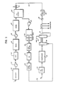
- Figure 1 shows a system for providing the ozonated, deionized purified water.
- raw water is pretreated using multi-media filters and some chemical injection in pretreatment state 10 and is then pumped via pump 12 to a reverse osmosis module 14 from where (if required) it is degasified by degasifier 16 and pumped by repressurization pump 18 to a demineralization state 20 which comprises a cation, anion and mixed bed, or mixed bed alone.
- a double pass reverse osmosis system can be utilized as disclosed in Pittner U.S. Patent No. 4,574,049.
- Demineralized water goes to deionized water storage tank 22. It is repressurized by means of pump 24 and fed to polishing dionized exchange bottles 26 which comprise mixed beds (typically a combination of cation and anion resins).
- the deionized water from mixed beds 26 are filtered via postfilter 28 and then processed through ultraviolet lamps 30 for bacteria control and then through submicron filtration 32.
- the postfilters are used as resin traps.
- the deionized purified water is fed via conduit 34 to a static gas injector 36.
- the deionized purified water is ozonated as follows. Pure oxygen fas is fed through a conventional ozone generator 38 which produces oxygen plus ozone at about 10 psi. The oxygen and ozone at about 10 psi are fed to a compressor 40 where the gas is compressed to 85 psi and then fed to static gas injector 36. The compressed oxygen and ozone will mix with the purified water in the static gas injector 36 to form ozonated water and provide the ozonated water on conduit 42. A bleed line 44 is provided to remove the bubbles from the ozonatede water line.
- the deionized, ozonated, purified water in conduit 42 is fed to the circuit fabrication area, via PVDF plumbing.
- a dissolved ozone meter 46 is provided to monitor the ozone concentration.
- the ozone concentration in the deionized purified water is preferably between .01 and .1 parts per million in order for the wafer during circuit fabrication to be conditioned properly and to prevent significant damage to the system hardware.
- the deionized, ozonated, purified water is recycled but the ozone must be removed prior to return of the water to deionized storage tank 22.
- the ozonated water is processed through ultraviolet lamps 48 for removal of the ozone for recycling.
- the deionized purified water, with the ozone removed, is then fed via conduit 50 through a back pressure regulator 52 to the deionized water storage tank 22.
- Figures 2A - 2N show a portion of the fabrication of the integrated circuit after a clean silicon wafer has been received.
- Figure 2A illustrates the silicon wafer as it may be received from a wafer manufacturer with the silicon wafer 60 being coated with an oxide 62 that is chemically grown or from the previous hydrogen peroxide treatment, with the oxide typically having a thickness of 20 to 30 angstroms. Often the circuit fabricator will remove the oxide to reclean the silicon.
- the oxide layered silicon of Figure 2A may be placed in a furnace where it is oxygeneated to provide a thermally grown oxide 64 (Figure 2B) having a thickness between 100 angstroms and 400 angstroms. Thereafter, a silicon nitride overlayer 66 ( Figure 2C) is provided in a furnace and a photoresist layer 68 is placed over the silicon nitride layer 66.
- the photoresist 68 is illuminated and then etched (see Figure 2E) to leave uncovered portions of the silicon nitride.
- the item of Figure 2E is then conditioned by rinsing it with the deionized purified water containing between .01 and .1 ppm ozone, preferably between .02 and .09 ppm ozone.
- the portions of the silicon nitride 66 that are no longer covered with photoresist 68 are etched to result in the item illustrated in Figure 2F, in which the photoresist has been removed and portions of the oxide 64 are exposed.
- the item is again conditioned by rinsing it with the ozonated water. Thereafter the item is placed in a furnace to provide a thick film oxide 70, approximately 2,000 angstroms thick, which grows where the nitride has been removed. This is illustrated in Figure 2G. Thereafter, the item is conditioned by rinsing it with the ozonated water and the silicon nitride 66 is removed (see Figure 2H).
- a photoresist 68 is added (Figure 2I), illuminated and thereafter etched ( Figure 2I). As illustrated in Figure 2J, this leaves bare portions of the oxide, and the item is again conditioned by rinsing with the ozonated water. As illustrated in Figure 2K, the photoresist is removed and the oxide is etched down to bare silicon in various areas of the silicon surface. Thereafter, as illustrated in Figure 2L, a gate oxide 72 is thermally grown, with the gate oxide having a close tolerance thickness within the range of 150 angstroms to 300 angstroms. The gate oxide is typically the most critical oxidation in the entire fabrication of the integrated circuit. It is absolutely essential that the bare silicon be properly conditioned for the growing of the gate. To this end, the ozonated water rinse treats and conditions the bare silicon and provides a thin oxide layer of perhaps a few monolayers for receiving the gate oxide.
- a layer 74 of polysilicon is deposited.
- another photoresist layer 68 is provided which is illuminated, etched, rinsed with ozonated water, and then the uncovered polysilicon layer is etched and rinsed with the ozonated water, to result in the item illustrated in Figure 2N.
- the conditioning with the ozonated water occur after the material which is no longer covered with photoresist has been etched.
- the conditioning step be performed by rinsing with deionized, purified water containing .01 to .1 ppm ozone, preferably .02 to .09 ppm ozone.
Abstract
Description
- The present invention concerns a process used in the manufacturing of integrated circuits and semiconductor materials.
- In the production of integrated circuits such as VLSI circuits, it is essential that the materials and the circuit being constructed be free from contamination. The numerous steps that are required in producing the silicon wafer and fabricating the circuit render contamination inevitable unless significant precautions and procedures are utilized.
- In the art of manufacturing the silicon waters, the silicon crystal is first grown. The crystal is cropped for specification, and then ground into a cylinder. The cylinder is sliced into thin slices (i.e., wafers), with the thickness of the slices being dependent upon the diameter of the cylinder. The slices are then lapped flat, etch ground and contoured, and then initially cleaned. They are then etched for smoothness and to remove damage, thereafter cleaned again, then polished, and then etched and cleaned. In the latter cleaning process, a hydrogen peroxide solution is used to provide a thin oxide coating (e.g., about 25 to 30 angstroms) and the item is rinsed with a purified water solution. Thereafter, the wafers are packaged in a sterile manner and shipped for circuit fabrication.
- Circuit fabrication is a complex process which requires numerous steps in which thin film materials are layered on a silicon wafer. During the fabrication process, bare portions of the silicon wafer surface may become exposed. These exposed areas become critical functioning parts of the circuit and if the bare silicon is contaminated in any manner, there may be subsequent circuit failure which cannot be detected until the circuit is tested. For example, not only is there a critical interface between the bare silicon and a subsequent oxide layer thereon, but there is also a critical interface between the silicon oxide and a polysilicon coating; between the polysilicon coating and the silicide or metallic coating; and many other interfaces. It is essential that the bare silicon and the interfaces be free from contaminants.
- Some contamination has more negative effects on the functionality of the circuit elements than other contamination. In general, the impact can be defined as either lithographically blocking or chemically contaminating. Particles which are approximately 10 percent to 30 percent of the minimum feature size and optically opaque may significantly alter the functional performance of the circuit element because they alter the lithographic reproduction process. Even smaller particles reduce yield if they chemically alter the silicon near the front surface, or the composition of the films being deposited on the silicon wafer. The greatest problems involve degradation of the quality of the oxide used for gate elements or the polysilicon deposition used for the gate plates or contacts. These contamination problems may not cause immediate functional failure and loss of die yield, but may show up as oxide or contact reliability problems after the die is shipped to the customer.
- Typically, deionized water is used to clean the wafer during the fabrication of the circuit, including cleaning the bare silicon, and cleaning the material interfaces during the fabrication of the device.
- The silicon wafer and the entire integrated circuit process is oxide compatible. It is, therefore, an object of the invention to condition the silicon wafer during fabrication of the integrated circuit, in a manner so that it has the cleanest possible oxide layer on the bare silicon and so that it is most receptive to the next layer to be applied.
- Another object of the present invention is to provide a process for manufacturing integrated circuits in which the wafer is conditioned during critical interfaces to minimize problems at the interfaces and produce a better yield.
- Other objects of the present invention will become apparent as the description proceeds.
- We have discovered that in fabricating the integrated circuit on the wafer, it is beneficial to condition the wafer by rinsing it with purified water containing at least .01 ppm ozone to clean the bare surface of the silicon and between various interfaces of the circuit construction. We have found that such conditioning minimizes contamination by minimizing the adhesion of organics, and minimizes the adhesion of particulates including bacterial particles.
- A process is provided in accordance with the present invention, for manufacturing an integrated circuit in which there are multiple patterned layers of thin film materials on a semiconductor wafer, including the steps of providing a material layer overlying the semiconductor wafer surface; providing a photoresist layer over the material layer; exposing the photoresist to change its characteristics; removing portions of the photoresist to provide uncovered portions of the material layer; removing the uncovered portions of the material layer; and thereafter conditioning the item by rinsing with a purified water solution containing at least .01 ppm ozone.
- In the illustrative embodiment, between the steps of removing portions of the photoresist and removing the uncovered portions of the material layer, the item is also conditioned with a purified water solution containing at least .01 ppm ozone.
- In the illustrative embodiment, the purified water solution preferably contains between 0.02 and .09 ppm ozone. The semiconductor wafer material is silicon, although the process may also be applicable to fabricating an integrated circuit on gallium arsenide.
- A more detailed explanation of the invention is provided in the following description and claims, and is illustrated in the accompanying drawings, wherein:-
- Figure 1 is a block diagram of a water treatment process constructed in accordance with the present invention, used in providing ozonized water for fabricating integrated circuits on silicon wafers;
- Figures 2A - 2N comprise cross-sectional diagrammatic views of the silicon water during circuit fabrication.
- In accordance with the present invention, ozonated and deionized purified water is used for conditioning the wafer during circuit fabrication, to clean the bare surface of the silicon and between various interfaces of the circuit construction. Figure 1 shows a system for providing the ozonated, deionized purified water. Referring to Figure 1, raw water is pretreated using multi-media filters and some chemical injection in
pretreatment state 10 and is then pumped viapump 12 to areverse osmosis module 14 from where (if required) it is degasified bydegasifier 16 and pumped byrepressurization pump 18 to ademineralization state 20 which comprises a cation, anion and mixed bed, or mixed bed alone. - As a substitute for the reverse osmosis module,
degasification stage 16,repressurization pump 18 anddemineralizer 20, which comprises a cation, anion and mixed bed, or mixed bed alone, a double pass reverse osmosis system can be utilized as disclosed in Pittner U.S. Patent No. 4,574,049. - Demineralized water goes to deionized
water storage tank 22. It is repressurized by means ofpump 24 and fed to polishing dionizedexchange bottles 26 which comprise mixed beds (typically a combination of cation and anion resins). The deionized water from mixedbeds 26 are filtered viapostfilter 28 and then processed throughultraviolet lamps 30 for bacteria control and then throughsubmicron filtration 32. The postfilters are used as resin traps. The deionized purified water is fed viaconduit 34 to astatic gas injector 36. - The deionized purified water is ozonated as follows. Pure oxygen fas is fed through a
conventional ozone generator 38 which produces oxygen plus ozone at about 10 psi. The oxygen and ozone at about 10 psi are fed to acompressor 40 where the gas is compressed to 85 psi and then fed tostatic gas injector 36. The compressed oxygen and ozone will mix with the purified water in thestatic gas injector 36 to form ozonated water and provide the ozonated water onconduit 42. A bleed line 44 is provided to remove the bubbles from the ozonatede water line. - The deionized, ozonated, purified water in
conduit 42 is fed to the circuit fabrication area, via PVDF plumbing. A dissolvedozone meter 46 is provided to monitor the ozone concentration. We have discovered that the ozone concentration in the deionized purified water is preferably between .01 and .1 parts per million in order for the wafer during circuit fabrication to be conditioned properly and to prevent significant damage to the system hardware. We have discovered that it is most desirable for the ozone concentration to be between .02 and .09 ppm. - The deionized, ozonated, purified water is recycled but the ozone must be removed prior to return of the water to deionized
storage tank 22. To this end, the ozonated water is processed throughultraviolet lamps 48 for removal of the ozone for recycling. The deionized purified water, with the ozone removed, is then fed viaconduit 50 through aback pressure regulator 52 to the deionizedwater storage tank 22. - Figures 2A - 2N show a portion of the fabrication of the integrated circuit after a clean silicon wafer has been received. Figure 2A illustrates the silicon wafer as it may be received from a wafer manufacturer with the
silicon wafer 60 being coated with anoxide 62 that is chemically grown or from the previous hydrogen peroxide treatment, with the oxide typically having a thickness of 20 to 30 angstroms. Often the circuit fabricator will remove the oxide to reclean the silicon. On the other hand, the oxide layered silicon of Figure 2A may be placed in a furnace where it is oxygeneated to provide a thermally grown oxide 64 (Figure 2B) having a thickness between 100 angstroms and 400 angstroms. Thereafter, a silicon nitride overlayer 66 (Figure 2C) is provided in a furnace and aphotoresist layer 68 is placed over thesilicon nitride layer 66. - The
photoresist 68 is illuminated and then etched (see Figure 2E) to leave uncovered portions of the silicon nitride. The item of Figure 2E is then conditioned by rinsing it with the deionized purified water containing between .01 and .1 ppm ozone, preferably between .02 and .09 ppm ozone. - After such rinsing, the portions of the
silicon nitride 66 that are no longer covered withphotoresist 68 are etched to result in the item illustrated in Figure 2F, in which the photoresist has been removed and portions of theoxide 64 are exposed. The item is again conditioned by rinsing it with the ozonated water. Thereafter the item is placed in a furnace to provide athick film oxide 70, approximately 2,000 angstroms thick, which grows where the nitride has been removed. This is illustrated in Figure 2G. Thereafter, the item is conditioned by rinsing it with the ozonated water and thesilicon nitride 66 is removed (see Figure 2H). The item is again rinsed with the ozonated water and thereafter aphotoresist 68 is added (Figure 2I), illuminated and thereafter etched (Figure 2I). As illustrated in Figure 2J, this leaves bare portions of the oxide, and the item is again conditioned by rinsing with the ozonated water. As illustrated in Figure 2K, the photoresist is removed and the oxide is etched down to bare silicon in various areas of the silicon surface. Thereafter, as illustrated in Figure 2L, agate oxide 72 is thermally grown, with the gate oxide having a close tolerance thickness within the range of 150 angstroms to 300 angstroms. The gate oxide is typically the most critical oxidation in the entire fabrication of the integrated circuit. It is absolutely essential that the bare silicon be properly conditioned for the growing of the gate. To this end, the ozonated water rinse treats and conditions the bare silicon and provides a thin oxide layer of perhaps a few monolayers for receiving the gate oxide. - After the gate is grown as illustrated in Figure 2L, referring to Figure 2M a layer 74 of polysilicon is deposited. After the polysilicon is deposited, another
photoresist layer 68 is provided which is illuminated, etched, rinsed with ozonated water, and then the uncovered polysilicon layer is etched and rinsed with the ozonated water, to result in the item illustrated in Figure 2N. - There are many other layering steps which occur during the fabrication of the circuit. In accordance with the present invention, there will typically be provided a layer of photoresist, which will be illuminated, etched, the residual will be rinsed with ozonated water, then the material that is not underlying the photoresist will be etched and thereafter rinsed with the ozonated water.
- Although it is desirable that the ozonated water be used for rinsing when the photoresist layer has been removed, it is most essential that the conditioning with the ozonated water occur after the material which is no longer covered with photoresist has been etched. Thus, prior to providing an overlayer of material, it is most essential that the conditioning step be performed by rinsing with deionized, purified water containing .01 to .1 ppm ozone, preferably .02 to .09 ppm ozone.
- We have found that the conditioning by ozonated water as just described enhances the circuit fabrication process enabling a controlled oxidation of the interface with an ultrapure reagent. Contamination is minimized by minimizing the adhesion of organics and particulates including bacterial particles. There are minimal particulates because a very clean gas is being injected into ultrapure water. The purity of the ozone that is injected in the water is much higher than the purity of chemicals that are found in the circuit fabrication line in prior art processing systems.
Claims (10)
applying layers of materials over the semiconductor wafer surface;
removing portions of the materials between the applying steps;
between the removing steps and the applying steps, conditioning the item by rinsing it with a purified water solution containing at least .01 ppm ozone.
providing a material layer overlying the semiconductor wafer surface;
providing a photoresist layer over the material layer;
exposing the photoresist to change its characteristics;
removing portions of the photoresist to provide uncovered portions of the material layer;
removing the uncovered portions of the material layer; and
thereafter conditioning the item by rinsing it with a purified water solution containing at least .01 ppm ozone.
providing a second material layer over the conditioned item;
providing a photoresist layer over the second material layer;
exposing the photoresist to change its characteristics;
removing portions of the photoresist to provide uncovered portions of the second material layer;
removing the uncovered portions of the second material layer; and
thereafter conditioning the item by rinsing it with a purified water solution containing at least .01 ppm ozone.
Applications Claiming Priority (2)
| Application Number | Priority Date | Filing Date | Title |
|---|---|---|---|
| US06/903,022 US4749640A (en) | 1986-09-02 | 1986-09-02 | Integrated circuit manufacturing process |
| US903022 | 1992-06-23 |
Publications (2)
| Publication Number | Publication Date |
|---|---|
| EP0259985A2 true EP0259985A2 (en) | 1988-03-16 |
| EP0259985A3 EP0259985A3 (en) | 1990-05-30 |
Family
ID=25416802
Family Applications (1)
| Application Number | Title | Priority Date | Filing Date |
|---|---|---|---|
| EP87307183A Withdrawn EP0259985A3 (en) | 1986-09-02 | 1987-08-14 | Integrated circuit manufacturing process |
Country Status (14)
| Country | Link |
|---|---|
| US (1) | US4749640A (en) |
| EP (1) | EP0259985A3 (en) |
| KR (1) | KR880004543A (en) |
| CN (1) | CN1006506B (en) |
| AU (1) | AU587341B2 (en) |
| BR (1) | BR8704508A (en) |
| CA (1) | CA1264870A (en) |
| DK (1) | DK423587A (en) |
| FI (1) | FI873795A (en) |
| IL (1) | IL83547A0 (en) |
| IN (1) | IN171016B (en) |
| MY (1) | MY100556A (en) |
| NO (1) | NO873670L (en) |
| PH (1) | PH24686A (en) |
Cited By (8)
| Publication number | Priority date | Publication date | Assignee | Title |
|---|---|---|---|---|
| EP0504431A1 (en) * | 1990-10-09 | 1992-09-23 | CHLORINE ENGINEERS CORP., Ltd. | Method of removing organic coating |
| EP0555098A1 (en) * | 1992-02-07 | 1993-08-11 | Tadahiro Ohmi | Lithographic developer and lithographic process |
| EP0556014A1 (en) * | 1992-02-10 | 1993-08-18 | Tadahiro Ohmi | Lithography process |
| EP0702399A1 (en) * | 1994-09-14 | 1996-03-20 | Siemens Aktiengesellschaft | Process for wet chemical removal of contaminants from semiconductor crystal surfaces |
| EP0767487A1 (en) * | 1995-10-05 | 1997-04-09 | Texas Instruments Incorporated | Improvements in or relating to semiconductor device fabrication |
| US5803980A (en) * | 1996-10-04 | 1998-09-08 | Texas Instruments Incorporated | De-ionized water/ozone rinse post-hydrofluoric processing for the prevention of silicic acid residue |
| US6007970A (en) * | 1992-02-07 | 1999-12-28 | Canon Kabushiki Kaisha | Lithographic developer containing surfactant |
| US7271109B2 (en) | 1994-09-26 | 2007-09-18 | Semiconductor Energy Laboratory Co., Ltd. | Solution applying apparatus and method |
Families Citing this family (28)
| Publication number | Priority date | Publication date | Assignee | Title |
|---|---|---|---|---|
| US5181985A (en) * | 1988-06-01 | 1993-01-26 | Wacker-Chemitronic Gesellschaft Fur Elektronik-Grundstoffe Mbh | Process for the wet-chemical surface treatment of semiconductor wafers |
| US4900336A (en) * | 1989-04-03 | 1990-02-13 | Arrowhead Industrial Water, Inc. | Method of preferentially removing oxygen from ozonated water |
| US5190627A (en) * | 1989-11-07 | 1993-03-02 | Ebara Corporation | Process for removing dissolved oxygen from water and system therefor |
| US5378317A (en) * | 1990-10-09 | 1995-01-03 | Chlorine Engineers Corp., Ltd. | Method for removing organic film |
| US5565378A (en) * | 1992-02-17 | 1996-10-15 | Mitsubishi Denki Kabushiki Kaisha | Process of passivating a semiconductor device bonding pad by immersion in O2 or O3 solution |
| KR970008354B1 (en) * | 1994-01-12 | 1997-05-23 | 엘지반도체 주식회사 | Selective etching method |
| JP2914555B2 (en) * | 1994-08-30 | 1999-07-05 | 信越半導体株式会社 | Cleaning method for semiconductor silicon wafer |
| US5674357A (en) * | 1995-08-30 | 1997-10-07 | Taiwan Semiconductor Manufacturing Company, Ltd. | Semiconductor substrate cleaning process |
| US6245155B1 (en) * | 1996-09-06 | 2001-06-12 | Arch Specialty Chemicals, Inc. | Method for removing photoresist and plasma etch residues |
| DE19701971C1 (en) * | 1997-01-22 | 1998-11-26 | Invent Gmbh Entwicklung Neuer Technologien | Method and device for cleaning substrate surfaces |
| US5882425A (en) * | 1997-01-23 | 1999-03-16 | Semitool, Inc. | Composition and method for passivation of a metallization layer of a semiconductor circuit after metallization etching |
| US5971368A (en) | 1997-10-29 | 1999-10-26 | Fsi International, Inc. | System to increase the quantity of dissolved gas in a liquid and to maintain the increased quantity of dissolved gas in the liquid until utilized |
| US6100198A (en) * | 1998-02-27 | 2000-08-08 | Micron Technology, Inc. | Post-planarization, pre-oxide removal ozone treatment |
| US6183637B1 (en) | 1998-07-23 | 2001-02-06 | Seh America, Inc. | Resin trap device for use in ultrapure water systems and method of purifying water using same |
| US6235641B1 (en) | 1998-10-30 | 2001-05-22 | Fsi International Inc. | Method and system to control the concentration of dissolved gas in a liquid |
| US6406551B1 (en) | 1999-05-14 | 2002-06-18 | Fsi International, Inc. | Method for treating a substrate with heat sensitive agents |
| US6790783B1 (en) * | 1999-05-27 | 2004-09-14 | Micron Technology, Inc. | Semiconductor fabrication apparatus |
| US6408535B1 (en) | 1999-08-26 | 2002-06-25 | Semitool, Inc. | Ozone conversion in semiconductor manufacturing |
| US6805791B2 (en) * | 2000-09-01 | 2004-10-19 | Applied Science And Technology, Inc. | Ozonated water flow and concentration control apparatus |
| US6387804B1 (en) | 2000-09-19 | 2002-05-14 | Advanced Micro Devices, Inc. | Passivation of sidewall spacers using ozonated water |
| TW541584B (en) * | 2001-06-01 | 2003-07-11 | Semiconductor Energy Lab | Semiconductor film, semiconductor device and method for manufacturing same |
| US6812064B2 (en) * | 2001-11-07 | 2004-11-02 | Micron Technology, Inc. | Ozone treatment of a ground semiconductor die to improve adhesive bonding to a substrate |
| US7365403B1 (en) * | 2002-02-13 | 2008-04-29 | Cypress Semiconductor Corp. | Semiconductor topography including a thin oxide-nitride stack and method for making the same |
| US7502114B2 (en) * | 2004-03-12 | 2009-03-10 | Mks Instruments, Inc. | Ozone concentration sensor |
| US20060011214A1 (en) * | 2004-07-09 | 2006-01-19 | Zhi Liu | System and method for pre-gate cleaning of substrates |
| JP5251184B2 (en) * | 2008-03-14 | 2013-07-31 | 栗田工業株式会社 | Gas dissolved water supply system |
| CN101752213B (en) * | 2008-12-08 | 2011-09-07 | 北京有色金属研究总院 | Low temperature heat-treatment process for eliminating water mist on silicon chip surface |
| US9627534B1 (en) * | 2015-11-20 | 2017-04-18 | United Microelectronics Corp. | Semiconductor MOS device having a dense oxide film on a spacer |
Citations (6)
| Publication number | Priority date | Publication date | Assignee | Title |
|---|---|---|---|---|
| DE2364135A1 (en) * | 1973-01-02 | 1974-07-11 | Texas Instruments Inc | METHOD AND DEVICE FOR CLEANING THE SURFACE OF AN OBJECTIVE |
| GB1413936A (en) * | 1973-03-30 | 1975-11-12 | Siemens Ag | Production by etching of silicon bodies having patterned silicon dioxide layers thereon |
| DE2928324A1 (en) * | 1979-07-13 | 1981-01-29 | Coolbox Vertriebsgesellschaft | DEVICE FOR MEASURING OZONE IN WATER |
| JPS5953842A (en) * | 1982-09-22 | 1984-03-28 | Seiko Epson Corp | Photographic processing method |
| JPS60239028A (en) * | 1984-05-11 | 1985-11-27 | Nec Corp | Cleaning method of surface |
| JPS614232A (en) * | 1984-06-19 | 1986-01-10 | Nec Corp | Cleaning method of semiconductor substrate |
Family Cites Families (9)
| Publication number | Priority date | Publication date | Assignee | Title |
|---|---|---|---|---|
| US3066050A (en) * | 1960-03-23 | 1962-11-27 | Philco Corp | Fabrication of semiconductor devices |
| US3705055A (en) * | 1970-09-18 | 1972-12-05 | Western Electric Co | Method of descumming photoresist patterns |
| US3890176A (en) * | 1972-08-18 | 1975-06-17 | Gen Electric | Method for removing photoresist from substrate |
| US4156619A (en) * | 1975-06-11 | 1979-05-29 | Wacker-Chemitronic Gesellschaft Fur Elektronik-Grundstoffe Mbh | Process for cleaning semi-conductor discs |
| US4341592A (en) * | 1975-08-04 | 1982-07-27 | Texas Instruments Incorporated | Method for removing photoresist layer from substrate by ozone treatment |
| US4129457A (en) * | 1977-05-23 | 1978-12-12 | International Business Machines Corporation | Post-polishing cleaning of semiconductor surfaces |
| US4318749A (en) * | 1980-06-23 | 1982-03-09 | Rca Corporation | Wettable carrier in gas drying system for wafers |
| US4443295A (en) * | 1983-06-13 | 1984-04-17 | Fairchild Camera & Instrument Corp. | Method of etching refractory metal film on semiconductor structures utilizing triethylamine and H2 O2 |
| US4595498A (en) * | 1984-12-27 | 1986-06-17 | Thomson Components-Mostek Corporation | Water-polishing loop |
-
1986
- 1986-09-02 US US06/903,022 patent/US4749640A/en not_active Expired - Fee Related
-
1987
- 1987-08-11 CA CA000544260A patent/CA1264870A/en not_active Expired - Fee Related
- 1987-08-12 IN IN703/DEL/87A patent/IN171016B/en unknown
- 1987-08-13 DK DK423587A patent/DK423587A/en not_active Application Discontinuation
- 1987-08-13 AU AU76833/87A patent/AU587341B2/en not_active Ceased
- 1987-08-14 IL IL83547A patent/IL83547A0/en unknown
- 1987-08-14 EP EP87307183A patent/EP0259985A3/en not_active Withdrawn
- 1987-08-25 PH PH35733A patent/PH24686A/en unknown
- 1987-08-27 KR KR870009395A patent/KR880004543A/en not_active Application Discontinuation
- 1987-08-28 MY MYPI87001474A patent/MY100556A/en unknown
- 1987-09-01 BR BR8704508A patent/BR8704508A/en unknown
- 1987-09-01 NO NO873670A patent/NO873670L/en unknown
- 1987-09-01 FI FI873795A patent/FI873795A/en not_active Application Discontinuation
- 1987-09-01 CN CN87106114A patent/CN1006506B/en not_active Expired
Patent Citations (6)
| Publication number | Priority date | Publication date | Assignee | Title |
|---|---|---|---|---|
| DE2364135A1 (en) * | 1973-01-02 | 1974-07-11 | Texas Instruments Inc | METHOD AND DEVICE FOR CLEANING THE SURFACE OF AN OBJECTIVE |
| GB1413936A (en) * | 1973-03-30 | 1975-11-12 | Siemens Ag | Production by etching of silicon bodies having patterned silicon dioxide layers thereon |
| DE2928324A1 (en) * | 1979-07-13 | 1981-01-29 | Coolbox Vertriebsgesellschaft | DEVICE FOR MEASURING OZONE IN WATER |
| JPS5953842A (en) * | 1982-09-22 | 1984-03-28 | Seiko Epson Corp | Photographic processing method |
| JPS60239028A (en) * | 1984-05-11 | 1985-11-27 | Nec Corp | Cleaning method of surface |
| JPS614232A (en) * | 1984-06-19 | 1986-01-10 | Nec Corp | Cleaning method of semiconductor substrate |
Non-Patent Citations (3)
| Title |
|---|
| PATENT ABSTRACTS OF JAPAN. vol. 10, no. 85 (E-395)(2152) 12 April 1986; & JP-A-60 239 028 (NIPPON DENKI K.K.) 27-11-1985 * |
| PATENT ABSTRACTS OF JAPAN; vol. 10, no. 141 (E-406)(2198) 24 May 1986; & JP-A-61 004 232 (NIPPON DENKI K.K.) 10-01-1986 * |
| PATENT ABSTRACTS OF JAPAN; vol. 8, no. 157 (P-288)(1594) 20 July 1984; & JP-A-59 053 842 (SUWA SEIKOSHA K.K.) 28-03-1984 * |
Cited By (10)
| Publication number | Priority date | Publication date | Assignee | Title |
|---|---|---|---|---|
| EP0504431A1 (en) * | 1990-10-09 | 1992-09-23 | CHLORINE ENGINEERS CORP., Ltd. | Method of removing organic coating |
| EP0504431A4 (en) * | 1990-10-09 | 1993-03-10 | Chlorine Engineers Corp., Ltd. | Method of removing organic coating |
| EP0555098A1 (en) * | 1992-02-07 | 1993-08-11 | Tadahiro Ohmi | Lithographic developer and lithographic process |
| US6007970A (en) * | 1992-02-07 | 1999-12-28 | Canon Kabushiki Kaisha | Lithographic developer containing surfactant |
| EP0556014A1 (en) * | 1992-02-10 | 1993-08-18 | Tadahiro Ohmi | Lithography process |
| US6107007A (en) * | 1992-02-10 | 2000-08-22 | Canon Kabushiki Kaisha | Lithography process |
| EP0702399A1 (en) * | 1994-09-14 | 1996-03-20 | Siemens Aktiengesellschaft | Process for wet chemical removal of contaminants from semiconductor crystal surfaces |
| US7271109B2 (en) | 1994-09-26 | 2007-09-18 | Semiconductor Energy Laboratory Co., Ltd. | Solution applying apparatus and method |
| EP0767487A1 (en) * | 1995-10-05 | 1997-04-09 | Texas Instruments Incorporated | Improvements in or relating to semiconductor device fabrication |
| US5803980A (en) * | 1996-10-04 | 1998-09-08 | Texas Instruments Incorporated | De-ionized water/ozone rinse post-hydrofluoric processing for the prevention of silicic acid residue |
Also Published As
| Publication number | Publication date |
|---|---|
| KR880004543A (en) | 1988-06-04 |
| CN1006506B (en) | 1990-01-17 |
| IL83547A0 (en) | 1988-01-31 |
| DK423587D0 (en) | 1987-08-13 |
| NO873670D0 (en) | 1987-09-01 |
| CN87106114A (en) | 1988-05-04 |
| MY100556A (en) | 1990-11-15 |
| DK423587A (en) | 1988-03-03 |
| EP0259985A3 (en) | 1990-05-30 |
| FI873795A0 (en) | 1987-09-01 |
| FI873795A (en) | 1988-03-03 |
| BR8704508A (en) | 1988-04-19 |
| AU587341B2 (en) | 1989-08-10 |
| PH24686A (en) | 1990-09-07 |
| AU7683387A (en) | 1988-03-10 |
| US4749640A (en) | 1988-06-07 |
| CA1264870A (en) | 1990-01-23 |
| IN171016B (en) | 1992-07-04 |
| NO873670L (en) | 1988-03-03 |
Similar Documents
| Publication | Publication Date | Title |
|---|---|---|
| US4749640A (en) | Integrated circuit manufacturing process | |
| KR101431615B1 (en) | Silicon surface preparation | |
| US5868855A (en) | Surface processing method and surface processing device for silicon substrates | |
| US6290777B1 (en) | Method and device for washing electronic parts member, or the like | |
| JPH041679B2 (en) | ||
| US9136104B2 (en) | Method for cleaning silicon wafer and apparatus for cleaning silicon wafer | |
| KR100880074B1 (en) | Fabrication method of semiconductor integrated circuit device | |
| US5139623A (en) | Method of forming oxide film on stainless steel | |
| JPH1064867A (en) | Method and device for cleaning a variety of electronic component members | |
| US20060042654A1 (en) | Semiconductor wafer treatment method and apparatus therefor | |
| JP2711389B2 (en) | Integrated circuit manufacturing method | |
| KR101066461B1 (en) | Ultra pure water preparing system and operating method thereof | |
| JP3332323B2 (en) | Cleaning method and cleaning device for electronic component members | |
| US20050211632A1 (en) | Base dosing water purification system and method | |
| JP2000290693A (en) | Cleaning of electronic parts and members | |
| JP3639102B2 (en) | Wet processing equipment | |
| JPH10128253A (en) | Washing method for electronic members and device therefor | |
| US6416676B1 (en) | Deionized water degasification for semiconductor fabrication | |
| JPH07265855A (en) | Production of ultrapure water | |
| US20230174394A1 (en) | Treatment of slurry copper wastewater with ultrafiltration and ion exchange | |
| Gaudet | Point-Of-Use Ultrafiltration of Deionized Rinse Water and Effects on Microelectronics Device Quality | |
| KR100511915B1 (en) | Method for cleaning polishing wafer | |
| JP2004296997A (en) | Method for manufacturing semiconductor integrated circuit device | |
| Ohya | State of the art ultrapure water production in Japan | |
| KR100614643B1 (en) | Ultra pure water production apparatus |
Legal Events
| Date | Code | Title | Description |
|---|---|---|---|
| PUAI | Public reference made under article 153(3) epc to a published international application that has entered the european phase |
Free format text: ORIGINAL CODE: 0009012 |
|
| 17P | Request for examination filed |
Effective date: 19870825 |
|
| AK | Designated contracting states |
Kind code of ref document: A2 Designated state(s): AT BE CH DE ES FR GB GR IT LI LU NL SE |
|
| PUAL | Search report despatched |
Free format text: ORIGINAL CODE: 0009013 |
|
| AK | Designated contracting states |
Kind code of ref document: A3 Designated state(s): AT BE CH DE ES FR GB GR IT LI LU NL SE |
|
| 17Q | First examination report despatched |
Effective date: 19910916 |
|
| STAA | Information on the status of an ep patent application or granted ep patent |
Free format text: STATUS: THE APPLICATION IS DEEMED TO BE WITHDRAWN |
|
| 18D | Application deemed to be withdrawn |
Effective date: 19920327 |
|
| RIN1 | Information on inventor provided before grant (corrected) |
Inventor name: TREMONT, PETER L. Inventor name: ACKERMANN, ARTHUR J. |