EP0065599A1 - Infrared imaging system with infrared detector matrix, and method of imaging infrared energy - Google Patents
Infrared imaging system with infrared detector matrix, and method of imaging infrared energy Download PDFInfo
- Publication number
- EP0065599A1 EP0065599A1 EP81302215A EP81302215A EP0065599A1 EP 0065599 A1 EP0065599 A1 EP 0065599A1 EP 81302215 A EP81302215 A EP 81302215A EP 81302215 A EP81302215 A EP 81302215A EP 0065599 A1 EP0065599 A1 EP 0065599A1
- Authority
- EP
- European Patent Office
- Prior art keywords
- charge
- infrared
- detector elements
- detector
- electrodes
- Prior art date
- Legal status (The legal status is an assumption and is not a legal conclusion. Google has not performed a legal analysis and makes no representation as to the accuracy of the status listed.)
- Granted
Links
- 239000011159 matrix material Substances 0.000 title claims abstract description 17
- 238000000034 method Methods 0.000 title claims abstract description 8
- 238000003331 infrared imaging Methods 0.000 title claims description 16
- 238000003384 imaging method Methods 0.000 title claims description 4
- 238000012546 transfer Methods 0.000 claims abstract description 19
- 238000012545 processing Methods 0.000 claims abstract description 7
- 239000004065 semiconductor Substances 0.000 claims description 21
- 239000000758 substrate Substances 0.000 claims description 20
- 239000012212 insulator Substances 0.000 claims description 19
- 230000004888 barrier function Effects 0.000 claims description 11
- 239000000463 material Substances 0.000 claims description 8
- 238000009413 insulation Methods 0.000 claims description 7
- 239000011810 insulating material Substances 0.000 claims description 5
- 230000003213 activating effect Effects 0.000 claims 1
- 238000002347 injection Methods 0.000 abstract description 8
- 239000007924 injection Substances 0.000 abstract description 8
- 230000008569 process Effects 0.000 abstract description 6
- 238000003860 storage Methods 0.000 abstract description 2
- 230000007246 mechanism Effects 0.000 abstract 2
- 230000010748 Photoabsorption Effects 0.000 abstract 1
- 230000004913 activation Effects 0.000 abstract 1
- 239000002800 charge carrier Substances 0.000 abstract 1
- 229910000661 Mercury cadmium telluride Inorganic materials 0.000 description 9
- 230000010354 integration Effects 0.000 description 8
- 238000001465 metallisation Methods 0.000 description 8
- 239000000969 carrier Substances 0.000 description 7
- PXHVJJICTQNCMI-UHFFFAOYSA-N Nickel Chemical compound [Ni] PXHVJJICTQNCMI-UHFFFAOYSA-N 0.000 description 6
- 229910052751 metal Inorganic materials 0.000 description 5
- 239000002184 metal Substances 0.000 description 5
- 230000004044 response Effects 0.000 description 5
- 238000005070 sampling Methods 0.000 description 5
- 229910052782 aluminium Inorganic materials 0.000 description 4
- XAGFODPZIPBFFR-UHFFFAOYSA-N aluminium Chemical compound [Al] XAGFODPZIPBFFR-UHFFFAOYSA-N 0.000 description 4
- 230000015556 catabolic process Effects 0.000 description 4
- 230000003287 optical effect Effects 0.000 description 4
- XUIMIQQOPSSXEZ-UHFFFAOYSA-N Silicon Chemical compound [Si] XUIMIQQOPSSXEZ-UHFFFAOYSA-N 0.000 description 3
- 229910045601 alloy Inorganic materials 0.000 description 3
- 239000000956 alloy Substances 0.000 description 3
- 238000013461 design Methods 0.000 description 3
- 230000005684 electric field Effects 0.000 description 3
- 239000007943 implant Substances 0.000 description 3
- 239000012535 impurity Substances 0.000 description 3
- 229910052759 nickel Inorganic materials 0.000 description 3
- 229910052710 silicon Inorganic materials 0.000 description 3
- 239000010703 silicon Substances 0.000 description 3
- 230000000712 assembly Effects 0.000 description 2
- 238000000429 assembly Methods 0.000 description 2
- 238000010586 diagram Methods 0.000 description 2
- 238000009792 diffusion process Methods 0.000 description 2
- 230000000694 effects Effects 0.000 description 2
- 230000004907 flux Effects 0.000 description 2
- 229910052738 indium Inorganic materials 0.000 description 2
- APFVFJFRJDLVQX-UHFFFAOYSA-N indium atom Chemical compound [In] APFVFJFRJDLVQX-UHFFFAOYSA-N 0.000 description 2
- 150000002500 ions Chemical class 0.000 description 2
- JVTAAEKCZFNVCJ-UHFFFAOYSA-N lactic acid Chemical compound CC(O)C(O)=O JVTAAEKCZFNVCJ-UHFFFAOYSA-N 0.000 description 2
- QSHDDOUJBYECFT-UHFFFAOYSA-N mercury Chemical compound [Hg] QSHDDOUJBYECFT-UHFFFAOYSA-N 0.000 description 2
- 229910052753 mercury Inorganic materials 0.000 description 2
- 239000000203 mixture Substances 0.000 description 2
- 229910000673 Indium arsenide Inorganic materials 0.000 description 1
- 238000010521 absorption reaction Methods 0.000 description 1
- 238000002048 anodisation reaction Methods 0.000 description 1
- 230000015572 biosynthetic process Effects 0.000 description 1
- 229910052793 cadmium Inorganic materials 0.000 description 1
- BDOSMKKIYDKNTQ-UHFFFAOYSA-N cadmium atom Chemical compound [Cd] BDOSMKKIYDKNTQ-UHFFFAOYSA-N 0.000 description 1
- 239000003990 capacitor Substances 0.000 description 1
- 230000008859 change Effects 0.000 description 1
- 238000010276 construction Methods 0.000 description 1
- 238000001514 detection method Methods 0.000 description 1
- 230000005669 field effect Effects 0.000 description 1
- 229910052732 germanium Inorganic materials 0.000 description 1
- GNPVGFCGXDBREM-UHFFFAOYSA-N germanium atom Chemical compound [Ge] GNPVGFCGXDBREM-UHFFFAOYSA-N 0.000 description 1
- WPYVAWXEWQSOGY-UHFFFAOYSA-N indium antimonide Chemical compound [Sb]#[In] WPYVAWXEWQSOGY-UHFFFAOYSA-N 0.000 description 1
- RPQDHPTXJYYUPQ-UHFFFAOYSA-N indium arsenide Chemical compound [In]#[As] RPQDHPTXJYYUPQ-UHFFFAOYSA-N 0.000 description 1
- 238000005468 ion implantation Methods 0.000 description 1
- 235000014655 lactic acid Nutrition 0.000 description 1
- 239000004310 lactic acid Substances 0.000 description 1
- 238000004519 manufacturing process Methods 0.000 description 1
- 238000007567 mass-production technique Methods 0.000 description 1
- 238000012986 modification Methods 0.000 description 1
- 230000004048 modification Effects 0.000 description 1
- 230000010363 phase shift Effects 0.000 description 1
- 230000005855 radiation Effects 0.000 description 1
- 230000035945 sensitivity Effects 0.000 description 1
- 239000000126 substance Substances 0.000 description 1
- XSOKHXFFCGXDJZ-UHFFFAOYSA-N telluride(2-) Chemical compound [Te-2] XSOKHXFFCGXDJZ-UHFFFAOYSA-N 0.000 description 1
Images


Classifications
-
- H—ELECTRICITY
- H01—ELECTRIC ELEMENTS
- H01L—SEMICONDUCTOR DEVICES NOT COVERED BY CLASS H10
- H01L27/00—Devices consisting of a plurality of semiconductor or other solid-state components formed in or on a common substrate
- H01L27/14—Devices consisting of a plurality of semiconductor or other solid-state components formed in or on a common substrate including semiconductor components sensitive to infrared radiation, light, electromagnetic radiation of shorter wavelength or corpuscular radiation and specially adapted either for the conversion of the energy of such radiation into electrical energy or for the control of electrical energy by such radiation
- H01L27/144—Devices controlled by radiation
- H01L27/146—Imager structures
- H01L27/148—Charge coupled imagers
- H01L27/14862—CID imagers
-
- H—ELECTRICITY
- H01—ELECTRIC ELEMENTS
- H01L—SEMICONDUCTOR DEVICES NOT COVERED BY CLASS H10
- H01L27/00—Devices consisting of a plurality of semiconductor or other solid-state components formed in or on a common substrate
- H01L27/14—Devices consisting of a plurality of semiconductor or other solid-state components formed in or on a common substrate including semiconductor components sensitive to infrared radiation, light, electromagnetic radiation of shorter wavelength or corpuscular radiation and specially adapted either for the conversion of the energy of such radiation into electrical energy or for the control of electrical energy by such radiation
- H01L27/144—Devices controlled by radiation
- H01L27/146—Imager structures
- H01L27/148—Charge coupled imagers
- H01L27/14875—Infrared CCD or CID imagers
-
- H—ELECTRICITY
- H04—ELECTRIC COMMUNICATION TECHNIQUE
- H04N—PICTORIAL COMMUNICATION, e.g. TELEVISION
- H04N25/00—Circuitry of solid-state image sensors [SSIS]; Control thereof
- H04N25/70—SSIS architectures; Circuits associated therewith
- H04N25/76—Addressed sensors, e.g. MOS or CMOS sensors
-
- H—ELECTRICITY
- H04—ELECTRIC COMMUNICATION TECHNIQUE
- H04N—PICTORIAL COMMUNICATION, e.g. TELEVISION
- H04N5/00—Details of television systems
- H04N5/30—Transforming light or analogous information into electric information
- H04N5/33—Transforming infrared radiation
Definitions
- This invention relates to infrared imaging systems and more particularly to an infrared imaging system having an infrared detector matrix utilizing transfer gates.
- infrared detector systems have been of two types staring and non-staring. Staring systems do not require a scanning assembly; while non-staring systems have scanning assemblies. Further, prior art infrared detector systems were transducer type; that is, the impinging infrared energy generated a charge which could be collected and integrated over several frames. The integrated signals were preamplified to provide working signals for video processing. The system is relatively expensive, bulky in size, and inefficient in performance.
- an object of this invention to provide an infrared energy imaging system which leads itself to mass production techniques, is relatively small in size, and has substantially increased efficiency.
- Another object of the invention is to provide an infrared energy imaging system with substantially reduced blooming and crosstalk.
- Still another object of the invention is to increase the charge packet capacity to enable longer integration periods.
- the infrared imaging system comprises an optical assembly, a scanning assembly, an infrared detector matrix, and a video signal processor. If the system is a staring system, the scanning assembly is omitted.
- the optical assembly focuses infrared energy emanating from a scene in its field of view along an optical path where it is scanned by the scanning assembly and the scanned infrared energy impinged onto the infrared detector matrix.
- the infrared detector matrix is a random access imager (RAI) which converts the impinging infrared energy to representative charge packets which are processed into video signals by the video signal processor.
- RAI random access imager
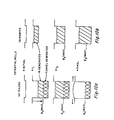
- the forward looking infrared (FLIR) imager (Fig. 1) comprises a lens assembly 12, scanning assembly 14, detector assembly 16, video electronic circuitry 18, and a display 20.
- the scanning assembly 14 is omitted.
- the lens system 12 is comprised of three lens elements, not shown, which for operation in the infrared region are germanium elements. These elements collect infrared energy emanating from a scene and focus this energy onto a rotating mirror, not shown, of the scanning assembly 14.
- the rotating mirror may be, for example, a two sided flat mirror. The first side or front furface, of the mirror is used to receive the infrared energy, and the second side, or rear surface, is used to scan the modulated visible light from the light source 20.
- the scanning mirror is positioned with its "Y" axis normal to the optical axis and its "X" axis at a 45 angle thereto. In this position, the scanning mirror reflects the infrared energy to a folding mirror, not shown, for reflections onto the detector matrix of the detector assembly 16.
- the video electronics circuitry 18 connects each output of the detector array to a light emitting diode, for example, of the light source 20, and provides the signal processing auxillary functions to modulate the output of each light emitting diode.
- the visible light from the light source is directed to impinge upon a folding mirror, not shown, and the folding mirror reflects the visible light through a collimating lens to the second side, or back surface, of the scanning mirror for viewing by an observer.
- the output of the detector matrix might be processed by the video electronics circuitry into a TV format for display on a cathode ray tube.
- Those desiring details of suitable structures for these assemblies, except the detector matrix to be described hereinafter, are referred to U. S. Patent No. 3,Q12,927 issued October 14, 1975, to Richard G. Hoffman, II, for an "Opto-Mechanical Device For Phase Shift Compensation of Oscillating Mirror Scanners.”
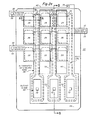
- the random access imager (RAI) 22 comprises a 3 x 3 detector matrix.
- a 3 x 3 detector matrix is disclosed for description purposes only; a 64 x 64 element matrix array is, for example, a more practical design.
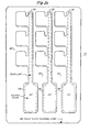
- the detector elements are arranged in rows and columns; the rows of elements being designated, respectively, 24, 26, and 28. Each row of detector elements 24, 26, and 28, are addressed, respectively, through detector address busses 30, 32, and 34.
- the columns of detector. elements 24, 26 and 28 are connected by transfer gates 36, 38, and 40, respectively, to read lines 42, 44, and 46.
- the read lines 42 44, and 46 are connected, respectively, to the output collectors 48, 50, and 52.
- FIG. 3a is a cross section of one detector and adjoining read line taken along line A-A of Figure 2a.
- the rows of detector elements 24, 26 and 28 and transfer gates 36, 38'and 40 are metal/insulator/semiconductor (MIS) structures and the read lines 42, 44, 46, and output collectors 48, 50 and 52 are p-n junctions.
- MIS metal/insulator/semiconductor
- the read lines 42, 44, 46, and output collectors 48, 50 and 52 are p-n junctions.
- a p-type or n-type conductivity semiconductor material may be used for a substrate 54 (Fig. 3a). The particular material used depends on the infrared wavelength to be detected.
- the substrate 54 is of n-type HgCdTe.
- the p-n junction read line 42 is formed, for example, by forming a native oxide layer 56 of a thickness between 0 0 about 500A - 700A on the HgCdTe substrate 54.
- the oxide is formed by anodization.
- the oxide layer 56 is patterned and a via (aperture) etched therein using a lactic acid.
- the junction is then formed by ion implantation, or impurity diffusion, or mercury in-or-out diffusion to form the p-type conductivity region 54'.
- the oxide may be left on after junction formation or stripped off, reoxidized, and the via recut using previously etched alignment marks in the substrate.
- a thin metal layer can be deposited directly on the via to the junction before proceeding with the MIS electrode fabrication. The metal layer forms a via etch stop in the final via etch through a ZnS insulation layer..
- a 500A to 1500A thick layer 58 of insulating material, such as, for example, ZnS is thermally evaporated on top of the native oxide layer 56.
- the ZnS layer 58 is then masked and the field plate/channel stop MIS 0 0 electrode 60 which is, for example, a thick (200A - 1500A) aluminum or nickel electrode patterned on the ZnS layer 58.
- the electrode 60 is preferably formed using the photolithographic lift process. The device as described to this point is shown in Figure 2c.
- the channel-stop MIS structure formed by the substrate 54, insulation layer 58 and channel stop electrode (first level electrode) 60 is covered by a second insulating layer 62 of a 0 0 thickness between 300A - 500A (Fig. 3a).
- the layer 62 is preferably ZnS.
- the second insulating layer 62 is then first metallized, using the photolithographic lift process or a chemical etch to form the thin (150A ) semitransparent electrode 64 for each of the rows of detector elements 24 , 26, and 28 (Fig. 2b) .
- the thin electrodes are preferably nickel electrodes.
- the second insulating layer 62 is then metalized again (Fig.
- a third layer 66 (Fig. 3a) of insulating material 0 (ZnS) is deposited to a thickness between 1000A to 3000A over the metalizations, and then the opaque transfer gate 36, is formed using the photolithographic lift process, to provide the thick 0 0 (1000A-5000A) aluminum electrodes 36, 38, and 40 (Fig. 2c).
- an additional layer 68 (Fig. 3a) (1000A - 5000A) of insulating material (ZnS) is deposited and vias 70 (Fig. 2a) etched to all electrodes and to substrate.
- a soft bonding material such as, for example, indium is used to form bonding pads and expanded contacts touch the desired electrodes through the vias.
- a connection is not required; as it is reset much as a floating source for a MOSFET is reset.
- the random access imager is a metal-insulator -semiconductor (MIS) structure throughout. That is, the read lines 34, 36, and 38 and output collectors 42, 44, and 46 are MIS structures.
- the structure is --identical to that of Figure 3a except in the MIS embodiment the n-type HgCdTe substrate 54 is anodized to form the native oxide layer 56.
- An insulation layer 58 of ZnS is formed over the native oxide layer 56, and the field plate/channel stop 60 and read line electrode 72 of read lines 42, 44 and 46 (Fig. 2a) are formed on the ZnS layer 58 (Fig. 3b).
- the electrode 72 replaces the p-n junction read line of Figure 3a.
- the second ZnS insulating layer 62 covers the field plate/channel stop 60 and read line electrode 72 supported by the first ZnS layer 62.
- the detector element thin electrode 64 and bus 30 are formed on the second ZnS insulating layer and covered by the third ZnS layer 66.
- the third electrode or dc transfer gate 36 is formed on the third ZnS insulating layer 66. The transfer gate 36 provides the guard ring separating the detector element from the read line.
- the MIS structure is also shown in Figure 4, which is a cross section taken along line B-B, Figure 2a.
- the HgCdTe substrate 54 supports the native oxide layer 56 and ZnS insulation layer 58.
- the field plate/channel stop electrode 60 and read line electrode 72 which is contiguous with output collector electrode 74 are metalized on the insulator layer 58 and form the first electrode area.
- the first level metalization is covered by insulation (ZnS) layers 62 and 66; layer 66 supports the transfer gate 36.
- the transfer gate electrode 36 covers the space 76 around the read line and output collector to serve also as a guard ring electrode.
- the contiguous read lines 34, 36 and 38 and output collectors 40, 42, and 44 (Fig.2a), in another embodiment (Fi g. 5), are formed in a spaced relationship by gaps 76 and a pulsed barrier switch 78 utilized to control charge flow through the gaps.
- This embodiment (Fig. 6), which is an MIS structure, includes the HgCdTe 54 substrate supporting the native oxide layer 56 and ZnS insulating layer 58, and the first level metalization formed on the insulation layer 58.
- the first level metalization includes the field plate/channel stop 60, read line electrode 72 and output collector electrode 74.
- the read line electrode 72 and output collector electrode 74 are spaced apart to form the gap 76.
- the first level electrodes are covered by the ZnS insulator layer 62, and the barrier diode electrode 80 is formed on the ZnS layer 62 over the gap 76.
- the ZnS insulator layer 66 covers the barrier diode electrode 80 and the transfer gate 36 is formed on the ZnS insulator layer 66.
- a via 82 (Fig. 5) is etched through the ZnS layer 66 and an indium contact formed therein for electrical connection.
- pulsed barrrier diode 78 makes possible a p-n junction read line and MIS output diode, or an MIS read line and p-n junction output diode.
- the random access imager may be operated in a non-ramped mode or in a ramped mode.
- the RAI (Fig. 7a) includes a horizontal scan generator 84, the detector matrix 22, reset and buffer field effect transistor circuits 86, preamplifier 88 and clamp-sample and hold circuits 90.
- a ramp waveform generator 92 (Fig. 7b) is included between the horizontal scan generator 84 and the RAI 22; otherwise the two structures are the same.
- the horizontal scan generator 84 which is, for example, a ring counter, supplies the waveforms, hereinafter described, to the detector address lines 30, 32, and 34.
- the read lines 36, 38 and 40 and their corresponding output collectors 48, 50 and 52 are each connected to reset and buffer FET circuits 86 (Fig. 7a).
- Reset and buffer FET circuits are also connected to the preamplifiers 88.
- the preamplifiers 88 have their outputs connected to clamp-sample-and-hold circuits 90.
- the RAI output circuitry (Fig. 8) used to sense the charge on each output collector is identical for each column of elements. Thus, only one circuit need be described; the circuit includes either the p-n junction output diode 48 whose anode is connected to source 94 of reset MOSFET 96 or the MIS structure whose electrode is connected to source 94 of reset MOSFET 96.
- MOSFET 96 has its drain 98 connected to a reference voltage and its gate 100 connected to a preset pulse. When a preset pulse is received, the negative reference voltage is applied to the anode of the p-n junction output diode and gate 102 of buffer MOSFET 104.
- Buffer MOSFE T 104 has its source 108 connecterd to a negative V ss voltage and its drain 110 connected to load resistor 112 connected to a positive V DD source and base 114 of bipolar transistor 116.
- Transistor 116 has its emitter 118 connected to the negative V SS voltage and its collector output connected to load resistor 122 connected to the V DD source, and to the input of f the clamp-sample and hold circuit 90.
- an injection pulse capacitor 110 shown in dotted line in Figure 8, is provided.
- the reset and buffer MOSFETS can be in a separate silicon chip adjoining the detector RAI chip or alternatively, the reset and buffer MOSFETS can be built directly on the same chip as the RAI; in this monolithic version using the output diode 48, this diode can be the source of the reset MOSFET.
- Figures 9a, 9b, and 9c show the voltages applied to the detector rows 24, 26, and 28 for the case using n-type material with zero volts being "off" and -Vi or -V 2 "on” and thereby creating a potential well under the row electrodes 24, 26, and 28.
- row wells 24 turn off, row wells 26 turn on, and so forth.
- the turn-off of row 24 and the turn-on of row 26 can be simultaneous or 24 may turn-off slightly before 26 turn on, and so forth.
- the waveforms at the bottom of Figures 9a, 9b, and 9c show the voltage output at 48, 50, and 52.
- the arrows show the timing of the clamp and sample pulses.
- a negative preset voltage pulse is applied during time to - t l to the charge collecting diodes 48, 50, and 52.
- the reset pulse sets the diode to a fixed known voltage prior to dumping charge onto the diode from row 26 detectors.
- the reset pulse is turned off and the voltage on the diodes 48, 50, and 52 are measured and amplified by buffer 104 (Fig. R) and clamped by CS&H circuit 90.
- the row of detector elements 26 is turned off and the charges of their potential wells dumped during time t 2 - t 3 through read lines 42, 44, and 46 (Fig. 2a) into the collector diodes 48, 50 and 52.
- the collector diodes 48, 50 and 52 voltage outputs are buffered and sampled by C S & H circuit 90 ( F ig. 8).
- the clamped voltage is subtracted from the sampled voltage and the difference represents the intensity of the infrared photon flux impinging on the second row of detector elements 26.
- t 3 (which is also to) the second cycle begins with the second row of detector elements being turned on by the second reset pulse for charging.
- the charges of the third row of detector elements 28 have been determined, and the row of detector -elements 28 turned on again.
- the third cycle begins with the row of detector elements 24 being turned off, and at the end of the third cycle the charges of the first row of detector elements 24 have been determined and the first row of detector elements 24 turned on again.
- the cycle continues throughout the RAI operation. Although the selection of rows has been shown in a sequential operation, the rows may be selected randomly.
- the timing and waveforms are shown in Figure 9b.
- a reset pulse is applied to the MIS output elements 48, 50, and 52 to set the potential wells underneath these MIS electrodes to a fixed constant surface potential.
- the reset pulse is turned off.
- the second row of detector elements 26 are turned off and their charges are dumped into the read lines 42, 44, and 46.
- the voltages of the MIS output electrodes 48, 50, and 52 are measured and clamped by the buffer and CS&H circuit (Fig. 8).
- an injection pulse is applied to the barrier gate 78 is turned off slightly prior to t 2 and turned on slightly after 13 . Because the barrier gate is off during the time of the application of the injection pulse, the the charges underneath the MIS output electrodes are injected into the substrate rather than back into the read lines 42 and 44 of Figure 5.
- the charge collectors 48, 50, and 52 are sampled by the CS&H circuit 90 (Fig. 8) and the difference in the clamped and sampled voltages determined.
- This difference voltage represents the intensity of the infrared p ho - ton flux impinging on the rows of detector elements 26:
- a second reset pulse is applied to determine the charges of the third row of detector elements 28.
- the cycle is repeated for a third cycle to determine the charges of the first row of detector elements 24.
- the cycle is continued throughout RAI operation.
- the clamp and sample pulses in Figure 9b are shown centered around the injection pulse and thereby detecting the charge injected into the substrate; in an alternate scheme, the preset pulse can be applied and turned off prior to the turn off of detector row 26 and the clamp and sample pulses centered around the turn off of detector row 26 thereby detecting the charge transferred underneath the output MIS electrodes 48, 50, and 52.
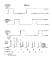
- FIG. 9c When the rows of detectors 24, 26, and 28 are ramped, multiple amplitude voltages are applied as shown in Figure 9c.
- the potential wells are formed by biasing the metal gates 62 (Fig. 3b) of the rows of MIS elements 24, 26 and 28 (Fig. 2a) to a voltage to drive away the majority carriers from the surface of the semiconductor to uncover net impurity charge density Q D in a depletion layer and to permit the collection of mobile carrier charge density Q INV in the potential well with surface density ⁇ g.
- the relationship between ⁇ S V , Q and the insulator capacitance per unit area is:
- V 0 (gN ⁇ 0 ⁇ )/C 2 INS
- V T the threshold for inversion.
- the gate voltages are pulsed between a maximum and a minimum gate voltage.
- the MIS gate voltage V which gives the maximum empty well depth ⁇ S (or electric field E S ) in turn determines the maximum amount of charge Q FW which the well can contain.
- the maximum E S may be set by electric breakdown in the semiconductor. If the maximum E S in the semiconductor is very large, the maximum gate voltage may be set by electric breakdown in the insulator. In the case of silicon MIS devices, the maximum E S is in the range of 10 6 V/cm and the maximum ⁇ S , V , and Q FW are set by electric breakdown in the insulator.
- the maximum permissible electric field in the semiconductor is much smaller in narrow band gap semiconductors such as InSb and InAs and the alloy semiconductors HgCdTe, InAsSb, GaInSb, and PbSnTe.
- the maximum E S is 104 V/cm for an alloy composition to give an infrared response with long wavelength response threshold at 10 ⁇ m and is 3x10⁴ V/ cm for an alloy composition to give a response threshold at 5 ⁇ m.
- the relatively low maximum E S in long wavelength response semiconductors such a HgCdTe severly limits the maximum charge capacity of the well and thereby the maximum integration time, maximum signal, and maximum signal-to-noise ratio of the infrared sensitive CTD.
- Figure 10a shows the standard mode of infrared detection in an MIS well of a CTD array in which the gate voltage is pulsed from an initial low value to a large value to create a potential well in the semiconductor.
- the initial ⁇ S created is given by the depth of the potential wells shown in Figure 10a.
- Figure la shows the case with the initial ⁇ S larger than the tunnel threshold ⁇ S (max) value: in this case, charge very rapidly tunnels to the well to partially fill the well to the dashed line at ⁇ S (max). After this initial tunnel current, the infrared generated minority carriers slowly begin to fill the well as shown for times t 1 and t 2 .
- the potential well overfills as shown at the bottom of Figure la because the tunnel current has reduced the charge capacity available for the storage of infrared generated minority carriers. Signal charge cannot be collected for a time longer than that for which the tunnel and background generated carriers completely fill the well.
- Figure 10b shows the growth of surface potential and stored charge for the ramped MIS over the same times as those shown in Figure 10a.
- the same MIS structure was used for determining the growth of surface potential shown in Figures 10a and 10b.
- the well does not overfill because no tunnel generated charge has appeared in the well.
- Large increases in maximum integration time can be obtained for closely balanced ramps.
- a maximum ramped integration time 17-times longer than that obtained -for a pulsed MIS has been observed for a HgCdTe MIS with a 9.4 m long-wavelength cutoff in a 20° field-of-view for ambient radiation.
- the desired ramp effect t on ⁇ S may be ' improved through device design by utilizing an MIS electrode which has a small opaque region, and which has an inversion threshold slightly smaller than that for the larger area transparent region.
- the first effect of the ramp is to create a small empty well under the opaque electrode which is insensitive to infrared.
- the gate voltage becomes larger than inversion threshold for -the large area transparent gate region of the MIS
- the infrared sensitive potential well starts out partially empty due to the diversion of photogenerated carriers to the opaque portion of the well.
- the ramp rate is chosen so that the surface potential does not increase after the gate voltage is large enough to turn on both portions of the well.
- the difference in flatband voltages between the transparent and opaque portions of the MIS must be smaller than that difference which would cause the potential well underneath the opaque electrode portion from reaching the tunnel threshold before the potential well underneath the transparent electrode portion turns on.
- a preset pulse 122 is applied to set the output collector 48, 50 and 52 to a reference voltage.
- the first row of detector elements 24 are turned off to dump their charges into the read line.
- the clamp sample and hold (CS&H) circuit 56 while clamping period 124, clamps the buffered output of the output collector to hold the voltage of the output collectors 48, 50,and 52.
- an injection pulse 126 is applied to the output MIS collectors 48, 50, and 52 to collapse these wells while simultaneously the barrier gate 78 is closed so that the charges underneath the MIS collectors are injected into the substrate.
- the buffered output of output collectors 48, 50 and 52 during the period 128 are sampled by the CS&H circuit 56 and the voltage difference determined.
- the voltage difference represents the value of the infrared generated charge accumulated in the first row of ramped detector elements 24. If p-n junction diodes 48, 50, and 52 had been used, the output scheme shown at the bottom of Figure 9a could have been used.
- the first row of detector elements 24 are turned on (-Vi) and ramping to voltage (-V 2 ) begun.
- the output collector is set to the reference voltage, and the second row of detector elements 26 are turned off to dump the charge of the second row of the detector elements into the read line.
- the buffered voltages of the output collectors 48, 50 and 52 are clamped by CS&H circuits 90.
- barrier gate 78 is turned off and a second injection pulse 134 applied to the output collectors 48, 50, and 52 and the buffered output, during a sampling period 136, sampled by CS&H circuit 90.
- the voltage difference indicates the infrared generated charge in the second row detector elements 26.
- the ramping of the first row of detector elements 24 continues.
- the second row of detector elements 26 are turned on by a voltage (-V) and the ramping to voltage -V 2 begun.
- the cycle is completed by a third preset pul.se 138 which again sets the collector output to a reference voltage.
- preset the third row of detector elements 28 are turned off to dump their charge into the read line.
- the output collector is clamped during clamping period 140 to receive the outputs of the third row of detectors 28.
- an injection pulse 142 is applied to the collector electrodes 48, 50, and 52 and simulanteously the barrier gate 78 is turned off to dump charges in output charge collectors 48, 50 and 52 into the substrate.
- the buffered outputs of the charge collectors 48, 50, and 52 are sampled during sampling period 144 by the CS&H circuit 90 and the voltage difference represents the value of the infrared energy generated charge on the third row of detector elements 28.
- the ramping of the first - row of detectors 24 is completed, and the ramping of the second row of detectors 26 continues.
- a preset pulse 146 is applied to th£ output collectors 48, 50, and 52 to set them at reference voltage, and the first row of detectors 24 are turned off to dump the charge therein into the read line to start a new cycle of operation.
- the potential wells generated during the three stages (a, b and c) are shown in Figure 4.
- the preferred embodiment utilizes a p-n junction read line 72 of Figure 4 to give rapid flow of the carriers from the detector wells 24, 26, and 28 to the output devices 48, 50, and 52.
- One purpose of the barrier well 80 of Figure 6 is to provide a background charge in the MIS read line to shorten the response time of this read line.
- a threshold shifting ion implant in the region of the dc transfer gates 36, 38, and 40 can be used to form the desired potential in these regions without the use of the dc transfer gates thus eliminating one set of electrodes.
- an ion implant and/or thick insulator is used in the field stop region 60 and this implant and/or insulator are/is sufficient to keep the surface under 60 accumulated, then the field plate/channel stop MIS electrode can be eliminated.
Abstract
Description
- This invention relates to infrared imaging systems and more particularly to an infrared imaging system having an infrared detector matrix utilizing transfer gates.
- In the past, infrared detector systems have been of two types staring and non-staring. Staring systems do not require a scanning assembly; while non-staring systems have scanning assemblies. Further, prior art infrared detector systems were transducer type; that is, the impinging infrared energy generated a charge which could be collected and integrated over several frames. The integrated signals were preamplified to provide working signals for video processing. The system is relatively expensive, bulky in size, and inefficient in performance.
- Accordingly it is an object of this invention to provide an infrared energy imaging system which leads itself to mass production techniques, is relatively small in size, and has substantially increased efficiency.
- Another object of the invention is to provide an infrared energy imaging system with substantially reduced blooming and crosstalk.
- Still another object of the invention is to increase the charge packet capacity to enable longer integration periods.
- Briefly stated the infrared imaging system comprises an optical assembly, a scanning assembly, an infrared detector matrix, and a video signal processor. If the system is a staring system, the scanning assembly is omitted. The optical assembly focuses infrared energy emanating from a scene in its field of view along an optical path where it is scanned by the scanning assembly and the scanned infrared energy impinged onto the infrared detector matrix. The infrared detector matrix is a random access imager (RAI) which converts the impinging infrared energy to representative charge packets which are processed into video signals by the video signal processor.
- The novel features characteristic of this invention are set forth in the appended claims. The invention itself, however, as well as other objects and advantages thereof may best be understood by reference to the following detailed description of illustrative embodiments when read in conjunction with the accompanying drawings in which:
- FIGURE 1 is a block diagram of a forward looking infrared system;
- FIGURE 2a is a plan view of the random access imager (RAI);
- FIGURE 2b is a partial plan view of the RAI of Figure 2a with the transfer gate/guard ring metalization removed to show more clearly the detector elements metalization and connecting buses;
- FIGURE 2c is a partial plan view of the RAI of Figure 2b with detector elements metalization and connecting buses removed to show more clearly the field plate/channel stop metalization over the insulator, semiconductor substrate;
- FIGURE 3a is a cross-sectional view taken along line A-A of Figure 2a;
- FIGURE 3b is a cross-sectional view taken along line A-A of Figure 2a modified to show another embodiment of the read out line;
- FIGURE 4 is a cross-sectional view taken along line B-B of Figure 2a;
- FIGURE 5 is a partial top view of the random access imager showing a second embodiment of the read out line and output diode;
- FIGURE 6 is a cross-sectional view taken input along line B-B of Figure 5 to show the second embodiment of the read out structure extended to show the read line of B-B Figure 2a;
- FIGURES 7a and 7b are block diagrams of the circuitry necessary for an RAI array without ramping and with ramping, respectively;
- FIGURE 8 shows the output circuitry for each output diode of the RAI array;
- FIGURES 9a, 9b, and 9c show, respectively, the timing and address waveforms for the diode and MIS charge collector means without ramping; and MIS charge collector means with ramping; and
- FIGURES 10a and lOb show, respectively, the filling of potential wells without ramping and with ramping over identical integration times.
- Referring now to the drawings, the forward looking infrared (FLIR) imager (Fig. 1) comprises a
lens assembly 12,scanning assembly 14,detector assembly 16, videoelectronic circuitry 18, and adisplay 20. In a staring system, thescanning assembly 14 is omitted. Thelens system 12 is comprised of three lens elements, not shown, which for operation in the infrared region are germanium elements. These elements collect infrared energy emanating from a scene and focus this energy onto a rotating mirror, not shown, of thescanning assembly 14. The rotating mirror may be, for example, a two sided flat mirror. The first side or front furface, of the mirror is used to receive the infrared energy, and the second side, or rear surface, is used to scan the modulated visible light from thelight source 20. The scanning mirror is positioned with its "Y" axis normal to the optical axis and its "X" axis at a 45 angle thereto. In this position, the scanning mirror reflects the infrared energy to a folding mirror, not shown, for reflections onto the detector matrix of thedetector assembly 16. Thevideo electronics circuitry 18 connects each output of the detector array to a light emitting diode, for example, of thelight source 20, and provides the signal processing auxillary functions to modulate the output of each light emitting diode. Finally, the visible light from the light source is directed to impinge upon a folding mirror, not shown, and the folding mirror reflects the visible light through a collimating lens to the second side, or back surface, of the scanning mirror for viewing by an observer. It will be appreciated that the output of the detector matrix might be processed by the video electronics circuitry into a TV format for display on a cathode ray tube. Those desiring details of suitable structures for these assemblies, except the detector matrix to be described hereinafter, are referred to U. S. Patent No. 3,Q12,927 issued October 14, 1975, to Richard G. Hoffman, II, for an "Opto-Mechanical Device For Phase Shift Compensation of Oscillating Mirror Scanners." - Referring now to Figure 2a, the random access imager (RAI) 22 comprises a 3 x 3 detector matrix. A 3 x 3 detector matrix is disclosed for description purposes only; a 64 x 64 element matrix array is, for example, a more practical design. The detector elements are arranged in rows and columns; the rows of elements being designated, respectively, 24, 26, and 28. Each row of
detector elements elements transfer gates lines read lines 42 44, and 46 are connected, respectively, to theoutput collectors - Referring now to Figure 3a which is a cross section of one detector and adjoining read line taken along line A-A of Figure 2a. In the first embodiment of the RAI 22 (Fig. 2a) the rows of
detector elements transfer gates 36, 38'and 40 are metal/insulator/semiconductor (MIS) structures and theread lines output collectors substrate 54 is of n-type HgCdTe. The p-n junction readline 42 is formed, for example, by forming anative oxide layer 56 of a thickness between 0 0 about 500A - 700A on theHgCdTe substrate 54. The oxide is formed by anodization. Theoxide layer 56 is patterned and a via (aperture) etched therein using a lactic acid. The junction is then formed by ion implantation, or impurity diffusion, or mercury in-or-out diffusion to form the p-type conductivity region 54'. - The oxide may be left on after junction formation or stripped off, reoxidized, and the via recut using previously etched alignment marks in the substrate. A thin metal layer, not shown, can be deposited directly on the via to the junction before proceeding with the MIS electrode fabrication. The metal layer forms a via etch stop in the final via etch through a ZnS insulation layer..
- After the p-n junction is formed, a 500A to 1500A
thick layer 58 of insulating material, such as, for example, ZnS is thermally evaporated on top of thenative oxide layer 56. TheZnS layer 58 is then masked and the field plate/channel stopMIS 0 0electrode 60 which is, for example, a thick (200A - 1500A) aluminum or nickel electrode patterned on theZnS layer 58. Theelectrode 60 is preferably formed using the photolithographic lift process. The device as described to this point is shown in Figure 2c. - The channel-stop MIS structure formed by the
substrate 54,insulation layer 58 and channel stop electrode (first level electrode) 60 is covered by a second insulatinglayer 62 of a 0 0 thickness between 300A - 500A (Fig. 3a). Thelayer 62 is preferably ZnS. The second insulatinglayer 62 is then first metallized, using the photolithographic lift process or a chemical etch to form the thin (150A )semitransparent electrode 64 for each of the rows ofdetector elements layer 62 is then metalized again (Fig. 3a) using the photolithographic process to form the thick (200A - 2000A ) opaque metal (aluminum)address lines aluminum address lines thin nickel electrodes 64 to electrically connect the rows ofdetector elements - Next, a third layer 66 (Fig. 3a) of insulating material 0 (ZnS) is deposited to a thickness between 1000A to 3000A over the metalizations, and then the
opaque transfer gate 36, is formed using the photolithographic lift process, to provide the thick 0 0 (1000A-5000A)aluminum electrodes - In a second embodiment (Fig. 3b), which is a cross-section taken along line A-A of Figure 2a, the random access imager is a metal-insulator -semiconductor (MIS) structure throughout. That is, the read lines 34, 36, and 38 and
output collectors type HgCdTe substrate 54 is anodized to form thenative oxide layer 56. Aninsulation layer 58 of ZnS is formed over thenative oxide layer 56, and the field plate/channel stop 60 and readline electrode 72 of readlines electrode 72 replaces the p-n junction read line of Figure 3a. To complete the structure, the secondZnS insulating layer 62 covers the field plate/channel stop 60 and readline electrode 72 supported by thefirst ZnS layer 62. The detector elementthin electrode 64 andbus 30 are formed on the second ZnS insulating layer and covered by thethird ZnS layer 66. The third electrode ordc transfer gate 36 is formed on the thirdZnS insulating layer 66. Thetransfer gate 36 provides the guard ring separating the detector element from the read line. - The MIS structure is also shown in Figure 4, which is a cross section taken along line B-B, Figure 2a. In this structure, the
HgCdTe substrate 54 supports thenative oxide layer 56 andZnS insulation layer 58. The field plate/channel stop electrode 60 and readline electrode 72 which is contiguous withoutput collector electrode 74 are metalized on theinsulator layer 58 and form the first electrode area. The first level metalization is covered by insulation (ZnS) layers 62 and 66;layer 66 supports thetransfer gate 36. Thetransfer gate electrode 36 covers thespace 76 around the read line and output collector to serve also as a guard ring electrode. - The
contiguous read lines output collectors gaps 76 and apulsed barrier switch 78 utilized to control charge flow through the gaps. This embodiment (Fig. 6), which is an MIS structure, , includes theHgCdTe 54 substrate supporting thenative oxide layer 56 andZnS insulating layer 58, and the first level metalization formed on theinsulation layer 58. The first level metalization includes the field plate/channel stop 60, readline electrode 72 andoutput collector electrode 74. The readline electrode 72 andoutput collector electrode 74 are spaced apart to form thegap 76. The first level electrodes are covered by theZnS insulator layer 62, and thebarrier diode electrode 80 is formed on theZnS layer 62 over thegap 76. TheZnS insulator layer 66 covers thebarrier diode electrode 80 and thetransfer gate 36 is formed on theZnS insulator layer 66. A via 82 (Fig. 5) is etched through theZnS layer 66 and an indium contact formed therein for electrical connection. - The use of the
pulsed barrrier diode 78 makes possible a p-n junction read line and MIS output diode, or an MIS read line and p-n junction output diode. - The random access imager (RAI) may be operated in a non-ramped mode or in a ramped mode. In the non-ramped mode, the RAI (Fig. 7a) includes a
horizontal scan generator 84, thedetector matrix 22, reset and buffer fieldeffect transistor circuits 86,preamplifier 88 and clamp-sample and holdcircuits 90. For ramped operation, a ramp waveform generator 92 (Fig. 7b) is included between thehorizontal scan generator 84 and theRAI 22; otherwise the two structures are the same. - In the non-ramped structure the
horizontal scan generator 84, which is, for example, a ring counter, supplies the waveforms, hereinafter described, to thedetector address lines corresponding output collectors preamplifiers 88. Thepreamplifiers 88 have their outputs connected to clamp-sample-and-hold circuits 90. - In the ramped mode (Fig. 7b), each output of the
horizontal scan converter 84 activates aramp waveform generator 92. The waveform generator is, for example, an RC charging circuit followed by an operational amplifier, in this form, the linear portion of the RC rise time is used. In another embodiment, the ramp generator can approximate a linear ramp by providing a series of closely spaced step increases in voltage. - The RAI output circuitry (Fig. 8) used to sense the charge on each output collector is identical for each column of elements. Thus, only one circuit need be described; the circuit includes either the p-n
junction output diode 48 whose anode is connected to source 94 of reset MOSFET 96 or the MIS structure whose electrode is connected to source 94 of reset MOSFET 96. MOSFET 96 has itsdrain 98 connected to a reference voltage and itsgate 100 connected to a preset pulse. When a preset pulse is received, the negative reference voltage is applied to the anode of the p-n junction output diode and gate 102 ofbuffer MOSFET 104. Buffer MOSFET 104 has itssource 108 connecterd to a negative Vss voltage and itsdrain 110 connected to loadresistor 112 connected to a positive VDD source and base 114 ofbipolar transistor 116.Transistor 116 has itsemitter 118 connected to the negative VSS voltage and its collector output connected to loadresistor 122 connected to the VDD source, and to the input of f the clamp-sample and holdcircuit 90. - In the embodiment where the output collector is an MIS structure, an
injection pulse capacitor 110, shown in dotted line in Figure 8, is provided. - The reset and buffer MOSFETS can be in a separate silicon chip adjoining the detector RAI chip or alternatively, the reset and buffer MOSFETS can be built directly on the same chip as the RAI; in this monolithic version using the
output diode 48, this diode can be the source of the reset MOSFET. - Figures 9a, 9b, and 9c show the voltages applied to the
detector rows row electrodes row wells 24 turn off,row wells 26 turn on, and so forth. The turn-off ofrow 24 and the turn-on ofrow 26 can be simultaneous or 24 may turn-off slightly before 26 turn on, and so forth. The waveforms at the bottom of Figures 9a, 9b, and 9c show the voltage output at 48, 50, and 52. The arrows show the timing of the clamp and sample pulses. - Referring now to Figure 9a for a description of the operation of the device when p-n junction type (diode)
collectors - With row of
detector elements 24 off and having already dumped their charges into thecollector diodes detector elements charge collecting diodes row 26 detectors. Next, during the time tl-t2 the reset pulse is turned off and the voltage on thediodes CS&H circuit 90. At the time t2 the row ofdetector elements 26 is turned off and the charges of their potential wells dumped during time t2 - t3 through readlines collector diodes collector diodes detector elements 26. At t3 (which is also to) the second cycle begins with the second row of detector elements being turned on by the second reset pulse for charging. At the end of the second cycle (t3), the charges of the third row ofdetector elements 28 have been determined, and the row of detector -elements 28 turned on again. Then the third cycle begins with the row ofdetector elements 24 being turned off, and at the end of the third cycle the charges of the first row ofdetector elements 24 have been determined and the first row ofdetector elements 24 turned on again. The cycle continues throughout the RAI operation. Although the selection of rows has been shown in a sequential operation, the rows may be selected randomly. - For operation of the MIS embodiment of the RAI, the timing and waveforms are shown in Figure 9b. With row of
detector elements 24 off and having dumped and rows ofdetector elements MIS output elements detector elements 26 are turned off and their charges are dumped into the readlines MIS output electrodes barrier gate 78 is turned off slightly prior to t2 and turned on slightly after 13. Because the barrier gate is off during the time of the application of the injection pulse, the the charges underneath the MIS output electrodes are injected into the substrate rather than back into the readlines charge collectors detector elements 28. Finally, the cycle is repeated for a third cycle to determine the charges of the first row ofdetector elements 24. The cycle is continued throughout RAI operation. The clamp and sample pulses in Figure 9b are shown centered around the injection pulse and thereby detecting the charge injected into the substrate; in an alternate scheme, the preset pulse can be applied and turned off prior to the turn off ofdetector row 26 and the clamp and sample pulses centered around the turn off ofdetector row 26 thereby detecting the charge transferred underneath theoutput MIS electrodes - When the rows of
detectors MIS elements 
- The thickness of the layer containing QINV (less than 16-6 cm) when compared to the thickness of the layer containing QD (greater than 10-4 cm) can be omitted and, OD is written in terms of ψS using V0 = (gNξ0ε)/C2 INS where g is the electronic charge, N the net impurity concentration in the semiconductor, ξ0 is the dielectric permittivity of free space, and ε is the dielectric constant of the semiconductor. The result for a p-type semiconductor with positive V and ψS and with negative QINV is:


- The electric field ES at the surface of the semiconductor is:

- The charge stored in the well is related to ψS or Eg through equation (2). Thus,

- In the case of a full well:

- VT = the threshold for inversion.
- In the usual mode of operation of a CTD, the gate voltages are pulsed between a maximum and a minimum gate voltage. In this mode, the MIS gate voltage V which gives the maximum empty well depth ψS (or electric field ES) in turn determines the maximum amount of charge QFW which the well can contain. The maximum ES may be set by electric breakdown in the semiconductor. If the maximum ES in the semiconductor is very large, the maximum gate voltage may be set by electric breakdown in the insulator. In the case of silicon MIS devices, the maximum ES is in the range of 106 V/cm and the maximum ψS, V, and QFW are set by electric breakdown in the insulator. The maximum permissible electric field in the semiconductor is much smaller in narrow band gap semiconductors such as InSb and InAs and the alloy semiconductors HgCdTe, InAsSb, GaInSb, and PbSnTe. In the case of HgCdTe, the maximum ES is 104 V/cm for an alloy composition to give an infrared response with long wavelength response threshold at 10 µm and is 3x10⁴ V/cm for an alloy composition to give a response threshold at 5 µm. This wavelength threshold may be set by tunnel current IT breakdown which is related to ES and the bandgap EG of the semiconductor

- In detecting either visible or infrared images, photons pass through the semitransparent substrate or semitransparent electrodes and are absorbed in the semiconductor where the absorption process creates minority carriers which can be collected in the CTD potential well. The sensitivity of the CTD as an infrared sensor is proportional to the maximum time (maximum - integration time) the well can collect signal generated charge. The signal-to-noise ratio of the infrared CTD is proportional to the square root of the maximum integration time. Unfortunately, in addition to the infrared signal generated charge, there is a much larger charge generated due to the infrared coming from viewing room temperature background. This infrared background generated charge limits the maximum integration time for signal generated charge. The relatively low maximum ES in long wavelength response semiconductors such a HgCdTe severly limits the maximum charge capacity of the well and thereby the maximum integration time, maximum signal, and maximum signal-to-noise ratio of the infrared sensitive CTD.
- Figure 10a shows the standard mode of infrared detection in an MIS well of a CTD array in which the gate voltage is pulsed from an initial low value to a large value to create a potential well in the semiconductor. The initial ψS created is given by the depth of the potential wells shown in Figure 10a. Figure la shows the case with the initial ψS larger than the tunnel threshold ψS (max) value: in this case, charge very rapidly tunnels to the well to partially fill the well to the dashed line at ψS (max). After this initial tunnel current, the infrared generated minority carriers slowly begin to fill the well as shown for times t1 and t2. Finally, the potential well overfills as shown at the bottom of Figure la because the tunnel current has reduced the charge capacity available for the storage of infrared generated minority carriers. Signal charge cannot be collected for a time longer than that for which the tunnel and background generated carriers completely fill the well.
- When the MIS gate voltage is ramped in the presence of an infrared background which creates a minority carrier current density J0 amps/cm2, QINV increases simultaneously with the increase in
V. Equation 3 shows that if the rate of increase of QINV/CINS just balances the rate dV/dt of increase of V, then the surface potential ψS will not change. Since Jo = -dQINV/dt, the requirement for a constant ψS during the ramp of a partially filled well is
- Figure 10b shows the growth of surface potential and stored charge for the ramped MIS over the same times as those shown in Figure 10a. The same MIS structure was used for determining the growth of surface potential shown in Figures 10a and 10b. In Figure 10b, the well does not overfill because no tunnel generated charge has appeared in the well. Large increases in maximum integration time can be obtained for closely balanced ramps. A maximum ramped integration time 17-times longer than that obtained -for a pulsed MIS has been observed for a HgCdTe MIS with a 9.4 m long-wavelength cutoff in a 20° field-of-view for ambient radiation.
- The desired ramp effect t on ψS may be 'improved through device design by utilizing an MIS electrode which has a small opaque region, and which has an inversion threshold slightly smaller than that for the larger area transparent region. In this design, the first effect of the ramp is to create a small empty well under the opaque electrode which is insensitive to infrared. When the gate voltage becomes larger than inversion threshold for -the large area transparent gate region of the MIS, the infrared sensitive potential well starts out partially empty due to the diversion of photogenerated carriers to the opaque portion of the well. The ramp rate is chosen so that the surface potential does not increase after the gate voltage is large enough to turn on both portions of the well. The difference in flatband voltages between the transparent and opaque portions of the MIS must be smaller than that difference which would cause the potential well underneath the opaque electrode portion from reaching the tunnel threshold before the potential well underneath the transparent electrode portion turns on.
- Thus, as shown in Figure 9c, a
preset pulse 122 is applied to set theoutput collector preset pulse 122, the first row ofdetector elements 24 are turned off to dump their charges into the read line. While off, the clamp sample and hold (CS&H)circuit 56, during clampingperiod 124, clamps the buffered output of the output collector to hold the voltage of theoutput collectors output MIS collectors barrier gate 78 is closed so that the charges underneath the MIS collectors are injected into the substrate. Next, the buffered output ofoutput collectors period 128 are sampled by theCS&H circuit 56 and the voltage difference determined. The voltage difference represents the value of the infrared generated charge accumulated in the first row of rampeddetector elements 24. Ifp-n junction diodes - Near the end of sampling, the first row of
detector elements 24 are turned on (-Vi) and ramping to voltage (-V2) begun. During a second preset pulse 130 the output collector is set to the reference voltage, and the second row ofdetector elements 26 are turned off to dump the charge of the second row of the detector elements into the read line. Next during theclamping period 132, the buffered voltages of theoutput collectors CS&H circuits 90. - Then, while the second row of
detector elements 26 are off,barrier gate 78 is turned off and asecond injection pulse 134 applied to theoutput collectors sampling period 136, sampled byCS&H circuit 90. The voltage difference indicates the infrared generated charge in the secondrow detector elements 26. During this time, the ramping of the first row ofdetector elements 24 continues. Near the end of the second row sampling, the second row ofdetector elements 26 are turned on by a voltage (-V) and the ramping to voltage -V2 begun. The cycle is completed by a third preset pul.se 138 which again sets the collector output to a reference voltage. During preset the third row ofdetector elements 28 are turned off to dump their charge into the read line. The output collector is clamped during clampingperiod 140 to receive the outputs of the third row ofdetectors 28. - Next, while the third row of
detector elements 28 are still off an injection pulse 142 is applied to thecollector electrodes barrier gate 78 is turned off to dump charges inoutput charge collectors charge collectors sampling period 144 by theCS&H circuit 90 and the voltage difference represents the value of the infrared energy generated charge on the third row ofdetector elements 28. Near the end of sampling 144 the ramping of the first - row ofdetectors 24 is completed, and the ramping of the second row ofdetectors 26 continues. Then apreset pulse 146 is applied to th£ output collectors detectors 24 are turned off to dump the charge therein into the read line to start a new cycle of operation. The potential wells generated during the three stages (a, b and c) are shown in Figure 4. - The preferred embodiment utilizes a p-n junction read
line 72 of Figure 4 to give rapid flow of the carriers from thedetector wells output devices - Although several embodiments of this invention have been described herein, it will be apparent to a person skilled in the art that various modifications to the details of construction shown and described may be made without departing from the scope of this invention. For instance, a threshold shifting ion implant in the region of the
dc transfer gates field stop region 60 and this implant and/or insulator are/is sufficient to keep the surface under 60 accumulated, then the field plate/channel stop MIS electrode can be eliminated.
Claims (13)
Priority Applications (2)
| Application Number | Priority Date | Filing Date | Title |
|---|---|---|---|
| EP81302215A EP0065599B1 (en) | 1981-05-19 | 1981-05-19 | Infrared imaging system with infrared detector matrix, and method of imaging infrared energy |
| DE8181302215T DE3173604D1 (en) | 1981-05-19 | 1981-05-19 | Infrared imaging system with infrared detector matrix, and method of imaging infrared energy |
Applications Claiming Priority (1)
| Application Number | Priority Date | Filing Date | Title |
|---|---|---|---|
| EP81302215A EP0065599B1 (en) | 1981-05-19 | 1981-05-19 | Infrared imaging system with infrared detector matrix, and method of imaging infrared energy |
Publications (2)
| Publication Number | Publication Date |
|---|---|
| EP0065599A1 true EP0065599A1 (en) | 1982-12-01 |
| EP0065599B1 EP0065599B1 (en) | 1986-01-29 |
Family
ID=8188306
Family Applications (1)
| Application Number | Title | Priority Date | Filing Date |
|---|---|---|---|
| EP81302215A Expired EP0065599B1 (en) | 1981-05-19 | 1981-05-19 | Infrared imaging system with infrared detector matrix, and method of imaging infrared energy |
Country Status (2)
| Country | Link |
|---|---|
| EP (1) | EP0065599B1 (en) |
| DE (1) | DE3173604D1 (en) |
Cited By (2)
| Publication number | Priority date | Publication date | Assignee | Title |
|---|---|---|---|---|
| EP0137988A3 (en) * | 1983-08-31 | 1985-08-14 | Texas Instruments Incorporated | Mis infrared imager |
| US6239500B1 (en) * | 1999-02-05 | 2001-05-29 | Fujitsu Limited | Semiconductor device with common bit contact area |
Citations (6)
| Publication number | Priority date | Publication date | Assignee | Title |
|---|---|---|---|---|
| US3676590A (en) * | 1970-09-25 | 1972-07-11 | Rca Corp | Decoders and coupling circuits for solid state video pickup |
| US3912927A (en) * | 1972-11-13 | 1975-10-14 | Texas Instruments Inc | Opto-mechanical device for phase shift compensation of oscillating mirror scanners |
| US3979604A (en) * | 1973-08-16 | 1976-09-07 | Texas Instruments Incorporated | Infrared charge-coupled imager |
| DE2842346A1 (en) * | 1977-09-29 | 1979-04-12 | Sony Corp | IMAGE SCANTER IN SOLID TECHNOLOGY |
| GB1569574A (en) * | 1975-12-29 | 1980-06-18 | Texas Instruments Inc | Thermal imaging systems |
| US4231149A (en) * | 1978-10-10 | 1980-11-04 | Texas Instruments Incorporated | Narrow band-gap semiconductor CCD imaging device and method of fabrication |
-
1981
- 1981-05-19 DE DE8181302215T patent/DE3173604D1/en not_active Expired
- 1981-05-19 EP EP81302215A patent/EP0065599B1/en not_active Expired
Patent Citations (6)
| Publication number | Priority date | Publication date | Assignee | Title |
|---|---|---|---|---|
| US3676590A (en) * | 1970-09-25 | 1972-07-11 | Rca Corp | Decoders and coupling circuits for solid state video pickup |
| US3912927A (en) * | 1972-11-13 | 1975-10-14 | Texas Instruments Inc | Opto-mechanical device for phase shift compensation of oscillating mirror scanners |
| US3979604A (en) * | 1973-08-16 | 1976-09-07 | Texas Instruments Incorporated | Infrared charge-coupled imager |
| GB1569574A (en) * | 1975-12-29 | 1980-06-18 | Texas Instruments Inc | Thermal imaging systems |
| DE2842346A1 (en) * | 1977-09-29 | 1979-04-12 | Sony Corp | IMAGE SCANTER IN SOLID TECHNOLOGY |
| US4231149A (en) * | 1978-10-10 | 1980-11-04 | Texas Instruments Incorporated | Narrow band-gap semiconductor CCD imaging device and method of fabrication |
Non-Patent Citations (3)
| Title |
|---|
| IEEE TRANSACTIONS ON ELECTRON DEVICES, vol. ED-27, no. 1, January 1980, New York H. TAKIGAWA "Hybrid IRCCD Imaging Array" pages 146-149 * Abstract ; fig. 3,10 * * |
| IEEE TRANSACTIONS ON ELECTRON DEVICES, vol. ED-27, no. 1, January 1980, New York R. D. THOM " A Fully Monolithic InSb CCD Array " Pages 160-170 * Abstract ; fig. 6 * * |
| IEEE TRANSACTIONS ON ELECTRON DEVICES, vol. ED-27, no. 1, January 1980, R. A, CHAPMAN " Monolithic HgCdTe Charge Transfer Device Infrared Imaging Arrays " Pages 134 - 145g. 6 * *Abstract ;fig. 1-5 * * |
Cited By (2)
| Publication number | Priority date | Publication date | Assignee | Title |
|---|---|---|---|---|
| EP0137988A3 (en) * | 1983-08-31 | 1985-08-14 | Texas Instruments Incorporated | Mis infrared imager |
| US6239500B1 (en) * | 1999-02-05 | 2001-05-29 | Fujitsu Limited | Semiconductor device with common bit contact area |
Also Published As
| Publication number | Publication date |
|---|---|
| DE3173604D1 (en) | 1986-03-13 |
| EP0065599B1 (en) | 1986-01-29 |
Similar Documents
| Publication | Publication Date | Title |
|---|---|---|
| US4484210A (en) | Solid-state imaging device having a reduced image lag | |
| US5512750A (en) | A-dual band IR sensor having two monolithically integrated staring detector arrays for simultaneous, coincident image readout | |
| Dyck et al. | Integrated arrays of silicon photodetectors for image sensing | |
| Burke et al. | Charge injection imaging: Operating techniques and performances characteristics | |
| USRE42157E1 (en) | Photoelectric converter, its driving method, and system including the photoelectric converter | |
| US4731665A (en) | Image sensing apparatus with read-out of selected combinations of lines | |
| EP0538886B1 (en) | Signal processor having avalanche photodiodes | |
| US4454526A (en) | Semiconductor image sensor and the method of operating the same | |
| US3846820A (en) | Mosaic for ir imaging using pyroelectric sensors in a bipolar transistor array | |
| US4360732A (en) | Infrared charge transfer device (CTD) system | |
| US3983395A (en) | MIS structures for background rejection in infrared imaging devices | |
| US4314275A (en) | Infrared time delay with integration CTD imager | |
| US4524391A (en) | Two-dimensional solid-state image sensor device | |
| US4327291A (en) | Infrared charge injection device imaging system | |
| US5235197A (en) | High photosensitivity and high speed wide dynamic range ccd image sensor | |
| US4712138A (en) | Low-noise apparatus for image pickup and combination of light and electric signals | |
| US4429330A (en) | Infrared matrix using transfer gates | |
| US3842274A (en) | Photoconductively activated gated, infrared charge coupled imaging device (pagirccd) | |
| JP2500428B2 (en) | Image sensor and driving method thereof | |
| US4682203A (en) | Solid-state image pickup device with photographic sensitivity characteristics | |
| US4672412A (en) | High fill-factor ac-coupled x-y addressable Schottky photodiode array | |
| EP0065599B1 (en) | Infrared imaging system with infrared detector matrix, and method of imaging infrared energy | |
| JPH0338794B2 (en) | ||
| EP0066020B1 (en) | Infrared energy detector system utilizing a charge transfer device sensor | |
| JPS6117150B2 (en) |
Legal Events
| Date | Code | Title | Description |
|---|---|---|---|
| PUAI | Public reference made under article 153(3) epc to a published international application that has entered the european phase |
Free format text: ORIGINAL CODE: 0009012 |
|
| AK | Designated contracting states |
Designated state(s): DE FR GB IT |
|
| 17P | Request for examination filed |
Effective date: 19830520 |
|
| GRAA | (expected) grant |
Free format text: ORIGINAL CODE: 0009210 |
|
| ITF | It: translation for a ep patent filed |
Owner name: BARZANO' E ZANARDO ROMA S.P.A. |
|
| AK | Designated contracting states |
Designated state(s): DE FR GB IT |
|
| ET | Fr: translation filed | ||
| REF | Corresponds to: |
Ref document number: 3173604 Country of ref document: DE Date of ref document: 19860313 |
|
| PLBE | No opposition filed within time limit |
Free format text: ORIGINAL CODE: 0009261 |
|
| STAA | Information on the status of an ep patent application or granted ep patent |
Free format text: STATUS: NO OPPOSITION FILED WITHIN TIME LIMIT |
|
| 26N | No opposition filed | ||
| ITTA | It: last paid annual fee | ||
| PGFP | Annual fee paid to national office [announced via postgrant information from national office to epo] |
Ref country code: GB Payment date: 20000517 Year of fee payment: 20 |
|
| PGFP | Annual fee paid to national office [announced via postgrant information from national office to epo] |
Ref country code: FR Payment date: 20000523 Year of fee payment: 20 |
|
| PGFP | Annual fee paid to national office [announced via postgrant information from national office to epo] |
Ref country code: DE Payment date: 20000727 Year of fee payment: 20 |
|
| PG25 | Lapsed in a contracting state [announced via postgrant information from national office to epo] |
Ref country code: GB Free format text: LAPSE BECAUSE OF EXPIRATION OF PROTECTION Effective date: 20010518 |
|
| REG | Reference to a national code |
Ref country code: GB Ref legal event code: PE20 Effective date: 20010518 |