CN100487880C - Process for forming dual metal gate structures - Google Patents
Process for forming dual metal gate structures Download PDFInfo
- Publication number
- CN100487880C CN100487880C CNB2004800094963A CN200480009496A CN100487880C CN 100487880 C CN100487880 C CN 100487880C CN B2004800094963 A CNB2004800094963 A CN B2004800094963A CN 200480009496 A CN200480009496 A CN 200480009496A CN 100487880 C CN100487880 C CN 100487880C
- Authority
- CN
- China
- Prior art keywords
- layer
- metal
- area
- grid
- stacked
- Prior art date
- Legal status (The legal status is an assumption and is not a legal conclusion. Google has not performed a legal analysis and makes no representation as to the accuracy of the status listed.)
- Expired - Fee Related
Links
Images
Classifications
-
- H—ELECTRICITY
- H01—ELECTRIC ELEMENTS
- H01L—SEMICONDUCTOR DEVICES NOT COVERED BY CLASS H10
- H01L21/00—Processes or apparatus adapted for the manufacture or treatment of semiconductor or solid state devices or of parts thereof
- H01L21/70—Manufacture or treatment of devices consisting of a plurality of solid state components formed in or on a common substrate or of parts thereof; Manufacture of integrated circuit devices or of parts thereof
- H01L21/77—Manufacture or treatment of devices consisting of a plurality of solid state components or integrated circuits formed in, or on, a common substrate
- H01L21/78—Manufacture or treatment of devices consisting of a plurality of solid state components or integrated circuits formed in, or on, a common substrate with subsequent division of the substrate into plural individual devices
- H01L21/82—Manufacture or treatment of devices consisting of a plurality of solid state components or integrated circuits formed in, or on, a common substrate with subsequent division of the substrate into plural individual devices to produce devices, e.g. integrated circuits, each consisting of a plurality of components
- H01L21/822—Manufacture or treatment of devices consisting of a plurality of solid state components or integrated circuits formed in, or on, a common substrate with subsequent division of the substrate into plural individual devices to produce devices, e.g. integrated circuits, each consisting of a plurality of components the substrate being a semiconductor, using silicon technology
- H01L21/8232—Field-effect technology
- H01L21/8234—MIS technology, i.e. integration processes of field effect transistors of the conductor-insulator-semiconductor type
- H01L21/823468—MIS technology, i.e. integration processes of field effect transistors of the conductor-insulator-semiconductor type with a particular manufacturing method of the gate sidewall spacers, e.g. double spacers, particular spacer material or shape
-
- H—ELECTRICITY
- H01—ELECTRIC ELEMENTS
- H01L—SEMICONDUCTOR DEVICES NOT COVERED BY CLASS H10
- H01L21/00—Processes or apparatus adapted for the manufacture or treatment of semiconductor or solid state devices or of parts thereof
- H01L21/70—Manufacture or treatment of devices consisting of a plurality of solid state components formed in or on a common substrate or of parts thereof; Manufacture of integrated circuit devices or of parts thereof
- H01L21/77—Manufacture or treatment of devices consisting of a plurality of solid state components or integrated circuits formed in, or on, a common substrate
- H01L21/78—Manufacture or treatment of devices consisting of a plurality of solid state components or integrated circuits formed in, or on, a common substrate with subsequent division of the substrate into plural individual devices
- H01L21/82—Manufacture or treatment of devices consisting of a plurality of solid state components or integrated circuits formed in, or on, a common substrate with subsequent division of the substrate into plural individual devices to produce devices, e.g. integrated circuits, each consisting of a plurality of components
- H01L21/822—Manufacture or treatment of devices consisting of a plurality of solid state components or integrated circuits formed in, or on, a common substrate with subsequent division of the substrate into plural individual devices to produce devices, e.g. integrated circuits, each consisting of a plurality of components the substrate being a semiconductor, using silicon technology
- H01L21/8232—Field-effect technology
- H01L21/8234—MIS technology, i.e. integration processes of field effect transistors of the conductor-insulator-semiconductor type
- H01L21/823437—MIS technology, i.e. integration processes of field effect transistors of the conductor-insulator-semiconductor type with a particular manufacturing method of the gate conductors, e.g. particular materials, shapes
- H01L21/82345—MIS technology, i.e. integration processes of field effect transistors of the conductor-insulator-semiconductor type with a particular manufacturing method of the gate conductors, e.g. particular materials, shapes gate conductors with different gate conductor materials or different gate conductor implants, e.g. dual gate structures
-
- H—ELECTRICITY
- H01—ELECTRIC ELEMENTS
- H01L—SEMICONDUCTOR DEVICES NOT COVERED BY CLASS H10
- H01L21/00—Processes or apparatus adapted for the manufacture or treatment of semiconductor or solid state devices or of parts thereof
- H01L21/70—Manufacture or treatment of devices consisting of a plurality of solid state components formed in or on a common substrate or of parts thereof; Manufacture of integrated circuit devices or of parts thereof
- H01L21/77—Manufacture or treatment of devices consisting of a plurality of solid state components or integrated circuits formed in, or on, a common substrate
- H01L21/78—Manufacture or treatment of devices consisting of a plurality of solid state components or integrated circuits formed in, or on, a common substrate with subsequent division of the substrate into plural individual devices
- H01L21/82—Manufacture or treatment of devices consisting of a plurality of solid state components or integrated circuits formed in, or on, a common substrate with subsequent division of the substrate into plural individual devices to produce devices, e.g. integrated circuits, each consisting of a plurality of components
- H01L21/822—Manufacture or treatment of devices consisting of a plurality of solid state components or integrated circuits formed in, or on, a common substrate with subsequent division of the substrate into plural individual devices to produce devices, e.g. integrated circuits, each consisting of a plurality of components the substrate being a semiconductor, using silicon technology
- H01L21/8232—Field-effect technology
- H01L21/8234—MIS technology, i.e. integration processes of field effect transistors of the conductor-insulator-semiconductor type
- H01L21/823462—MIS technology, i.e. integration processes of field effect transistors of the conductor-insulator-semiconductor type with a particular manufacturing method of the gate insulating layers, e.g. different gate insulating layer thicknesses, particular gate insulator materials or particular gate insulator implants
Abstract
A semiconductor device (10) has a P channel (38) gate stack comprising a first metal type (18) and a second metal type (20) over the first metal type (18) and an N channel (40) gate stack comprising the second metal type (18) in direct contact with the a gate dielectric (14). The N channel (40) gate stack and a portion of the P channel (38) gate stack are etched by a dry etch. The etch of the P channel (38) gate stack is completed with a wet etch. The wet etch is very selective to the gate dielectric (14) and to the second metal type (18) so that the N channel transistor is not adversely effected by completing the etch of the P channel (38) gate stack.
Description
Technical field
The present invention relates to use metal gates to make integrated circuit, especially, relate to the metal gates that uses different structure and make integrated circuit.
Background technology
Because it is scaled that semiconductor device continues aspect geometry, it is to be not suitable for that conventional polysilicon gate is becoming.A problem is than higher resistivity, and another problem is in the consumption of alloy in this polysilicon gate on the interfacial position between this polysilicon gate and the gate-dielectric approaching.In order to overcome these deficiencies of polysilicon, carry out metal gates as an alternative.For the function of this p channel transistor and the expectation of N channel transistor, the work function that is used to this metal of N raceway groove and p channel transistor should be different.Therefore, two different kinds of metals can directly be used as metal on this gate-dielectric.It is not easy usually to be deposited for those or etched metal is effective.Have been found that it is that effective two kinds of metals are the tantalum silicon nitride that are used for the titanium nitride of this p channel transistor and are used for the N channel transistor.But this etchant that typically is used to these materials is not selectively sufficiently for this gate-dielectric and silicon substrate, therefore, may have the groove of cutting a hole with gouge in this silicon substrate.Because this occurs in this P channel active regions, this titanium nitride is under this tantalum silicon nitride.This etching process that is used for removing this tantalum silicon nitride on the P channel active regions is necessary for exposing this titanium nitride, so that this gate-dielectric that is exposed in addition in the N channel active regions with after etching is necessary.Thereby the etching of this titanium nitride also is applied in the gate-dielectric of this exposure in the N channel active regions, and here source/drain will be formed.This etching of titanium nitride can have the gate-dielectric of removing this exposure equally and cut the adverse effect of the bottom silicon in the place that forms source/drain.
Therefore, have the needs to the processing procedure that is used to form double gate transistor, it solves aforesaid problem.
Description of drawings
The present invention illustrates by example, and the restriction of the accompanying drawing of not followed, and wherein identical reference number is represented similar unit, and wherein:
Fig. 1-the 4th, in the process of handling on order levels according to the cross section of the semiconductor device of first embodiment of the invention.
Those skilled in the art understand, for simple and clearly demonstrate for the purpose of, unit illustrated in the accompanying drawings is not necessarily drawn in proportion.For example, the size of some unit can be amplified by the unit with respect to other in the accompanying drawings, to help to improve the understanding of the embodiment of the invention.
Embodiment
In one embodiment, semiconductor device has the P channel gate stack that comprises first metal mold and second metal mold on first metal mold, with the N channel gate stack that comprises second metal mold that directly contacts with gate-dielectric.The part of this N channel gate superimposition P channel gate stack is to come etched by dry etch process.The etching of this P channel gate stack is finished by means of wet etching process.This wet etching is very selectively to the gate-dielectric and second metal mold, and making this N channel transistor not be subjected to finishing the etching of P channel gate stack influences unfriendly.These will be understood with following description with reference to the accompanying drawings better.
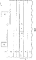
Shown in Figure 1 is a semiconductor device 10, comprise: at silicon-on-insulator (SOI) substrate 12, the gate-dielectric on the upper surface of SOI substrate 12 14 directly, the layer 16 of titanium nitride, the layer 18 of tantalum silicon nitride, the layer 20 of polysilicon, the photoresist part 24 and 26 of anti-reflection coating of the silicon nitride of Silicon-rich (ARC) 22 and formation pattern.SOI substrate 12 has silicon substrate 28, insulator layer 30, N district 34, isolated area 32 and P district 36.Insulating barrier 30 is silica preferably, but can be another kind of insulating material.In addition, Kuai Zhuan silicon substrate can make and be used for replacing the SOI substrate.Floor 16 covers N district 34, rather than P district 36, and directly contacts with gate-dielectric 14.Floor 18 covers the SOI substrate 12 that comprises floor 16 and P district 36.Layer 20 cover layer 18.Layer 22 cover layer 20.The photoresist part 24 that forms pattern covers the part in N district 34, and here the P channel gate stack will be formed.Similarly, the photoresist part 26 that forms pattern covers the part in P district 36, and here the N channel gate stack will be formed.
In this, dry etch is performed, and it does not pass this gate-dielectric 14.The thickness of layer 16 and 18 is 50 dusts preferably, but can hang down to 30 dusts, perhaps can be higher than 50 dusts.Forming preferably 500 dusts of the photoresist part 24 of pattern and 26 width, approximately is ten times of thickness of this metal level 16 and 18, and it will be used to determine the length of transistor gate.The width of isolated area 32 is identical with photoresist part 24 that forms pattern and 26 width approximately.The specific technology that depends on use, these sizes can be littler or bigger.For example, it only is 500 dusts and even 1000 dusts that a photoetching technique difficult problem may limit for the photoresist part 24 of this formation pattern and 26 minimum dimension at manufacture view, but the thickness of layer 16 and 18 can still remain on 50 dusts.ARC layer 22 is 200 dust thickness preferably.
Be the result of dry etch shown in figure 2, it stays gate electrode stack 37 and 39 respectively in N district 34 and P district 36.Except being covered by gate electrode stack 39, gate-dielectric 14 is exposed in the P district 36.Except being covered by gate electrode stack 37, the floor 16 in N district 34 is exposed.The photoresist part 24 and 26 that forms pattern may be corroded. Gate electrode stack 37 and 39 both have ARC 22, the layer 20 and the layer 18 part.
The gate electrode stack 37 of formation Fig. 2 and this dry etch of 39 preferably realize in three etching steps.A step is to be used for this silicon nitride ARC layer 22, and preferably based on reactive ion(ic) etching (RIE) of halogen.It below is the etching of the layer 20 of the polysilicon by RIE in based on the chemically treated process of halogen.Be the etching of layer 18 after this layer 20 etching, it is to carry out by the RIE based on halogen.These are the conventional etchings of layer that are used for these types.The typical etching of titanium nitride is by also based on the RIE of halogen.Along with these difficulty is that this titanium nitride is not selectively sufficiently for this gate-dielectric, in this case, it is silicon oxynitride preferably.Silicon oxynitride has the higher dielectric constant of ratio silicon oxide, and is more durable equally for the RIE etching based on halogen, still, during so etching needs the titanium nitride of thickness, avoids being penetrated as it and is not sufficiently resistive.RIE etching based on halogen changes a little, and is finally tentatively determined based on the etched layer of reality.The etching of these materials is conventional and is determined traditionally.If silica is used as this gate-dielectric, there is identical etch issues, and in fact or even even worse,, be compared to silicon oxynitride or even still less optionally for silica such as those materials that are used to layer 16 and 18 because be used for the typical dry etch that metal comprises material.
The thickness of this titanium nitride wishes to approach for the purpose of handling, but also wishes to have enough thickness for the work function of determining, the transistorized raceway groove that this work function control forms subsequently.This gate-dielectric preferably has the dielectric constant greater than 3.9.The work function that is used for the best of N channel transistor grid and p channel transistor grid is commonly referred to be respectively in the silicon energy band edges, that is, and and 4.1 electronvolt (eV) and 5.2eV.This is real for the silicon of two bulks with for the SOI that partly exhausts.In practice, this may be to be difficult to realize, but preferably, these N channel metal grid should have the work function that is less than or equal to 4.4eV, and these P channel metal grid should have work function greater than 4.6eV for the SOI substrate that partly exhausts or bulk semiconductor substrate, and it is a situation about existing.The layer 16 of titanium nitride has the work function of 4.65ev, and the layer 18 of tantalum silicon nitride has the work function of 4.4eV.For the less work function difference of the SOI substrate that fully exhausts may be satisfactorily.
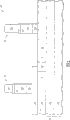
Therefore, replace using conventional RIE etching to come etch layer 16, use wet etching.This wet etching is Pi Lunniya (piranha) cleaning preferably, and it is formed by sulfuric acid with water-soluble hydrogen peroxide.Other wet etchings also can be effective to this.The Pi Lunniya cleaning is useful in particular, because it is available in the assembling facility normally, and therefore, understands better and how to go to be suitable for and control.This Pi Lunniya cleaning is for tantalum silicon nitride and silicon oxynitride, and silica is very selectively.Therefore, during removing the layer 16 that is exposed to this Pi Lunniya cleaning, there are layer 18 and gate-dielectric 14 minimal etchings.If gate-dielectric 14 is silica, this will also be real.
The application result of this Pi Lunniya cleaning is shown in Figure 3.This illustrates finishing of gate electrode stack 37 and to the minimal variation of gate electrode stack 39.The photoresist part 24 and 26 that forms pattern during this Pi Lunniya cleaning is removed.Remove normally scalar property of material with wet cleaning, make laterally and longitudinally etching.Therefore, have the bottom cutting of layer 16, make that the part of layer 16 is removed under the part of this layer 18, the part of this layer 18 is parts of gate electrode stack 37.This bottom cutting is not more than the thickness of etched this layer usually.In this case, the preferred thickness of layer 16 is 50 dusts, and therefore, this bottom cutting on the interface between layer 16 and 18 can approximately be 50 dusts, it approximately is 10% of this grid length, and has still less bottom cutting towards the direction of this gate-dielectric 14.As shown in Figure 3, gate electrode stack 37 and 39 is in order, finishes transistorized formation in a conventional manner.
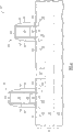
The transistor 38 and 40 that is to use gate electrode stack 37 and 39 to finish shown in Figure 4.ARC layer 22 by from gate electrode stack 37 and 39 both remove, and transistor 38 and 40 can be manufactured in a conventional manner.Transistor is the p channel transistor with source/ drain 42 and 44, sidewall spacer 46, liner 48 and silicide area 50,52 and 54. Silicide area 50 and 52 is formed on source/ drain 42 and 44 respectively, and contacts with 44 with source/drain 42.Similarly, silicide area 54 is formed on layer 20 the part and contacts with these layer 20 parts, and this layer 20 part are the parts of gate electrode stack 37 as shown in Figure 3.Transistor 40 is the N channel transistors with source/ drain regions 56 and 58, sidewall spacer 60, liner 62 and silicide area 64 and 66. Silicide area 64 and 66 is to contact with 58 on source/ drain 56 and 58 and with source/drain 56 respectively.
In above-mentioned specification, the present invention has been described with reference to certain embodiments.But common one skilled in the art will appreciate that does not break away from the scope of the present invention as illustrating in following claim, can carry out various improvement and variation.For example, a selective device structure shown in Figure 1 is own by the covering electric conductor of layer, or the alloy with centigrade concentration of one of this material.In addition, two different layers 16 can be different materials with 18 except appointment herein.In fact these two layers can have identical materials, but have the different ratio of its material, so that obtain the work function difference of expectation.In addition, layer 18 can at first be deposited, and makes that in this middle level, 36 position, P district 16 be on floor 18.This possibility of result is that this N channel transistor gate electrode stack will have two metal levels, replace having the P channel gate stack of two metal levels shown in Fig. 2-4.The example of another alternative is to replace this covering polysilicon layer with the material with lower film resistor (such as tungsten).Therefore, specification and accompanying drawing are to be regarded as illustrative and not restrictive sensation, and all above-mentioned improvement are intended to be included in the scope of the present invention.
Benefit, other advantage have been described in the above and to the solution of problem about certain embodiments.But, benefit, advantage, to the solution of problem, with the solution that may cause any benefit, advantage or appearance, perhaps become any key element of asserting more and be not construed as critical, need, perhaps any or basic characteristics or key element that all authority requires.As using herein, this term " comprises ", " comprising " or its every other variation, be intended to cover non-exclusive inclusion, make processing procedure, method, product or the device comprise a series of key elements not only comprise those key elements, but can comprise and not listing significantly or above-mentioned processing procedure, method, product or install original other key element.
Claims (24)
1. method that is used to form dual metal gate structure comprises:
Semiconductor substrate with first area and second area is provided, and wherein this first area has first conductivity-type and second area has second conductivity-type that is different from this first conductivity-type;
Form one and cover the first area of this Semiconductor substrate and the dielectric layer of second area;
Form first metal that covers this dielectric layer and comprise layer, wherein this first metal comprises the first area that layer covers this Semiconductor substrate;
Form to cover second metal that first metal comprises layer and dielectric layer and comprise layer, wherein second metal comprises layer and directly contacts with the part of this dielectric layer of the second area of covering Semiconductor substrate;
Form and cover the pattern mask layer that second metal comprises layer, to determine that first grid is stacked and second grid is stacked;
Use this pattern mask layer dry ecthing second metal to comprise layer, stacked on the first area, to form this first grid, and it is stacked to form this second grid on second area, wherein, except by the stacked covering of first grid, described first metal comprises layer and is exposed; With
This first metal of wet etching comprises layer, and the bottom cuts described first metal and comprise layer, and a part that makes described first metal comprise layer is comprised from stacked described second metal of described first grid under the layer removes.
According to the process of claim 1 wherein this first and second metal comprise the layer a work function with at least 4.6 electronvolt (eV), and this first and second metal comprise the layer another have the work function of 4.4eV at the most.
According to the process of claim 1 wherein this first and second metal comprise the layer each have the thickness of at least 30 dusts.
4. according to the process of claim 1 wherein that this second metal comprises layer and comprises alloy.
According to the process of claim 1 wherein this first and second metal comprise the layer each comprise alloy.
According to the process of claim 1 wherein this first metal of wet etching comprise the layer comprise run through this first metal comprise the layer whole thickness wet etching.
7. according to the process of claim 1 wherein that wet etching is to use the Pi Lunniya cleaning to carry out.
8. according to the process of claim 1 wherein that this dielectric layer comprises the dielectric of (K) at least 3.9 that have dielectric constant.
9. according to the process of claim 1 wherein that this first conductivity-type is N type or P type one, and second conductivity-type is N type or P type another.
10. method that is used to form dual metal gate structure, it comprises:
Semiconductor substrate with first area and second area is provided, and wherein this first area has first conductivity-type, and second area has second conductivity-type that is different from this first conductivity-type;
Form the first area of this Semiconductor substrate of covering and the dielectric layer of second area;
Form first metal that covers this dielectric layer and comprise layer, wherein this first metal comprises the first area that layer covers this Semiconductor substrate;
Form to cover second metal that first metal comprises layer and dielectric layer and comprise layer, wherein second metal comprises layer and directly contacts with the part of this dielectric layer of the second area of covering Semiconductor substrate;
Form and cover the pattern mask layer that second metal comprises layer, to determine that first grid is stacked and second grid is stacked;
Use this pattern mask layer dry ecthing second metal to comprise layer, to form the stacked gate electrode of this first grid; And
Use this pattern mask layer wet etching first metal to comprise layer, to form the stacked gate electrode of this second grid;
Wherein this first and second metal comprise the layer one comprise titanium nitride, and this first and second metal comprise the layer another comprise tantalum silicon nitride.
11. a method that is used to form dual metal gate structure, it comprises:
Semiconductor substrate with first area and second area is provided, and wherein this first area has first conductivity-type, and second area has second conductivity-type that is different from this first conductivity-type;
Form the first area of this Semiconductor substrate of covering and the dielectric layer of second area;
Form first metal that covers this dielectric layer and comprise layer, wherein this first metal comprises the first area that layer covers this Semiconductor substrate;
Form to cover second metal that first metal comprises layer and dielectric layer and comprise layer, wherein this second metal comprises layer and directly contacts with the part of this dielectric layer of the second area of covering Semiconductor substrate;
Form and cover the pattern mask layer that second metal comprises layer, to determine that first grid is stacked and second grid is stacked;
Use this pattern mask layer dry ecthing second metal to comprise layer, to form the stacked gate electrode of this first grid; And
Use this pattern mask layer wet etching first metal to comprise layer, forming the stacked gate electrode of this second grid,
Wherein, before form covering the pattern mask layer that second metal comprises layer, form and cover the silicon that second metal comprises layer and comprise layer, wherein this pattern mask layer covers this silicon and comprises layer, uses this this silicon of pattern mask layer dry ecthing to comprise layer.
12. the method according to claim 11 further comprises:
Form one and cover the antireflecting coating that this silicon comprises layer, wherein this pattern mask layer covers this antireflecting coating; With
Use this this antireflecting coating of pattern mask layer dry ecthing.
13. the method according to claim 12 further comprises:
In first and second zones of this Semiconductor substrate of adjacent this first and second gate electrode stack, form doped region and adjacent this first and second gate electrode stack forms sidewall spacer, to form the first transistor and transistor seconds.
14. a method that is used to form dual metal gate structure comprises:
Semiconductor substrate with first area and second area is provided, and wherein one of this first and second zone is the P district, and another of this first and second zone is the N district;
Form one and cover the first area of this Semiconductor substrate and the gate dielectric of second area;
Form first metal that covers this dielectric layer and comprise layer, wherein this first metal comprises the first area that layer covers this Semiconductor substrate;
Second metal that this first metal of formation covering comprises layer and this dielectric layer comprises layer, wherein this second metal comprises layer and directly contacts with the part of this dielectric layer of the second area of this Semiconductor substrate of covering, and wherein this first and second containing metal comprise the layer one comprise titanium nitride, and this first and second metal comprise the layer another comprise tantalum silicon nitride;
Form and cover the pattern mask layer that this second metal comprises layer, to determine that first grid is stacked and second grid is stacked;
Use this this second metal of pattern mask layer dry ecthing to comprise layer, to form the stacked gate electrode of this first grid; With
Use this this first metal of pattern mask layer wet etching to comprise at least a portion of layer, to form the stacked gate electrode of second grid.
15. according to the method for claim 14, wherein this first and second metal comprise the layer each have the thickness of at least 30 dusts.
16. according to the method for claim 14, wherein this first area is the N district, and second area is the P district.
17. a method that is used to form dual metal gate structure comprises:
Semiconductor substrate with first area and second area is provided, and wherein this first area has first conductivity-type and second area has second conductivity-type that is different from this first conductivity-type;
Form the dielectric layer that covers this Semiconductor substrate;
It is stacked to form the first grid that covers this first area, this first grid is stacked to have and covers and first metal that physics contacts this dielectric layer comprises gate electrode, wherein form this first grid stacked be included in dry ecthing cover first metal comprise the layer second metal comprise after the layer, wet etching first metal comprises layer, comprises gate electrode to form this first metal; With
It is stacked to form the second grid that covers this second area, this second grid is stacked to have and covers and second metal that physics contacts this dielectric layer comprises gate electrode, wherein form stacked dry ecthing second metal that comprises of this second grid and comprise layer, comprise gate electrode to form this second metal, wherein this first metal comprises gate electrode and has first work function and second metal and comprise gate electrode and have second work function that is different from this first work function.
18. according to the method for claim 17, wherein one of this first and second work function is 4.6eV at least, and another of this first and second work function is 4.4eV at the most.
19. according to the method for claim 17, wherein this first and second metal comprise gate electrode each have the thickness of at least 30 dusts.
20. according to the method for claim 17, wherein this first and second metal comprise gate electrode at least one comprise alloy.
21. a method that is used to form dual metal gate structure, it comprises:
Semiconductor substrate with first area and second area is provided, and wherein the first area has first conductivity-type, and second area has second conductivity-type that is different from first conductivity-type;
Form the dielectric layer that covers Semiconductor substrate;
It is stacked to form the first grid that covers the first area, this first grid is stacked to have and covers and first metal of physics contact dielectric layer comprises gate electrode, forms wherein that first grid is stacked to comprise that wet etching first metal comprises layer and comprises gate electrode to form first metal; And
It is stacked to form the second grid that covers second area, stacked second metal with covering and physics contact dielectric layer of this second grid comprises gate electrode, wherein form this second grid stacked comprise dry ecthing second metal comprise the layer comprise gate electrode to form second metal, and wherein said first metal comprises gate electrode and has first work function, and second metal comprises gate electrode and has second work function that is different from first work function.
Form wherein that this first grid is stacked to comprise that further form covering first silicon that this first metal comprises gate electrode comprises part, cover the first anti-reflective coating part that this first silicon comprises part with forming, and wherein, form that this second grid is stacked to comprise that further form covering second silicon that this second metal comprises gate electrode comprises part and form and cover the second anti-reflective coating part that this second silicon comprises part.
22. a method that is used to form bimetal structure, it comprises:
Semiconductor substrate with first area and second area is provided, and wherein the first area has first conductivity-type, and second area has second conductivity-type that is different from first conductivity-type;
Form the dielectric layer that covers Semiconductor substrate;
It is stacked to form the first grid that covers the first area, this first grid is stacked to have and covers and first metal of physics contact dielectric layer comprises gate electrode, forms wherein that first grid is stacked to comprise that wet etching first metal comprises layer and comprises gate electrode to form first metal; And
It is stacked to form the second grid that covers second area, stacked second metal with covering and physics contact dielectric layer of this second grid comprises gate electrode, wherein form this second grid stacked comprise dry ecthing second metal comprise the layer comprise gate electrode to form second metal, and wherein said first metal comprises gate electrode and has first work function, and second metal comprises gate electrode and has second work function that is different from first work function.
Wherein this first and second metal comprises of gate electrode and comprises titanium nitride, and this first and second metal comprise gate electrode another comprise tantalum silicon nitride.
23. according to the method for claim 22, wherein this first conductivity-type is N type or P type one, and second conductivity-type is N type or P type another.
24. according to the method for claim 23, wherein this first conductivity-type is that N type and this second conductivity-type are the P types.
Applications Claiming Priority (2)
| Application Number | Priority Date | Filing Date | Title |
|---|---|---|---|
| US10/410,043 | 2003-04-09 | ||
| US10/410,043 US6790719B1 (en) | 2003-04-09 | 2003-04-09 | Process for forming dual metal gate structures |
Publications (2)
| Publication Number | Publication Date |
|---|---|
| CN1771590A CN1771590A (en) | 2006-05-10 |
| CN100487880C true CN100487880C (en) | 2009-05-13 |
Family
ID=32927360
Family Applications (1)
| Application Number | Title | Priority Date | Filing Date |
|---|---|---|---|
| CNB2004800094963A Expired - Fee Related CN100487880C (en) | 2003-04-09 | 2004-04-08 | Process for forming dual metal gate structures |
Country Status (6)
| Country | Link |
|---|---|
| US (1) | US6790719B1 (en) |
| JP (1) | JP4653735B2 (en) |
| KR (1) | KR101159339B1 (en) |
| CN (1) | CN100487880C (en) |
| TW (1) | TWI342044B (en) |
| WO (1) | WO2004093182A1 (en) |
Families Citing this family (48)
| Publication number | Priority date | Publication date | Assignee | Title |
|---|---|---|---|---|
| JP3790237B2 (en) * | 2003-08-26 | 2006-06-28 | 株式会社東芝 | Manufacturing method of semiconductor device |
| US7125775B1 (en) * | 2004-03-18 | 2006-10-24 | Integrated Device Technology, Inc. | Method for forming hybrid device gates |
| US7030001B2 (en) * | 2004-04-19 | 2006-04-18 | Freescale Semiconductor, Inc. | Method for forming a gate electrode having a metal |
| DE102004026232B4 (en) * | 2004-05-28 | 2006-05-04 | Infineon Technologies Ag | A method of forming a semiconductor integrated circuit device |
| KR100602122B1 (en) * | 2004-12-03 | 2006-07-19 | 동부일렉트로닉스 주식회사 | Method of manufacturing semiconductor device |
| US7109079B2 (en) * | 2005-01-26 | 2006-09-19 | Freescale Semiconductor, Inc. | Metal gate transistor CMOS process and method for making |
| JP4764030B2 (en) | 2005-03-03 | 2011-08-31 | 株式会社東芝 | Semiconductor device and manufacturing method thereof |
| JP4626411B2 (en) * | 2005-06-13 | 2011-02-09 | ソニー株式会社 | Semiconductor device and manufacturing method of semiconductor device |
| US20070048920A1 (en) * | 2005-08-25 | 2007-03-01 | Sematech | Methods for dual metal gate CMOS integration |
| US7332433B2 (en) * | 2005-09-22 | 2008-02-19 | Sematech Inc. | Methods of modulating the work functions of film layers |
| JP4723975B2 (en) | 2005-10-25 | 2011-07-13 | 株式会社東芝 | Semiconductor device and manufacturing method thereof |
| JP2007123548A (en) * | 2005-10-28 | 2007-05-17 | Renesas Technology Corp | Manufacturing method for semiconductor device |
| US20070178634A1 (en) * | 2006-01-31 | 2007-08-02 | Hyung Suk Jung | Cmos semiconductor devices having dual work function metal gate stacks |
| KR100827435B1 (en) * | 2006-01-31 | 2008-05-06 | 삼성전자주식회사 | Method of fabricating gate with oxygen free ashing process in semiconductor device |
| JP4929867B2 (en) * | 2006-06-19 | 2012-05-09 | 富士通セミコンダクター株式会社 | Manufacturing method of semiconductor device |
| KR100835430B1 (en) * | 2007-05-21 | 2008-06-04 | 주식회사 동부하이텍 | Method for forming dual gate electrode of semiconductor device |
| US7696036B2 (en) * | 2007-06-14 | 2010-04-13 | International Business Machines Corporation | CMOS transistors with differential oxygen content high-k dielectrics |
| US7666730B2 (en) * | 2007-06-29 | 2010-02-23 | Freescale Semiconductor, Inc. | Method for forming a dual metal gate structure |
| KR100903383B1 (en) * | 2007-07-31 | 2009-06-23 | 주식회사 하이닉스반도체 | Transistor hvaing gate elcetode with tuning of work function and memory device with the same |
| JP2009044051A (en) * | 2007-08-10 | 2009-02-26 | Panasonic Corp | Semiconductor device and its manufacturing method |
| US20090206416A1 (en) * | 2008-02-19 | 2009-08-20 | International Business Machines Corporation | Dual metal gate structures and methods |
| US7691701B1 (en) * | 2009-01-05 | 2010-04-06 | International Business Machines Corporation | Method of forming gate stack and structure thereof |
| DE102009039418B4 (en) * | 2009-08-31 | 2013-08-22 | GLOBALFOUNDRIES Dresden Module One Ltd. Liability Company & Co. KG | Adjustment of work function in high-k gate stacks containing gate dielectrics of different thickness |
| US8435878B2 (en) * | 2010-04-06 | 2013-05-07 | International Business Machines Corporation | Field effect transistor device and fabrication |
| US8211775B1 (en) | 2011-03-09 | 2012-07-03 | United Microelectronics Corp. | Method of making transistor having metal gate |
| US8519487B2 (en) | 2011-03-21 | 2013-08-27 | United Microelectronics Corp. | Semiconductor device |
| US9384962B2 (en) | 2011-04-07 | 2016-07-05 | United Microelectronics Corp. | Oxygen treatment of replacement work-function metals in CMOS transistor gates |
| US8530980B2 (en) | 2011-04-27 | 2013-09-10 | United Microelectronics Corp. | Gate stack structure with etch stop layer and manufacturing process thereof |
| US8673758B2 (en) | 2011-06-16 | 2014-03-18 | United Microelectronics Corp. | Structure of metal gate and fabrication method thereof |
| US9490342B2 (en) | 2011-06-16 | 2016-11-08 | United Microelectronics Corp. | Method for fabricating semiconductor device |
| US8536038B2 (en) | 2011-06-21 | 2013-09-17 | United Microelectronics Corp. | Manufacturing method for metal gate using ion implantation |
| US8486790B2 (en) | 2011-07-18 | 2013-07-16 | United Microelectronics Corp. | Manufacturing method for metal gate |
| US8551876B2 (en) | 2011-08-18 | 2013-10-08 | United Microelectronics Corp. | Manufacturing method for semiconductor device having metal gate |
| US8872286B2 (en) | 2011-08-22 | 2014-10-28 | United Microelectronics Corp. | Metal gate structure and fabrication method thereof |
| US8691681B2 (en) | 2012-01-04 | 2014-04-08 | United Microelectronics Corp. | Semiconductor device having a metal gate and fabricating method thereof |
| US8860181B2 (en) | 2012-03-07 | 2014-10-14 | United Microelectronics Corp. | Thin film resistor structure |
| US9105623B2 (en) | 2012-05-25 | 2015-08-11 | United Microelectronics Corp. | Semiconductor device having metal gate and manufacturing method thereof |
| US8975666B2 (en) | 2012-08-22 | 2015-03-10 | United Microelectronics Corp. | MOS transistor and process thereof |
| US9054172B2 (en) | 2012-12-05 | 2015-06-09 | United Microelectrnics Corp. | Semiconductor structure having contact plug and method of making the same |
| US8735269B1 (en) | 2013-01-15 | 2014-05-27 | United Microelectronics Corp. | Method for forming semiconductor structure having TiN layer |
| US9653300B2 (en) | 2013-04-16 | 2017-05-16 | United Microelectronics Corp. | Structure of metal gate structure and manufacturing method of the same |
| US9159798B2 (en) | 2013-05-03 | 2015-10-13 | United Microelectronics Corp. | Replacement gate process and device manufactured using the same |
| US9196542B2 (en) | 2013-05-22 | 2015-11-24 | United Microelectronics Corp. | Method for manufacturing semiconductor devices |
| US8921947B1 (en) | 2013-06-10 | 2014-12-30 | United Microelectronics Corp. | Multi-metal gate semiconductor device having triple diameter metal opening |
| US9105720B2 (en) | 2013-09-11 | 2015-08-11 | United Microelectronics Corp. | Semiconductor device having metal gate and manufacturing method thereof |
| US20150069534A1 (en) | 2013-09-11 | 2015-03-12 | United Microelectronics Corp. | Semiconductor device and method for fabricating the same |
| US9196546B2 (en) | 2013-09-13 | 2015-11-24 | United Microelectronics Corp. | Metal gate transistor |
| US9231071B2 (en) | 2014-02-24 | 2016-01-05 | United Microelectronics Corp. | Semiconductor structure and manufacturing method of the same |
Family Cites Families (8)
| Publication number | Priority date | Publication date | Assignee | Title |
|---|---|---|---|---|
| US6004869A (en) | 1997-04-25 | 1999-12-21 | Micron Technology, Inc. | Method for making a low resistivity electrode having a near noble metal |
| US6171959B1 (en) * | 1998-01-20 | 2001-01-09 | Motorola, Inc. | Method for making a semiconductor device |
| US6166417A (en) * | 1998-06-30 | 2000-12-26 | Intel Corporation | Complementary metal gates and a process for implementation |
| JP2002083812A (en) * | 1999-06-29 | 2002-03-22 | Semiconductor Energy Lab Co Ltd | Wiring material and semiconductor device with the wiring material and its manufacturing device |
| US6171910B1 (en) * | 1999-07-21 | 2001-01-09 | Motorola Inc. | Method for forming a semiconductor device |
| US6214681B1 (en) * | 2000-01-26 | 2001-04-10 | Advanced Micro Devices, Inc. | Process for forming polysilicon/germanium thin films without germanium outgassing |
| US6444512B1 (en) | 2000-06-12 | 2002-09-03 | Motorola, Inc. | Dual metal gate transistors for CMOS process |
| KR100399356B1 (en) * | 2001-04-11 | 2003-09-26 | 삼성전자주식회사 | Method of forming cmos type semiconductor device having dual gate |
-
2003
- 2003-04-09 US US10/410,043 patent/US6790719B1/en not_active Expired - Lifetime
-
2004
- 2004-04-08 CN CNB2004800094963A patent/CN100487880C/en not_active Expired - Fee Related
- 2004-04-08 JP JP2006509809A patent/JP4653735B2/en not_active Expired - Fee Related
- 2004-04-08 WO PCT/US2004/010814 patent/WO2004093182A1/en active Application Filing
- 2004-04-08 KR KR1020057019065A patent/KR101159339B1/en not_active IP Right Cessation
- 2004-04-09 TW TW093110018A patent/TWI342044B/en not_active IP Right Cessation
Also Published As
| Publication number | Publication date |
|---|---|
| JP2006523037A (en) | 2006-10-05 |
| CN1771590A (en) | 2006-05-10 |
| JP4653735B2 (en) | 2011-03-16 |
| KR101159339B1 (en) | 2012-06-25 |
| WO2004093182A1 (en) | 2004-10-28 |
| US6790719B1 (en) | 2004-09-14 |
| KR20050120785A (en) | 2005-12-23 |
| TW200507099A (en) | 2005-02-16 |
| TWI342044B (en) | 2011-05-11 |
Similar Documents
| Publication | Publication Date | Title |
|---|---|---|
| CN100487880C (en) | Process for forming dual metal gate structures | |
| US6500756B1 (en) | Method of forming sub-lithographic spaces between polysilicon lines | |
| US20050026345A1 (en) | Process for forming dual metal gate structures | |
| KR100546378B1 (en) | Method of manufacturing transistor having recessed channel | |
| US20040115896A1 (en) | MOS transistor having a T-shaped gate electrode and method for fabricating the same | |
| US6664173B2 (en) | Hardmask gate patterning technique for all transistors using spacer gate approach for critical dimension control | |
| KR100816733B1 (en) | Method for fabricating recess gate in semiconductor device | |
| US20130059441A1 (en) | Method for fabricating a semiconductor structure | |
| US5989987A (en) | Method of forming a self-aligned contact in semiconductor fabrications | |
| KR100469913B1 (en) | Manufacturing method for semiconductor device | |
| US6849530B2 (en) | Method for semiconductor gate line dimension reduction | |
| US6797552B1 (en) | Method for defect reduction and enhanced control over critical dimensions and profiles in semiconductor devices | |
| US6413846B1 (en) | Contact each methodology and integration scheme | |
| JPH11330262A (en) | Manufacture of semiconductor device | |
| US7491644B2 (en) | Manufacturing process for a transistor made of thin layers | |
| US6812077B1 (en) | Method for patterning narrow gate lines | |
| KR100214534B1 (en) | Method of forming a device isolation structure of semiconductor device | |
| KR20050070320A (en) | Method for forming gate electrode in semiconductor device | |
| US7268066B2 (en) | Method for semiconductor gate line dimension reduction | |
| KR101073127B1 (en) | Method for manufacturing gate-line in semiconductor device | |
| JP2944902B2 (en) | Method for manufacturing field effect transistor | |
| US5945355A (en) | Integrated circuit fabrication | |
| KR101057698B1 (en) | Method of forming silicide film of semiconductor device | |
| KR100261867B1 (en) | Device and method for forming gate electrode of mos transistor | |
| TWI515800B (en) | Semiconductor device having metal gate and manufacturing method thereof |
Legal Events
| Date | Code | Title | Description |
|---|---|---|---|
| C06 | Publication | ||
| PB01 | Publication | ||
| C10 | Entry into substantive examination | ||
| SE01 | Entry into force of request for substantive examination | ||
| C14 | Grant of patent or utility model | ||
| GR01 | Patent grant | ||
| CP01 | Change in the name or title of a patent holder | ||
| CP01 | Change in the name or title of a patent holder |
Address after: Texas in the United States Patentee after: NXP America Co Ltd Address before: Texas in the United States Patentee before: Fisical Semiconductor Inc. |
|
| CF01 | Termination of patent right due to non-payment of annual fee | ||
| CF01 | Termination of patent right due to non-payment of annual fee |
Granted publication date: 20090513 Termination date: 20190408 |